國 立 交 通 大 學
電子工程學系 電子研究所碩士班
碩 士 論 文
矽基板上新穎結構的非揮發性記憶體與互補式金氧
半場效電晶體的研究
Novel Structures of Nonvolatile Memory and CMOS on
Bulk Silicon
研 究 生:陳宣凱
指導教授:簡昭欣 教授
矽基板上新穎結構的非揮發性記憶體與互補式金氧
半場效電晶體的研究
Novel Structures of Nonvolatile Memory and CMOS on
Bulk Silicon
研 究 生:陳宣凱 Student:Hsuan-Kai Chen
指導教授:簡昭欣 Advisor:Chao-Hsin Chien
國 立 交 通 大 學
電子工程學系 電子研究所碩士班
碩 士 論 文
A Thesis
Submitted to Department of Electronics Engineering & Institute of Electronics
College of Electrical Engineering and Computer Engineering
National Chiao Tung University
In Partial Fulfillment of the Requirements
For the Degree of
Master
In
Electronics Engineering
September 2009
Hsinchu, Taiwan
中華民國九十八年九月
i
矽基板上新穎結構的非揮發性記憶體與互補式金氧
半場效電晶體的研究
研究生:陳宣凱
指導教授:簡昭欣 教授
國立交通大學
電子工程學系
電子研究所碩士班
摘要
此論文在傳統矽基板上製做不同的新型結構元件,包含了非揮發記憶體與基板分 割的場效電晶體。 首先,我們使用不同的結構來製做非揮發記憶體。傳統上,非揮發記憶體的閘極 絕緣體堆疊結構為氧化矽-氮化矽-氧化矽,與單純一層氧化矽製做的邏輯元件有很大 的差距。在我們的結構中,閘極電極下方與邏輯元件一樣只有單純一層氧化矽,而電荷 捕捉層是由矽酸鉿退火型成的奈米微晶粒構成,此捕捉層的位置是在氮化矽的隔離層下 方。而此隔離層下方並沒有源極/汲極的任何離子佈植。此結構的記憶體提供了寫入與 抹除的特性,我們也會討論此元件的資料持久性與抗干擾的能力。這種結構的非揮發記ii 憶體對於未來希望在同一晶片上製做非揮發記憶體與邏輯元件的技術是非常有潛力 的。若能把非揮發記憶體與邏輯元件製做在同一晶片上,可以有效提升系統的速度。 接著,我們在矽基板上製做了 n 型場效電晶體。這種三通道閘極的結構通常使用 在絕緣體上矽基板上。我們發現蝕刻小部分的淺溝槽隔離氧化矽可以有效的改善元見的 次臨界擺幅。並且可以降低臨界電壓。在本體效應的量測中,我們發現在比較窄的閘極 寬度或是蝕刻比較深的淺溝槽隔離氧化矽之下,本體的電壓對通道的影響會受到側壁的 空乏區的影響而阻隔。 最後,我們製做了同樣結構的 p 型場效電晶體。這些 p 型場效電晶體,與n型場 效電晶體有類似的電性趨勢,在某些部份改善了電晶體的電性。因此在矽基板上製做的 三通道元件可以改善CMOS元件的特性。
iii
Novel Structures of Nonvolatile Memory and CMOS
on Bulk Silicon
Student:Hsuan-Kai Chen Advisor:Dr. Chao-Hsin Chien
Department of Electronics Engineering & Institute of Electronics
National Chiao Tung University
Abstract
In this thesis, we fabricated non-typical devices on the silicon bulk for nonvolatile memory and segment-MOSFET.
First, we will present a novel nonvolatile flash memory process with only silicon oxide under the gate electrode instead of the oxide-nitride-oxide structure. The storage layer, which is fabricated by hafnium silicate (HfSiOx) as the trapping material, is deposited under the nitride spacer. No LDD dopant is implanted under the spacer stack, so there is no overlapped region between source/drain and gate electrode. These nonvolatile memories exhibit programming characteristics and erase characteristics. Also the retention and disturbance characteristics of these devices will be discussed. Since the fabrication process of the nonvolatile memory is similar to the logic device, the structure will become attractive if it is possible to fabricate the nonvolatile memory embedded with the logic device.
iv
Next, we fabricated the segment n-MOSFET on the silicon bulk. The FINFET structure is usually fabricated on the SOI wafer. We found that the recess of shallow-trench-isolation oxide enhances the subthreshold swing characteristics and decreases the threshold voltage, and the body voltage is blocked during the body effect measuring.
Finally, the segment p-MOSFET was fabricated with the same process as the segment n-MOSFET. The trend of p-MOSFET is similar to n-MOSFET, so the FIN structure also improves some performance on silicon bulk for CMOS process.
v
誌謝
能在人生中走到這個階段,首先要先感謝我的父母對我的栽培跟容忍,讓我有機 會可以無後顧之憂的念書到這邊,並且不必擔心太多事情。 而在論文完成的過程,最需要感謝的就是指導老師簡昭欣博士,老師提供了充分 的研究資源讓我們可以盡情發揮,也裝潢了很舒服的研究室讓我們使用,而老師對研究 嚴謹而對人溫和的態度也讓我們在努力提升自己的能力的同時,勇於跟老師討論課業上 與課業外的各種問題。 感謝振華、豪育、明瑞、志彥、宗元、兆欽、世璋、豐綺、峻丞、家豪、治國、 競之、宜憲、妍心和韶華等學長姐在實驗上最大的協助與不厭其煩的指導,讓我有了所 有的資源來完成我的研究。 還有實驗室同學欣哲、効諭、宇彥、登偉、敬倫、弘森、猛飛在共同研究時的討 論與給我的幫助,還有在課業以外的生活,讓我的研究生涯更加豐富! 實驗室的柏錡、政庭、宗佑、文朋、耀陞、國永、宗霖、宏基、禎晏等學弟的大 力幫忙,沒有你們的話,我的論文不可能順利完成! 除了我們實驗室之外,我也請教了很多其他實驗室同學或是學長姐學弟妹,也受 了很多幫忙,因為我麻煩過的人實在太多,在這邊無法一一列出,但是實在非常感謝你 們。 感謝交大奈米中心與國家奈米元件實驗室的所有研究員、工程師、操作員與行政 人員在實驗上的協助,讓我能在最好的環境下做半導體製程的實驗並且學習到很多經 驗。 也要感謝從大學時代開始,交大電子系所與外系所有指導過我的老師,在各位教 授的課堂上一點一滴的學習,讓我的能力也一點一點的進步。 謝謝交大電子系所、幼幼社、系羽、圍棋社、還有至善協會的夥伴們,讓我在交 大的期間除了課業上,在課業外也獲得了很大的舒壓與成就感,並且交到了許多好朋vi 友,也要感謝我在幼幼社與至善協會帶過的小朋友們,願你們的成長過程都能夠充實而 且快樂! 最後要感謝我所有的家人跟朋友在我一生中給我的支持與鼓勵,還有希望去年過 世的外婆在天之靈能夠一切安好。 在論文最後完成的過程中,莫拉克颱風在台灣造成了非常嚴重的八八水災,在電 視上看到受災的慘狀為之鼻酸,卻沒有能力付出太多時間與金錢去幫忙,所幸看到全台 灣人的凝聚力不下十年前的大地震,相信台灣的未來一定會更好。
vii
Contents
Abstract (Chinese) ---
iAbstract (English) ---
iiiAcknowledge ---
vContents ---
viiTable Captions ---
xiFigure Captions ---
xiiChapter 1 Introduction ---
11.1 Background ---1
1.1.1 Background of Nonvolatile Memory --- 1
1.1.2 Background of Segmented MOSFET --- 3
1.2 Motivation --- 3
1.2.1 Motivation of Nonvolatile Memory --- 3
1.2.2 Motivation of Segmented MOSFET --- 4
1.3 Thesis Organization --- 4
Chapter 2 Characteristics of Nonoverlapped Implantation
Nonvolatile Memory ---
52.1 Introduction --- 5
2.2 Device Fabrication --- 5
viii
2.3.1 Measurement of Threshold Voltage --- 6
2.3.2 Drain Current vs Gate Voltage --- 7
2.3.2 Programming Characteristics --- 7 2.3.2.1 Programming Mechanism --- 7 2.3.2.2 Programming Properties --- 7 2.3.3 Erasing Characteristics --- 8 2.3.3.1 Erasing Mechanism --- 8 2.3.3.2 Erasing Properties --- 8 2.3.4 Retention Characteristics --- 9 2.3.4.1 Retention mechanism --- 9 2.3.4.2 Retention Properties --- 9 2.3.5 Disturbance Characteristics --- 10 2.3.5.1 Disturbance Mechanism --- 10 2.3.5.2 Disturbance Properties --- 10 2.4 Summary --- 11
Chapter 3 Characteristics of Segmented n-MOSFET ---
323.1 Introduction --- 32
3.2 Device Fabrication --- 32
3.3 Results and Discussion --- 33
3.3.1 Device Structure of 3-point SegFETs --- 33
3.3.2 Drain Current vs. Gate Voltage Curve --- 33
3.3.3 FIN Number and Electrical Properties --- 33
3.3.4 Drain Current vs. Gate Length --- 33
ix
3.3.6 Device structure of 4-point Devices --- 35
3.3.7 Threshold Voltage vs. Gate length on 4-point Devices --- 35
3.3.8 Threshold Voltage vs. Gate width on 4-point Devices --- 35
3.3.9 Body Effect on 4-point Devices --- 35
3.3.10 Kink Effect --- 36
3.4 Summary --- 36
Chapter 4 Characteristics of Segmented p-MOSFET ---
534.1 Introduction --- 53
4.2 Device Fabrication --- 53
4.3 Results and Discussion --- 53
4.3.1 Device Structure of 3-point SegFETs --- 53
4.3.2 Drain Current vs. Gate Voltage Curve --- 54
4.3.3 FIN Number and Electrical Properties --- 54
4.3.4 Drain Current vs. Gate Length --- 54
4.3.5 Threshold Voltage and Subthreshold Swing vs. Gate length --- 55
4.3.6 Device structure of 4-point Devices --- 55
4.3.7 Threshold Voltage vs. Gate length on 4-point Devices --- 56
4.3.8 Threshold Voltage vs. Gate width on 4-point Devices --- 56
4.3.9 Body Effect on 4-point Devices --- 56
4.4 Summary --- 57
Chapter 5 Conclusion and Future Work ---
675.1 Conclusions --- 67
x
5.2.1 Future Work of Nonoverlapped Implantation Nonvolatile Memory --- 68
5.2.2 Future Work of Segmented MOSFET --- 68
Reference ---
69xi
Table Captions
Chapter 2
xii
Figure Captions
Chapter 2
Fig. 2-1 structures of nonoverlapped implantation nonvolatile memory --- 13
Fig. 2-2 fabrication process of nonoverlapped implantation nonvolatile memory --- 14
Fig. 2-3 TEM picture of nonoverlapped implantation nonvolatile memory --- 15
Fig. 2-4 structure of logic device with similar fabrication process of nonoverlapped implantation nonvolatile memory --- 16
Fig. 2-5 ID-VG curves of two states with(a) dry oxide (b) TEOS oxide as the tunneling/blocking oxide --- 17
Fig. 2-6 channel-hot-electron injection programming mechanism --- 18
Fig. 2-7 programming characteristics with different tunneling/blocking oxide --- 19
Fig. 2-8 programming characteristics with different gate bias --- 20
Fig. 2-9 programming characteristics with different drain bias --- 21
Fig. 2-10 band-to-band-hot-hole injection erasing mechanism --- 22
Fig. 2-11 erasing characteristics with different tunneling/blocking oxide --- 23
Fig. 2-12 erasing characteristics with different gate bias --- 24
Fig. 2-13 erasing characteristics with different drain bias --- 25
Fig. 2-14 retention characteristics with (a)dry oxide (b)TEOS oxide as the tunneling/blocking oxide --- 26
Fig. 2-15 electrons trapped in the spacer (a)before (b)after the charge migration --- 27
Fig. 2-16 NOR array circuit for nonvolatile memory --- 28
Fig. 2-17 read disturbance characteristics with (a)dry oxide (b)TEOS oxide as tunneling/blocking oxide --- 29 Fig. 2-18 gate disturbance characteristics with (a)dry oxide (b)TEOS oxide as
xiii
tunneling/blocking oxide --- 30
Fig. 2-19 drain disturbance characteristics with (a)dry oxide (b)TEOS oxide as tunneling/blocking oxide --- 31
Chapter 3
Fig. 3-1 fabrication process of Segmented MOSFET --- 37Fig. 3-2 TEM pictures of Segmented MOSFET --- 38
Fig. 3-3 scheme of top view of Segmented MOSFET --- 39
Fig. 3-4 ID-VG curves for(a) different STI recess thickness (b) different gate length ---- 40
Fig. 3-5 on current vs. FIN number for (a)10nm (b)15nm (c)30nm STI oxide recess ---- 41
Fig. 3-6 threshold voltage vs. FIN number for (a)10nm (b)15nm (c)30nm STI oxide recess --- 42
Fig. 3-7 on current vs. gate length which on current is normalized by (a) top gate width (b) total gate width --- 43
Fig. 3-8 threshold voltage vs. gate length --- -44
Fig. 3-9 subthreshold swing vs. gate length --- 45
Fig. 3-10 scheme of sidewall depletion region with different STI recess thickness --- 46
Fig. 3-11 scheme of top view of 4-point FINFET --- 47
Fig. 3-12 threshold voltage vs. gate length on 4-point FINFET --- 48
Fig. 3-13 threshold voltage vs. gate width on 4-point FINFET --- 49
Fig. 3-14 scheme of sidewall depletion region with different gate width --- 50
Fig. 3-15 body effect between different gate width --- 51
Fig. 3-16 ID-VD curves for (a) 10nm (b) 15nm (c) 30nm STI oxide recess --- 52
xiv
Fig. 4-1 ID-VG curves for(a) different STI recess thickness (b) different gate length ---- 58
Fig. 4-2 on current vs. FIN number for (a)10nm (b)15nm (c)30nm STI oxide recess --- 59
Fig. 4-3 threshold voltage vs. FIN number for (a)10nm (b)15nm (c)30nm STI oxide recess --- 60
Fig. 4-4 on current vs. gate length which on current is normalized by (a) top gate width (b) total gate width --- 61
Fig. 4-5 threshold voltage vs. gate length --- 62
Fig. 4-6 subthreshold swing vs. gate length --- 63
Fig. 4-7 threshold voltage vs. gate length on 4-point FINFET --- 64
Fig. 4-8 threshold voltage vs. gate width on 4-point FINFET --- 65
1
Chapter 1
Introduction
1.1 Background
1.1.1 Background of Nonvolatile Memory
Nonvolatile memory (NVM) with metal-oxide-semiconductor(MOS) technologies has developed rapidly for mobile electronics products. For example, cell phones, digital cameras, USB flash device, and mp3 walkman all need large storage capacity of NVM.
Volatile memory will lose stored information once the power supply is switched off. The other kind of memory is nonvolatile memory, which does not lose stored data when the power supply is turned off.
D. Kahng and S. M. Sze invented the first floating-gate nonvolatile semiconductor
memory at Bell Labs[1]. Recently, flash memory, which has a byte-selectable programming and sector erasing operation is the most widespread nonvolatile memory. Nevertheless, the floating-gate nonvolatile memory has several drawbacks. Firstly, the poly-silicon floating-gate is a low-resistance semiconductor, so the stored charges can move freely in the floating-gate and will be easily leaked directly through the tunneling oxide, especially after the tunneling oxide is damaged during P/E cycles. Secondly, if the gate oxide is grown thickly to prevent the leakage current, which make the retention and endurance properties degenerate. Thirdly, scaling the floating-gate cell below the 0.1μm feature size will be difficult because of the high field stress on the scaled-down oxide.
To circumvent these limitations mentioned above, new memory-cell structures with discrete traps as the charge storage elements, e.q. metal-nitride-oxide-silicon (MNOS) [2]
2
memory has been demonstrated as the promising candidates in the flash memory application. However, the MNOS devices faces the problem that the leakage of the stored charges from trapping layer SiN to control gate, so the top oxide has to be introduced into the inter-layer between the control gate and the nitride layer, then the oxide-nitride-oxide (ONO) gate dielectric stack has been invented to improve the disadvantages[3][4]. Therefore, the
silicon-oxide-nitride-oxide-silicon (SONOS) devices show greater retention and
program/erase efficiency than MNOS counterparts.
While scaling down the devices, high-k dielectric materials would be able to maintain an equivalent potential difference between the gate and the device body for a greater thickness to silicon oxide. Moreover, to achieve a memory window that can differentiate between stable programmed and erased states, using high-k dielectric trapping layer can provide sufficiently
high node density for the memory. Hafnium oxide (HfO2) is considered to be a promising
candidate for the charge trapping layer for the SONOS-type flash memory instead of nitride film [5]. HfO2 is expected to have better charge trapping characteristics than conventional
nitride films for sufficient density of trap states and deep trap energy level for electrons to achieve longer retention time[6][7].
Unfortunately, many concerns still remain for conventional SONOS structure memory though the trapping layer is HfO2. For example, erase saturation and vertical stored charge
migration are two major drawbacks. So, nanocrystal memories with very local storage have been invented [8]. Unlike volume distributed charge traps memories, nanocrystals can be uniformly deposited as two-dimensional distribution on a thin tunnel oxide. The charge can be stored locally in the nanocrystal due to the well-isolation of nanocrystals from each other. The nanocrystals can be formed self-assembly by rapid thermal annealing after depositing an thin metal layer in the gate oxide as the trapping layer.
3
1.1.2 Background of Segmented MOSFET
The dimensions of CMOS devices are continued to scale down for several decades to achieve some advantages such as high performance, high device density, low operation voltage and low cost. As scaling down the devices, the short channel effect (SCE) becomes the major issue to influence the device performance. There are several methods to reduce the SCE such as forming ultra-shallow source/drain junction, raising the substrate doping concentration,, and reducing the gate dielectric thickness [9]. However, in the sub-45nm technology node, the SCE of conventional planar CMOS is still a significant limitation. It is clearly claimed that new device structures and new materials will be needed to satisfy the device and circuit requirements [10]. Several non-classical structures such as ultra-thin body (UTB) silicon-on-insulator (SOI) MOSFETs [11][12], double-gate (DG) FETs [13], tri-gate FETs [14],Π-gate FETs[15] , and gate-all-around FETs [16] have been invented to increase the gate controllability and to suppress the SCE. On the other hand, high-dielectric constant (high-k) dielectrics have been employed to reduce effective oxide thickness (EOT) and gate leakage current while scaling down the gate dielectric thickness [17][18]. However, FINFETs with one channel FIN couldn’t provide enough channel width if we need larger driving current. So more than one parallel FINs in one transistor is invented, and which is superior to planar SOI device for most applications [19].
1.2 Motivation
1.2.1 Motivation of Nonvolatile Memory
Recently, the embedded memory in CMOS logic device is attractive to improve system speed. However, the ONO gate dielectric in NVM is not a good structure for logic devices due to their trapping property. So we fabricated spacer-trap NVM devices. The fabrication process
4
is near to the logic devices. The spacer material is changed and the overlap implant is not doped in NVM memories devices.
1.2.2 Motivation of Segmented MOSFET
The SOI wafer is more expensive than bulk wafers. We fabricated the parallel FINs devices on the bulk wafer, which is called segmented bulk MOSFET(segFET), by recessing the oxide which is deposited for the shallow-trench-isolation(STI) to compare the device characteristics between different recess thickness and device dimensions.
1.3 Thesis Organization
We will propose a new structure of nonvolatile memory without complex oxide-nitride-oxide gate stack in chapter 2. In chapter 3, the fabrications and electrical characteristics of Segmented n-MOSFET will be demonstrated. Then the Segmented
p-MOSFET with the same fabrication processes is demonstrated. Finally the conclusions and
5
Chapter 2
Characteristics of Nonoverlapped
Implantation Nonvolatile Memory
2.1 Introduction
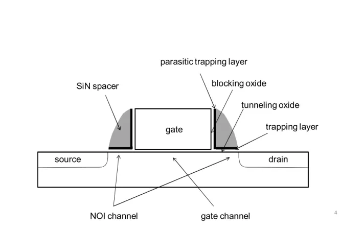
SONOS memories have been developed as two-bit-per-cell operation for high density nonvolatile memory (NVM). Novel operating schemes and array designing offer improved performance and cell area, such as CHISEL and buried diffusion bit-line ,etc.[20] Nevertheless, such SONOS devices are facing difficulties while scaling down, such as two-bit operation and oxide-nitride-oxide down scaling. Recently, the use of SiN spacers as the charge trapping media has provided another means of these issues [21]. Fuduka et al.[22] reported SiN sidewall between silicon oxide spacer and polysilicon gate for NV applications. Jeng el al.[23] reported nonoverlapped implantation (NOI) devices with SiN spacer as trapping media. The NOI devices can be manufactured without additional masks and complex process such as ONO dielectrics. For two-bit operation, the trapping spacers are physically separated by the gate electrode and gate oxide, so the scaling risk of two-bit charge merging can be avoided in NOI devices. Furthermore, these advantages are attractive for embedded NVM applications in standard logic CMOS technologies to improve the system operation speed. We choose HfO2 and HfSiOx for trapping layer under the SiN spacer for these NVM devices. The structure is shown in Fig. 2-1.
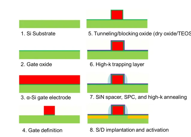
2.2 Device Fabrication
6
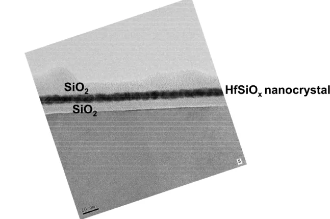
active region was defined by LOCOS process. Then 100Å gate oxide was grown in dry oxide furnace after RCA clean. Subsequently, 2000 Å amorphous silicon was deposited as gate electrode. After poly gate was defined and etched, 50 Å TEOS oxide or dry oxide was deposited as tunneling oxide and blocking oxide. We noted that the dry oxide can provide better interface quality than TEOS oxide as the tunneling oxide since the oxide is grown from single crystal silicon, but the dry oxide on the sidewall might show worse quality than TEOS oxide because the dry oxide is grown from amorphous silicon. After solid phase crystallization (SPC) was performed, 50 Å high-k trapping layer was deposited as trapping layer. SiN was then deposited and etched to form spacer, which has higher k value than SiO. Nanocrystal trapping layer was performed at 900℃ for 60 sec. Fig. 2-3 is the TEM picture of the nanocrystal, which is grown just for a capacitor structure and then annealed at the same conditions. Gate, source and drain were doped by a self-aligned ion implantation. After S/D formation, which was activated at 1000 ℃ for 10 sec, SiO passavation and AlSiCu metallization were performed to complete the spacer trap NVM. This gate stack contains only dray oxide and gate electrode, so this process is similar to the logic devices. For example, if the LDD and other dopants are implanted before spacer formation, this device might be used as logic device. The logic device structure is shown is Fig. 2-4.
2.3 Results and Discussion
2.3.1 Measurement of Threshold Voltage
The threshold voltage measurement is constant current method in Id-Vg curve. We observed that Id was limited at small Vd, due to the channel resistance under the spacer is large. Therefore, the drain voltage is applied at 2V in our Id-Vg measurement for threshold voltage.
7
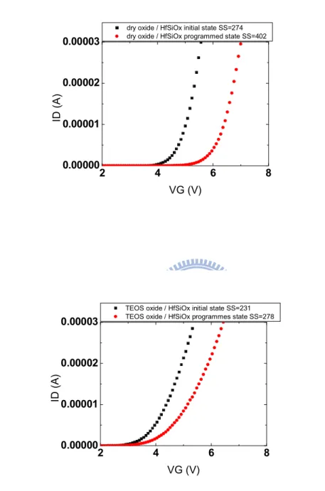
2.3.2 Drain Current vs Gate Voltage
The ID-VG curves are shown in Fig. 2-5(a),(b), and the characteristics is shown in Table 2-1. We choose 10V gate stress and 8V drain stress for 1ms to measure the programmed state. The subthreshold swing is about 200~300mV/decade at erase state. Because the region of the substrate under the spacer is not implanted as LDD source/drain, the channel under the spacer is more difficult to turn on than the channel under the gate electrode. Thus the subthreshold swing is large. After programmed, the channel under the spacer with larger resistance regress the subthreshold swing to 250~450mV/decade.
2.3.2 Programming Characteristics
2.3.2.1 Programming Mechanism
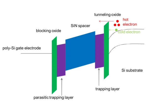
In this chapter, the programming scheme is executed by using channel hot electron injection (CHEI) to move charge in trapping layer, thus threshold voltage could be changed. Fig. 2-6 shows the hot electron injection scheme and band diagram in this spacer trap NVM. The electrons are hot because they are accelerated in the channel and heated into high-energy state. A part of the electrons owns energy which is higher than the barrier height of the SiO2/Si conduction band, so the electrons can surmount the barrier and are injected into the trapping layer.
2.3.2.2 Programming Properties
The program characteristics with different tunneling/blocking oxide are shown in Fig. 2-7. The TEOS oxide provides better programming speed at long stress due to the oxide quality above the NOI channel because the TEOS oxide contains more interface states than dry oxide grown from single crystal silicon and the TEOS oxide can provide more tunneling
8
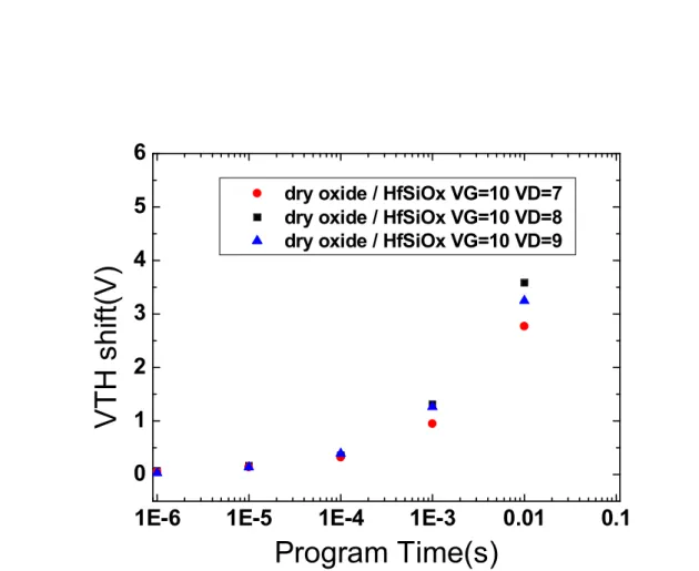
paths. The program characteristics with different gate bias are shown in Fig. 2-8. The programming speed is faster with the higher gate voltage because the charges are with more energy. Furthermore, the gate bias provides larger electric field and enhances the tunneling. The program characteristics with different drain bias are shown in Fig. 2-9. The programming speed isn’t corresponding to the drain voltage. We can see that the best programming efficiency isn’t with the largest drain voltage. There are two possible explanations. First, the distribution of the electrons in the spacer of smaller programming voltage might cause more threshold voltage shift. Second, the gate oxide might be destroyed at high programming voltage.
2.3.3 Erasing Characteristics
2.3.3.1 Erasing Mechanism
The erase scheme is executed by band-to-band hot hole, which is shown in Fig. 2-10. The drain is applied on a positive voltage while the gate is applied on a negative voltage. The holes have high energy while they reach the oxide are injected in to the trapping layer to neutralize the trapped electrons and the threshold voltage decreases.
2.3.3.2 Erasing Properties
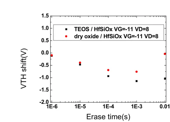
Fig. 2-11 shows the erase characteristics with different tunneling/blocking oxide after pre-programming. 1V threshold voltage shift pre-programming. The pre-programming time is about 0.1ms and the pre-programming gate/drain voltages are 10V/8V. The TEOS oxide on sidewall provides better blocking ability for gate injection than amorphous-Si dry oxide. Due to the gate injection from gate into nanocrystal at sidewall of poly gate, we observe that the erase curve raise after 1ms. Fig. 2-12 shows the erase characteristics with different gate bias. Before 10μs, 10V gate voltage provides little better erase speed, but the gate injection is also
9
enhanced at higher gate voltage after 0.1ms. Fig. 2-13 shows the erase characteristics with different drain bias. Similar to programming characteristics, we can see that the best erase efficiency isn’t with the largest drain voltage, due to the electric field profile and the trap position.
2.3.4 Retention Characteristics
2.3.4.1 Retention mechanism
Retention is an important reliability issue for non-volatile memory. The de-trapping of the
electrons trapped in the trapping layer decreases the threshold voltage, thus the window between program-state and erase-state becomes narrower. Normally, there’s more charge loss at higher temperature.
2.3.4.2 Retention Properties
As shown in Fig. 2-14(a),(b) , after 1.5V of threshold voltage shift by programming, the retention properties is almost remain at the same threshold voltage for 1000s at 25℃. After 1000s the threshold voltage even increases with waiting time. Like most retention characteristics, the retention curves for 125℃ are under 25℃, so the charge loss is more at higher temperature.
However, it’s not a typical trend in a retention curve for NVM that the threshold voltages increase
by time. The threshold voltage drops or remains at first 1000s, and then some of the threshold voltages are raised after. One possible reason is that the device might be programmed while measuring ID-VG curves. But after measuring ID-VG for 20 cycles at 0s and 10000s, the
threshold voltage doesn’t change as the retention curve. So this non-typical trend isn’t caused
by the programming effect at the ID-VG measurement after each waiting time. The mechanism
of the threshold voltage raising may be caused by the thermal migration of the charge in nitride spacer. As shown in Fig. 2-15, the migration of trapped charges changes the threshold
10 voltage. According to the equation,
, where Q0 is the oxide trapped charge, C0 is the oxide capacitance, d is oxide thickness, and
x0 is the distance from gate electrode to trapped charge. While the trapped electrons move to
the substrate, the flat-band voltage is affected more due to the increasing of x0.
2.3.5 Disturbance Characteristics
2.3.5.1 Disturbance Mechanism
The read disturbance takes place under the applied stress while reading the cell. The applied read voltage might turn on the channel or enhances tunneling to make electrons in the substrate into trapping layer and then the threshold voltage changes. Memory cells are often put in arrays to reduce the memory area and to simplify outside electric circuits. Therefore, the drain disturbance and gate disturbance need to be considered while neighboring cells especially un-programmed cells are stressed during some cell is being programmed. Fig. 2-16 shows the schematic circuitry of a memory array. During programming cell A, gate disturbance occurs in the cell B and same for those cells connected with the same word-line because the gate stress is applied to the same word-line (WL). This is called gate disturbance. During programming cell A, drain disturbance occurs in the cell C and same for those cells connected with the same bit-line because the drain stress is applied to the same bit-line (BL). This is called drain disturbance.
2.3.5.2 Disturbance Properties
Fig. 2-17~19 show the read, gate, and drain disturbance characteristic, respectively. The
11
disturbance. After 100s of stress, electrons are programmed into the trapping layer due to the high gate voltage in gate disturbance measurement, high drain voltage in drain disturbance measurement, and the channel which the carriers are “not so hot” with lower energy than the programming operation causes read disturb. And the dry oxide provides better blocking ability than the TEOS oxide above the NOI channel.
2.4 Summary
The programming speed of these devices shows programming properties by CHE programming mechanism. However, the erase saturation limits the erase properties. The retention is good, but the charge injected into the nitride spacer redistribution make the threshold voltage increase by waiting time. The disturbance curves show that these devices are a little programmed after 100s gate/drain/read stress.
12
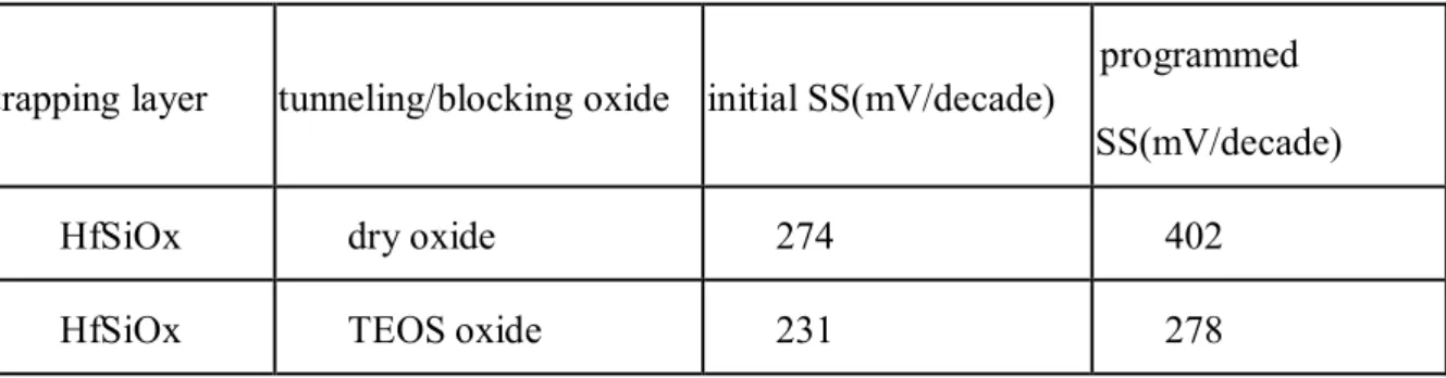
trapping layer tunneling/blocking oxide initial SS(mV/decade)
programmed SS(mV/decade)
HfSiOx dry oxide 274 402
HfSiOx TEOS oxide 231 278
13
source drain
gate
gate channel NOI channel
parasitic trapping layer blocking oxide
tunneling oxide SiN spacer
trapping layer
4
14
1. Si Substrate
2. Gate oxide
3. α-Si gate electrode
4. Gate definition
5. Tunneling/blocking oxide (dry oxide/TEOS)
6. High-k trapping layer
7. SiN spacer, SPC, and high-k annealing
8. S/D implantation and activation
15
SiO
2SiO
2HfSiO
xnanocrystal
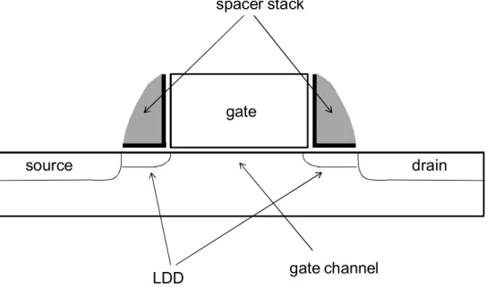
16 source drain gate gate channel LDD spacer stack
Fig. 2-4 structure of logic device with similar fabrication process of nonoverlapped implantation nonvolatile memory
17 (a) 2 4 6 8 0.00000 0.00001 0.00002 0.00003
dry oxide / HfSiOx initial state SS=274 dry oxide / HfSiOx programmed state SS=402
ID ( A ) VG (V) (b) 2 4 6 8 0.00000 0.00001 0.00002 0.00003
TEOS oxide / HfSiOx initial state SS=231 TEOS oxide / HfSiOx programmes state SS=278
ID
(A
)
VG (V)
Fig. 2-5 ID-VG curves of two states with (a) dry oxide (b) TEOS oxide as the tunneling/blocking oxide
18 hot electron tunneling oxide blocking oxide SiN spacer trapping layer parasitic trapping layer
poly-Si gate electrode
Si substrate
cold electron
19
1E-6 1E-5 1E-4 1E-3 0.01 0.1
0 1 2 3 4 5 TEOS / HfSiOx VG=9 VD=8 dry oxide / HfSiOx VG=9 VD=8
V
T
H
s
h
if
t(
V
)
Program Time(s)
20
1E-6 1E-5 1E-4 1E-3 0.01 0.1
0 1 2 3 4 5 6
dry oxide / HfSiOx VG=8 VD=8 dry oxide / HfSiOx VG=9 VD=8 dry oxide / HfSiOx VG=10 VD=8
V
T
H
s
h
if
t(
V
)
Program Time(s)
21
1E-6
1E-5
1E-4
1E-3
0.01
0.1
0
1
2
3
4
5
6
dry oxide / HfSiOx VG=10 VD=7 dry oxide / HfSiOx VG=10 VD=8 dry oxide / HfSiOx VG=10 VD=9
VT
H
s
h
if
t(V)
Program Time(s)
22 h+ tunneling oxide blocking oxide SiN spacer trapping layer parasitic trapping layer
poly-Si gate electrode
Si substrate
e
23
1E-6 1E-5 1E-4 1E-3 0.01
-2.0 -1.5 -1.0 -0.5 0.0 0.5 1.0 1.5 TEOS / HfSiOx VG=-11 VD=8 dry oxide / HfSiOx VG=-11 VD=8
V
T
H
s
h
if
t(
V
)
Erase time(s)
24
1E-6
1E-5
1E-4
1E-3
0.01
-2.0
-1.5
-1.0
-0.5
0.0
0.5
1.0
1.5
dry oxide / HfSiOx VG=-10 VD=8
dry oxide / HfSiOx VG=-11 VD=8
dry oxide / HfSiOx VG=-12 VD=8
V
T
H
sh
if
t(
V
)
Erase time(s)
25
1E-6
1E-5
1E-4
1E-3
0.01
-2.0
-1.5
-1.0
-0.5
0.0
0.5
1.0
1.5
dry oxide / HfSiOx VG=-12 VD=8
dry oxide / HfSiOx VG=-12 VD=9
dry oxide / HfSiOx VG=-12 VD=10
V
T
H
s
h
ift(
V
)
Erase time(s)
Fig. 2-13 erasing characteristics with different drain bias .
26
10
100
1000
10000
0
1
2
dry oxide / HfSiOx 25C
dry oxide / HfSiOx 125C
V
T
H
s
h
if
t
(V
)
Wait time(s)
(b)10
100
1000
10000
0
1
2
TEOS / HfSiOx 25C TEOS / HfSiOx 125CV
T
H
s
h
if
t
(V
)
Wait time(s)
Fig. 2-14 retention characteristics with (a)dry oxide (b)TEOS oxide as the tunneling/blocking oxide
27 (a)
(b)
28
A
C
B
29 (a)
1
10
100
1000
-0.3 -0.2 -0.1 0.0 0.1 0.2 0.3 0.4 0.5 0.6 0.7 0.8 0.9dry oxide / HfSiOx VG=4 VD=2
V
T
H
s
h
if
t(
V
)
Stress time(s)
(b)1
10
100
1000
-0.3 -0.2 -0.1 0.0 0.1 0.2 0.3 0.4 0.5 0.6 0.7 0.8 0.9 TEOS / HfSiOx VG=4.8 VD=2V
T
H
s
h
if
t(
V
)
Stress time(s)
Fig. 2-17 read disturbance characteristics with (a)dry oxide (b)TEOS oxide as tunneling/blocking oxide
30 (a)
1
10
100
1000
-0.3 -0.2 -0.1 0.0 0.1 0.2 0.3 0.4 0.5 0.6 0.7 0.8 0.9dry oxide / HfSiOx VG=10
V
T
H
s
h
if
t(
V
)
Stress time(s)
(b)1
10
100
1000
-0.3 -0.2 -0.1 0.0 0.1 0.2 0.3 0.4 0.5 0.6 0.7 0.8 0.9 TEOS / HfSiOx VG=10V
T
H
sh
if
t(
V
)
Stress time(s)
Fig. 2-18 gate disturbance characteristics with (a)dry oxide (b)TEOS oxide as tunneling/blocking oxide
31 (a)
1
10
100
1000
-0.3 -0.2 -0.1 0.0 0.1 0.2 0.3 0.4 0.5 0.6 0.7 0.8 0.9dry oxide / HfSiOx VD=8
VT
H
sh
if
t(V)
Stress time(s)
(b)1
10
100
1000
-0.3 -0.2 -0.1 0.0 0.1 0.2 0.3 0.4 0.5 0.6 0.7 0.8 0.9 TEOS / HfSiOx VD=8VT
H
sh
if
t(V)
Stress time(s)
Fig. 2-19 drain disturbance characteristics with (a)dry oxide (b)TEOS oxide as tunneling/blocking oxide
32
Chapter 3
Characteristics of Segmented n-MOSFET
3.1 Introduction
Recently, body-tied FinFETs built on bulk silicon (Si) wafer have been demonstrated experimentally [24][25][26] and have shown several advantages over SOI FinFETs while keeping nearly the same scaling down characteristics [27] as those of SOI FinFETs. The device is called bulk FinFETs to differentiate from SOI FinFETs. The bulk FinFETs have been considered as a promising candidate for future CMOS technology because the devices have several advantages such as low cost, low defect density, no floating body effect, high heat transfer rate to the substrate, and nearly the same process flow as conventional bulk CMOS technology.
3.2 Device Fabrication
The fabrication process steps are illustrated in Fig. 3-1. First, a bulk silicon wafer was defined active region by shallow trench isolation process. After well formation and threshold voltage-adjust ion implantation, the STI oxide was recessed by a small amount for split conditions. Then the poly gate was formed and defined, just prior to the gate oxide oxidation. As a result, a tri-gate structure was achieved. After LDD and pocket implants, gate spacer was formed. Then the source/drain and gate was implants as self-alignment. The activation process and metal silicidation were the final steps of the front-end-of-line process. Fig. 3-2 is the TEM picture of the FIN structure.
33
3.3 Results and Discussion
3.3.1 Device Structure of 3-point SegFETs
The SegFET devices were fabricated by 28 nm CMOS process, for different gate lengths, gate widths, and FIN numbers. The thickness of the gate oxide is about 12~20 Å, and the gate-to-S/D contact length is most 30 nm without body contacts. The diagram of top view of the devices is shown in Fig. 3-3.
3.3.2 Drain Current vs. Gate Voltage Curve
Fig. 3-4 shows the ID-(VG-VTH) curves for the SegFet devices, where VTH is
extracted by constant drain current method. Ion-Ioff ratio reaches 108. And the curve between
each STI-recess thickness is near to each other in the same gate length, so the channel properties are nearly beside threshold voltage. We noted that Ion/(W/L) increases with channel length. The trend is not typical as the short channel effect for short channel length devices. It will be explained after.
3.3.3 FIN Number and Electrical Properties
As shown in Fig. 3-5, the on current, which is the drain current divided by the FIN number, isn’t much dependent on the FIN number. Fig. 3-6 shows that the threshold voltage is also independent with the FIN number. So we assume that the interactions between the neighbor depletion regions which are parallel. The uniformity of the devices is good, since each FIN shows similar properties.
3.3.4 Drain Current vs. Gate Length
34
conditions. We conjecture that the pocket implant concentration is too high that the dopants diffuses to the channel surface to increase the threshold voltage or diffuses to the source/drain LDD to increase the series resistance of source/drain. For the same top view width (Wtop), which is the real area of the chip, more recess devices provide larger on current, so the STI recess can maintain the driving current while scaling down. However, the on current of more STI-recess devices with the same real width (Wtotal=Wtop+2*STI recess) provides less normalized on current. Thus, the mobility of the devices with more STI-recess thickness decreases. It might be due to the pocket implant, and the sidewall-channel mobility degrades for more channel dopant concentration.
3.3.5 Threshold Voltage and Subthreshold Swing vs. Gate
length
As shown in Fig. 3-8, the threshold voltage increases as the channel length decreases, especially at the sub-100nm region. The short channel effect isn’t the major effect at this region. Therefore, we calculated the subthreshold swing of these devices. Fig. 3-9 shows the subthreshold swing characteristics. The subthreshold swing curves show that the subthreshold swing of the shorter device is worse, and it’s corresponding to the short effect. It’s due to that the source/drain and pocket implantation profile couldn’t match good, thus the series resistance dominates the threshold voltage. Therefore, the on current and threshold voltage trend don’t show the short channel effect. Also, the subthreshold swing degenerates at short channel region because of the pocket implant profile.
We noted the subthreshold swing characteristics of the device with more STI recess thickness in smaller in Fig. 3-9. Obviously the “deeper” devices, which own more STI recess thickness, have smaller threshold voltages, as shown in Fig. 3-8. Fig. 3-10 is the scheme of different STI recess thickness. The deeper FINs’ depletion region from sidewall enhanced
35
more volume of the FIN, thus the the inversion layer forms earlier than the device with less STI recess thickness. Therefore, the ”fully-depleted likely” mechanism decreased the threshold voltage and improve the subthreshold swing.
3.3.6 Device structure of 4-point Devices
To verify the fully-depleted effect, we measured other test structures, which have only one FIN but 4-point contacts, for body effect. The diagram of top view of the devices is shown in Fig. 3-11.
3.3.7 Threshold Voltage vs. Gate length on 4-point Devices
Similar to former devices, the threshold voltages decreases as the gate length increases, due to the pocket implant, as shown in Fig. 3-12. Also, 30nm-STI-recess devices own smaller threshold voltage, due to the corner effect and the sidewall depletion region.
3.3.8 Threshold Voltage vs. Gate width on 4-point Devices
Fig. 3-13 shows the relation between the channel width and threshold voltage. Certainly, the threshold voltage of more recess devices is smaller. Otherwise, the threshold voltage increases as the channel width, due to the top-sidewall channel ratio. As shown in Fig. 3-14 the sidewall channel affects more at narrower width, so the threshold voltage is suppressed.
3.3.9 Body Effect on 4-point Devices
To verify that the depletion region of sidewall helps the inversion of channel, we measured the body effect. The threshold voltage shift is the difference of threshold voltage
36 ,
the threshold voltage will increase with VSB . Fig. 3-15 shows the threshold shift-channel
width curves. In deep-recess devices, the body voltage is blocked by the sidewall depletion region, so the threshold voltage shift is not much as shallow-recess devices. Similarly, the body voltage is blocked in the devices with narrower gate width.
3.3.10 Kink Effect
Fig. 3-16 shows the ID-VD curves of SegFET 3-point devices. The kink effect is obvious in 10 and 15 nm-recess devices but not obvious in 30nm-recess devices. The kink effect usually takes place at the partially-depleted devices on SOI wafer, but not in fully-depleted devices. According to Fig. 3-10, we may say that the depletion region of sidewall help the inversion earlier than conventional inversion mechanism of planar devices, so deep-STI-recess devices shows “fully depleted likely” characteristics.
3.4 Summary
The recess of STI oxide improves some characteristics of the devices. The operation speed is improved by the recess because the subthreshold swing is improved. However, the doping profiles of the LDD and pocket implant don’t match well so we couldn’t compare the short channel effect. We also noted that the sidewall depletion region affects the threshold voltage by corner effect. After measuring the body effect, the body voltage is blocked, and is dependent to the recess thickness and FIN width. Besides, the ID-VD curves also show that the FIN structure may cause fully depleted characteristics, like the devices on SOI wafer.
37 •Top view •Cross-section along gate width direction •Cross-section along gate length direction •Top view •Cross-section along gate width direction •Cross-section along gate length direction
•1. Si substrate
•2. Shallow trench isolation
•3. STI oxide recess
•4. Gate oxide
•6. LDD & pocket implantation
•7. Spacer formation
•8. S/D implantation
•5. Poly–Si gate electrode and gate definition
38
Si FIN
STI oxide
Poly-Si
Silicide
contact
39 1 2 3 … N W
Wtop=N*W
Wtotal=N*(W+2*STI recess )
G
S
D
L40 (a) -1.0 -0.5 0.0 0.5 1.0 1.5 1E-14 1E-13 1E-12 1E-11 1E-10 1E-9 1E-8 1E-7 1E-6 1E-5 W=30 L=27 N=20 STI recess=10 W=30 L=27 N=20 STI recess=15 W=30 L=27 N=20 STI recess=30
ID/
(W
/L)
(A
)
VG-VTH (V)
(b) -1.0 -0.5 0.0 0.5 1.0 1.5 1E-14 1E-13 1E-12 1E-11 1E-10 1E-9 1E-8 1E-7 1E-6 1E-5 W=30 L=27 N=20 STI recess=10 W=30 L=50 N=20 STI recess=10 W=30 L=100 N=20 STI recess=10 W=30 L=200 N=20 STI recess=10 W=30 L=1000 N=20 STI recess=10ID
/(
W
/L
)
(
A
)
VG-VTH (V)
41 (a) 0 5 10 15 20 1E-5 2E-5 3E-5 4E-5 STI recess=10, W=30, L=100 STI recess=10, W=30, L=55 STI recess=10, W=30, L=45 STI recess=10, W=30, L=32 ID /( W /L ) (A ) N (b) (c) 0 5 10 15 20 1E-5 2E-5 3E-5 4E-5 STI recess=15, W=30, L=100 STI recess=15, W=30, L=55 STI recess=15, W=30, L=45 STI recess=15, W=30, L=35 ID /( W/ L ) (A ) N 0 5 10 15 20 1E-5 2E-5 3E-5 4E-5 STI recess=30, W=30, L=100, STI recess=30, W=30, L=55 STI recess=30, W=30, L=45 STI recess=30, W=30, L=32 ID /( W /L ) (A ) N
42 (a) 0 5 10 15 20 0.2 0.4 0.6 W=30, L=32, STI recess=10 W=30, L=45, STI recess=10 W=30, L=55, STI recess=10 W=30, L=100, STI recess=10 VT H ( V) N (b) 0 5 10 15 20 0.2 0.4 0.6 W=30, L=32, STI recess=15 W=30, L=45, STI recess=15 W=30, L=55, STI recess=15 W=30, L=100, STI recess=15 V T H ( V ) N (c) 0 5 10 15 20 0.2 0.4 0.6 W=30, L=32, STI recess=30 W=30, L=45, STI recess=30 W=30, L=55, STI recess=30 W=30, L=100, STI recess=30 V T H ( V ) N
43 (a)
10
100
1000
1E-5
W=30 STI recess=10 N=20 W=30 STI recess=15 N=20 W=30 STI recess=30 N=20Io
n
/(W
to
p
/L
)
(A
)
L (nm)
(b)10
100
1000
1E-5
STI recess=10,W=30,N=20 STI recess=15,W=30,N=20 STI recess=30,W=30,N=20Io
n
/(
W
to
ta
l/
L
)
(A
)
L (nm)
Fig. 3-7 on current vs. gate length which on current is normalized by (a) top gate width (b) total gate width
44
10
100
1000
0.10
0.15
0.20
0.25
0.30
0.35
0.40
0.45
0.50
W=30, STI recess=10, N=20 W=30, STI recess=15, N=20 W=30, STI recess=30, N=20V
T
H
(
V
)
L (nm)
45
100
1000
65
70
75
80
85
90
95
STI recess =10 W=30 N=20 STI recess= 15 W=30 N=20 STI recess= 30 W=30 N=20S
S
(
V
/d
e
c
a
d
e
)
L(nm)
46
47 W
G
S
D
LB
48
10
100
1000
0.0
0.1
0.2
0.3
0.4
0.5
0.6
0.7
0.8
0.9
1.0
W=500, STI recess=10 W=500, STI recess=15 W=500, STI recess=30V
T
H
(
V
)
L (nm)
49
100
1000
10000
0.0
0.1
0.2
0.3
0.4
0.5
0.6
0.7
0.8
0.9
1.0
L=50, STI recess=10
L=50, STI recess=15
L=50, STI recess=30
V
T
H
(V
)
W (nm)
50
51 100 1000 10000 0.0 0.1 0.2 0.3 0.4 0.5 L=50, STI recess=10 L=50, STI recess=15 L=50, STI recess=30
V
T
H
s
h
if
t
(V
)
W (nm)
52 (a) 0.0 0.5 1.0 1.5 2.0 2.5 3.0 0.0000 0.0005 0.0010 0.0015 0.0020 0.0025 0.0030 0.0035 0.0040 ID ( A ) VD (V) STI=10 W=30 L=27 N=20 VG=0 STI=10 W=30 L=27 N=20 VG=0.5 STI=10 W=30 L=27 N=20 VG=1 STI=10 W=30 L=27 N=20 VG=1.5 (b) 0.0 0.5 1.0 1.5 2.0 2.5 3.0 0.0000 0.0005 0.0010 0.0015 0.0020 0.0025 0.0030 0.0035 0.0040 STI=15 W=30 L=27 N=20 VG=0 STI=15 W=30 L=27 N=20 VG=0.5 STI=15 W=30 L=27 N=20 VG=1 STI=15 W=30 L=27 N=20 VG=1.5 ID (A ) VD (V) (c) 0.0 0.5 1.0 1.5 2.0 2.5 3.0 0.0000 0.0005 0.0010 0.0015 0.0020 0.0025 0.0030 0.0035 0.0040 STI=30 W=30 L=27 N=20 VG=0 STI=30 W=30 L=27 N=20 VG=0.5 STI=30 W=30 L=27 N=20 VG=1 STI=30 W=30 L=27 N=20 VG=1.5 ID ( A ) VD (V)
53
Chapter 4
Characteristics of Segmented p-MOSFET
4.1 Introduction
In chapter 3, the characteristics of Si-bulk segmented n-MOSFET were shown. We’ll show the characteristics of Si-bulk segmented p-MOSFET with the same CMOS process.
4.2 Device Fabrication
As last chapter, the fabrication process steps are illustrated in Fig. 3-1. First, a bulk silicon wafer was defined active region by shallow trench isolation process. After well formation and threshold voltage-adjust ion implantation, the STI oxide was recessed by a small amount for split conditions. Then the poly gate was formed and defined, just prior to the gate oxide oxidation. As a result, a tri-gate structure was achieved. After LDD and pocket implants, gate spacer was formed. Then the source/drain and gate was implants as
self-alignment. The activation process and metal silicidation were the final steps of the front-end-of-line process.
4.3 Results and Discussion
4.3.1 Device Structure of 3-point SegFETs
The same as NMOS chapter 2, the P-SegFET devices were fabricated by 28 nm CMOS process, for different gate lengths, gate widths, and FIN numbers. The thickness of the gate oxide is about 12~20 Å, and the gate-to-S/D contact length is most 30 nm without body contacts. The diagram of top view of the devices is shown in Fig. 3-3.
54
4.3.2 Drain Current vs. Gate Voltage Curve
Fig. 4-1 shows the ID-(VG-VTH) curves for the SegFet devices, where VTH is
extracted by constant drain current method. Ion-Ioff ratio reaches 108. And the curve between
each STI-recess thickness is near to each other in the same gate length, so the channel properties are nearly beside threshold voltage. We noted that Ion/(W/L) increases with channel length. The trend is not typical as the short channel effect for short channel length devices, the same as NMOS devices.
4.3.3 FIN Number and Electrical Properties
As shown on Fig. 4-2, Ion, which is the drain current divided by the FIN number, isn’t much dependent on the FIN number. Fig. 4-3 shows the threshold voltage is also independent to the FIN number. So we assume that the interaction between the neighbor depletion regions which are parallel. The uniformity of the devices is good, since each FIN shows similar properties.
4.3.4 Drain Current vs. Gate Length
In Fig. 4-4 , the normalized Ion is small at short channel region for each STI-recess conditions. We conjecture that the pocket implant concentration is too high that the dopants diffuses to the channel surface to increase the threshold voltage or diffuses to the source/drain LDD to increase the series resistance of source/drain. For the same top view width (Wtop), which is the real area of the chip, more recess devices provide larger on current, so the STI recess can maintain the driving current while scaling down. However, the on current of more STI-recess devices with the same real width (Wtotal=Wtop+2*STI recess) provides less normalized on current. Thus, the mobility of the devices with more STI-recess thickness decreases. It might be due to the pocket implant, and the sidewall-channel mobility degrades
55 for more channel dopant concentration.
4.3.5 Threshold Voltage and Subthreshold Swing vs. Gate
length
As shown in Fig. 4-5, the threshold voltage increases as the channel length decreases, especially at the sub-100nm region. The short channel effect isn’t the major effect at this region. Therefore, we calculated the subthreshold swing of these devices. Fig. 4-6 shows the subthreshold swing characteristics. The subthreshold swing curves show that the subthreshold swing of the shorter device is worse, and it’s corresponding to the short effect. It’s due to that the source/drain and pocket implantation profile couldn’t match good, thus the series resistance dominates the threshold voltage. Therefore, the on current and threshold voltage trend don’t show the short channel effect. Also, the subthreshold swing degenerates at short channel region because of the pocket implant profile.
We noted the subthreshold swing characteristics of the device with more STI recess thickness in smaller in Fig. 4-6. Obviously the “deeper” devices, which own more STI recess thickness, have smaller threshold voltages, as shown in Fig. 4-5. Like NMOS, Fig. 3-10 is the scheme of different STI recess thickness. The deeper FINs’ depletion region from sidewall enhanced more volume of the FIN, thus the inversion layer forms earlier than the device with less STI recess thickness. Therefore, the ”fully-depleted likely” mechanism decreased the threshold voltage and improve the subthreshold swing.
4.3.6 Device structure of 4-point Devices
To verify the fully-depleted effect, we measured other test structures, which have only one FIN but 4-point contacts, for body effect. The diagram of top view of the devices is shown in Fig. 3-12.
56
4.3.7 Threshold Voltage vs. Gate length on 4-point Devices
Similar to NMOS devices, the threshold voltages decreases as the gate length increases, due to the pocket implant, as shown in Fig. 4-7. Also, 30nm-STI-recess devices own smaller threshold voltage, due to the corner effect and the sidewall depletion region.4.3.8 Threshold Voltage vs. Gate width on 4-point Devices
Fig. 4-8 shows the relation between the channel width and threshold voltage. Certainly, the threshold voltage of more recess devices is smaller. Otherwise, the threshold voltage increases as the channel width, due to the top-sidewall channel ratio. As shown in Fig. 3-14, the sidewall channel affects more at narrower width, so the threshold voltage is suppressed.
4.3.9 Body Effect on 4-point Devices
To verify that the depletion region of sidewall helps the inversion of channel, we measured the body effect. The threshold voltage shift is the difference of threshold voltage
between |VSB|=0V and |VSB|=2V. According to the Eq.
The threshold voltage will increase with |VSB|. Fig. 4-9 shows the threshold shift-channel
width curves. In deep-recess devices, the body voltage is blocked by the sidewall depletion region, so the threshold voltage shift is not much as shallow-recess devices. Similarly, the body voltage is blocked in the devices with narrower gate width.
57
The segmented p-MOSFET has similar properties to segmented n-MOSFET. The recess thickness of STI oxide improves some characteristics of the devices. The operation speed is improved by the recess because the subthreshold swing is improved. However, the doping profiles of the LDD and pocket implant don’t match well so we couldn’t compare the short channel effect. We also noted that the sidewall depletion region affects the threshold voltage by corner effect. After measuring the body effect, the body voltage is blocked, and is dependent to the recess thickness and FIN width. This phenomenon shows that the FIN structure may cause fully depleted characteristics, like the devices on SOI wafer.
58 (a) -1.0 -0.5 0.0 0.5 1.0 1.5 1E-14 1E-13 1E-12 1E-11 1E-10 1E-9 1E-8 1E-7 1E-6 1E-5 W=30, L=27, N=20, STI recess=10 W=30, L=27, N=20, STI recess=15 W=30, L=27, N=20, STI recess=30
ID
/(
W/
L
)
(A
)
|VG-VTH| (V)
(b) -1.0 -0.5 0.0 0.5 1.0 1.5 1E-14 1E-13 1E-12 1E-11 1E-10 1E-9 1E-8 1E-7 1E-6 1E-5 W=30, L=27, N=20, STI recess=10 W=30, L=50, N=20, STI recess=10 W=30, L=100, N=20, STI recess=10ID
/(
W
/L
)
(A
)
|VG-VTH| (V)
59 (a) 0 5 10 15 20 1E-5 STI recess=10, W=30, L=32 STI recess=10, W=30, L=45 STI recess=10, W=30, L=55 STI recess=10, W=30, L=100 ID/ (W /L ) ( A ) N (b) 0 5 10 15 20 1E-5 STI recess=15, W=30, L=32 STI recess=15, W=30, L=45 STI recess=15, W=30, L=55 STI recess=15, W=30, L=100 ID /( W /L) ( A ) N (c) 0 5 10 15 20 1E-5 STI recess=30, W=30, L=32 STI recess=30, W=30, L=45 STI recess=30, W=30, L=55 STI recess=30, W=30, L=100 ID /( W /L ) ( A ) N
60 (a) 0 5 10 15 20 0.2 0.3 0.4 0.5 0.6 STI recess=10, W=30, L=32 STI recess=10, W=30, L=45 STI recess=10, W=30, L=55 STI recess=10, W=30, L=100 V T H ( V ) N (b) 0 5 10 15 20 0.2 0.3 0.4 0.5 0.6 STI recess=15, W=30, L=32 STI recess=15, W=30, L=45 STI recess=15, W=30, L=55 STI recess=15, W=30, L=100 V T H ( V ) N (c) 0 5 10 15 20 0.2 0.3 0.4 0.5 0.6 STI recess=30, W=30, L=32 STI recess=30, W=30, L=45 STI recess=30, W=30, L=55 STI recess=30, W=30, L=100 V TH ( V ) N
61 (a)
10
100
1000
1E-5
STI recess = 10, W=10, N=20STI recess = 15, W=10, N=20 STI recess = 30, W=10, N=20
Io
n
/
(W
to
p
)/
L
(
A
)
L (nm)
(b)10
100
1000
1E-5
STI recess = 10, W=10, N=20 STI recess = 15, W=10, N=20 STI recess = 30, W=10, N=20Io
n
/
(W
to
ta
l)
/L
(
A
)
L (nm)
Fig. 4-4 on current vs. gate length which on current is normalized by (a) top gate width (b) total gate width
62
100
1000
0.2
0.3
0.4
0.5
STI recess=10, W=30, N=20 STI recess=15, W=30, N=20 STI recess=30, W=30, N=20|V
T
H
|
(V
)
L (nm)
63
100
1000
65
70
75
80
85
90
95
100
S
S
(
m
V
/d
e
c
a
d
e
)
L (nm)
STI recess=10,W=30,N=20 STI recess=15,W=30,N=20 STI recess=30,W=30,N=2064
10
100
1000
0.0 0.1 0.2 0.3 0.4 0.5 0.6 0.7 0.8 0.9 1.0 W=500, STI recess=10 W=500, STI recess=15 W=500, STI recess=30|V
T
H
|
(V
)
L (nm)
65
100
1000
10000
0.0
0.1
0.2
0.3
0.4
0.5
0.6
0.7
0.8
0.9
1.0
L=50, STI recess=10
L=50, STI recess=15
L=50, STI recess=30
|V
T
H
|(
V
)
W (nm)
66