All-optical switching behaviors in an
all-semiconductor nonlinear loop device
Jiun-Haw Lee, Jyh-Yang Wang, C. C. Yang,*and Yean-Woei Kiang
Department of Electrical Engineering, Graduate Institute of Electro-Optical Engineering, and Graduate Institute of Communication Engineering, National Taiwan University, 1 Roosevelt Road, Section 4, Taipei, Taiwan
Received November 27, 2000; revised manuscript received March 12, 2001
Feasibility of pulsed-signal operation of all-optical self-switching and cross switching in an all-semiconductor optical-amplifier nonlinear optical loop device is reported. The device, based on a GaAs/AlGaAs quantum-well epitaxial structure, has dimensions of 0.6 mm⫻1.3 mm and a latency of 49.2 ps. It is composed of a loop am-plifier, a multimode interference waveguide amplifier (MMIWA), an input leg, and an output leg. The func-tions of the MMIWA include input/output power splitting and nonlinear coupling. Those of the loop include signal amplification, rearrangement of the field distribution in the MMIWA, and asymmetric gain/phase modu-lation between the two counterpropagating signals. With these functions combined, quite efficient power-dependent switching was implemented. Numerical-simulation results agreed well in trends with experimen-tal data. From the results of output pulse width and the pump–probe measurements, it is expected that high-speed operation of the device for all-optical modulation and multiplexing/demultiplexing is feasible. © 2001 Optical Society of America
OCIS codes: 230.1150, 190.5940.
1. INTRODUCTION
All-optical devices based on nonlinear Sagnac interferom-etry are attractive for high-speed communications and signal processing. Basically, such a device includes a loop structure for providing power-dependent phase/gain modulation and a 2 ⫻ 2 coupler for signal splitting/ combination. Hence the loop structure needs to contain a material for a certain nonlinear-optics mechanism. Ba-sically, when equal or unequal power splits into the two counterpropagating components of the loop, the compo-nents experience different gain/phase modulations. This difference determines the distribution of signal power be-tween the two output ports of the 2⫻ 2 coupler. Since the difference in gain/phase modulation is dependent on the input-power level, the aforementioned output-power distribution is controlled by the input power.
The development of this family of devices started with the proposal and the implementation of nonlinear optical loop mirrors1–3(NOLMs). A NOLM is an all-fiber device, including a fiber loop and a fiber coupler. The required nonlinear mechanism is the Kerr effect in the fiber loop. Because Kerr nonlinearity is relatively weak, the fiber loop is typically several hundred meters in length for cu-mulating self-phase modulation. To enhance optical non-linearity and reduce the loop length, a semiconductor op-tical amplifier (SOA) was asymmetrically inserted into the fiber loop.4 Since the nonlinear phase modulation in-duced by gain saturation in an SOA is much more effec-tive than that induced by the Kerr effect in fiber, the nonlinear-optics mechanism for the operation of such a nonlinear loop device relies on gain saturation in the SOA. Hence the fiber-loop length can be reduced to 0.5 m or shorter. Such a device has been used for teraHertz op-tical demultiplexing.5 However, the devices with fiber
are not only bulky but also have long latencies, which can
be as large as a few nanoseconds. To make a compact de-vice with a shorter latency, monolithic all-semiconductor loop devices were implemented. In such an implementa-tion, a SOA was inserted into a passive semiconductor waveguide loop. The loop was connected with a multi-mode interference waveguide amplifier (MMIWA), which served as the input/output coupler.6 The latency of this compact device was tremendously reduced. However, re-growth was required in fabricating this device that made the process complicated. Recently, we reported the fab-rication and cw-signal operation of an all-SOA nonlinear loop device.7,8 Besides the SOA loop, an MMIWA was used for closing the loop. With cw signals, efficient all-optical switching was observed. In cw operation the functions of the loop are to amplify the signals and to re-arrange the signal-field distribution in the lateral dimen-sion of the MMIWA. Such crucial functions combine with the nonlinear-coupling phenomena in the MMIWA for ef-ficient nonlinear-switching operation. Induced by gain saturation the nonlinear coupling in the MMIWA leads to power-dependent lateral-field distribution after propaga-tion.
In this paper we report the pulsed-signal operation and explain the function mechanisms of a similar device. The implementation of pulsed-signal operation implies a further step toward practical application of such a device. Also, we discuss the different operation mechanisms in
pulsed-signal operation. In this situation the
asymmetric-loop structure plays a crucial role. There-fore the observed power-dependent switching resulted from the combination effect of asymmetric gain/phase modulation in the loop and nonlinear coupling in the MMIWA. Efficient self-switching was observed. Nu-merical simulations showed the similar trends in switch-ing behaviors. To demonstrate on all-optical switching
function, the results of pump–probe experiments are pre-sented. The purpose of this paper is to demonstrate the feasibility and to shed some light on the operation prin-ciples of such a device configuration. Efforts are still needed to make it practical in use. For instance, such a device based on InGaAsP/InP structures with operation wavelength near 1550 nm is required for communication applications. In Section 2 of this paper, device design, fabrication, and measurement procedures are described. The results of self-switching are discussed in Section 3. Then, numerical modeling and its results are presented in Section 4. The experimental results of the pump–probe measurements are given in Section 5. Finally, conclu-sions are drawn in Section 6.
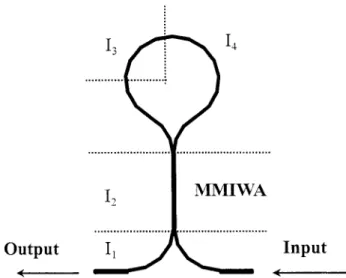
2. DEVICE DESIGN, FABRICATION, AND
MEASUREMENT PROCEDURES
The device configuration is similar to that previously reported7,8 except that the one-quarter and the
three-quarter sections of the loop are here divided for different injection currents (I3and I4, respectively). The top view
of the device is shown again in Fig. 1. Besides I3and I4
for the loop, the injection currents for the regions of MMIWA and the input/output portion are I2 and I1,
re-spectively. Good passivation was made for disconnecting the four injection areas. The epitaxial structure and fab-rication processes have been described in Ref. 8. Briefly, a GaAs/AlGaAs multiple-quantum-well structure was used. The peaks of electro-luminescence in the TE and the TM polarizations were 834 and 818 nm, respectively. Ridge waveguides with width 4m were formed for the loop and the input/output regions. Those with 8-m width were used for the MMIWA. A cryo-etching tech-nique was utilized to form vertical and smooth etched walls for low-loss curved waveguides.9 The radius of the loop was 300 m. The length of the MMIWA was 460 m. That of the input or output leg was ⬃300 m. The total length of the device (from the input end to the
out-put end) was 4.34 mm, corresponding to a latency of 49.2 ps. This is much shorter than those of the similar de-vices with fiber.
Figure 2 shows the experimental setup for self-switching. Pulses of 100-fs width from a mode-locked Ti:sapphire laser (Coherent, Mira 900) were first passed through a bandpass filter (a small monochromator) for se-lecting the required center wavelength and bandwidth of the input signal. The autocorrelation trace of the pulse after the filter is shown in Fig. 3. The full width at half-maximum (FWHM) of this signal pulse was ⬃1.4 ps. Figure 4 shows the spectra before the filter (I, dotted curve) and after the filter (II, solid curve) when the filter was arranged for an 834-nm signal. The signal wave-length after the filter can be tuned over the spectral range of the ficosecond pulse (⬃10 nm). It can be broadly tuned by varying the central wavelength of the ficosecond Ti:sapphire laser. The bandwidth of the signal after the filter was⬃2.5 nm, implying that the signal pulse was not transform limited.
Then, such signals were end coupled into the input leg of the device. A current pulse generator was used to pro-duce pulsed current of⬃1 kHz in repetition rate and 1% in duty cycle. The signals emerging from the output leg were passed through another bandpass filter for reducing amplified spontaneous-emission (ASE) noise. A lock-in amplifier was also used to increase the signal-to-noise ra-tio. Different from the cw operation, the optical signals were chopped in the pulsed case. Also, the pulsed injection-current repetition rate was set at twice the chop-per frequency. In the cw signal case the optical signals outside the injection-current window were almost com-pletely absorbed and made no contribution to the output power. However, in the pulsed-signal case, in the period without injection current, the absorption of a SOA could be saturated because of the high signal peak power. Hence the residual optical signals contributed to the out-put power and might interfere with the real operation of the device. This absorption-saturation effect needed to be removed. Meanwhile, the device acquired much ASE noise during current injection. This was to be removed for improving the signal-to-noise ratio.
Fig. 1. Layout of the all-semiconductor optical-amplifier Sagnac interferometer device. Electrode is divided into four discon-nected sections denoted by I1through I4.
Fig. 2. Experimental setup for self-switching operation with pulsed signals. Here, C, P,/2, f, and Det. represent chopper, polarizer, half-wave plate, chopping frequency, and detector, re-spectively.
As illustrated in Fig. 5, several procedures were con-ducted to eliminate the absorption-saturation effect and the ASE noise. Figure 5(a) shows the chopping windows of the lock-in amplifier. Optical signals were passed through the device in the ‘‘open’’ periods and stopped in the ‘‘close’’ periods. As shown in Fig. 5(b), the frequency of the electrical pulse train was set at twice the chopper frequency. The square windows represent the periods of electrical injection. The output signals directly from the device were sketched in Fig. 5(c). One can see that in the open periods, the signals include three parts: (1) ampli-fied pulses (the high peaks in the figure) during the time spans, in which both an optical signal and an injection current are present; (2) optical pulses with absorption saturation (the low peaks) when only optical signals exist; and (3) amplified spontaneous emission (the shaded rect-angular areas) whenever there is injection current. In
the close periods of Fig. 5(c), because optical signals were chopped, only ASE noise exists, as shown with the shaded areas. The lock-in amplifier performed a subtraction op-eration between the signals in the open and close periods. Hence after the lock-in amplifier operation, as shown in Fig. 5(d), ASE could be differentially filtered. Then, for eliminating the effect of absorption saturation, we set the SOA to be reverse biased with the same current pulse generator. As shown in Fig. 5(e), in this situation optical signals were almost completely absorbed. We then made a subtraction of output signals read from the lock-in am-plifier between the forward-bias [Fig. 5(d)] and reverse-bias [Fig. 5(e)] results. The subtraction result, as shown in Fig. 5(f), was free from the absorption-saturation effect. For studying cross-switching phenomena, optical pulses from the ficosecond Ti:sapphire laser were split into pump and probe signals. For either the pump or the probe path, after passing through a bandpass filter, a half-wave plate, and a polarizer, signals of different wave-lengths and/or polarization were end coupled into the in-put leg of the device. Time delay between the pump and the probe signals was controlled with a delay line that in-cluded a stepping-motor-controlled prism. Because it is difficult to conduct the procedures described above for re-moving the ASE and the absorption-saturation effect, the signal-to-noise ratio in cross-switching results might be degraded.
Fig. 3. Autocorrelation trace of the pulse after the tunable filter of the input end. It shows that the FWHM of the device input signal is⬃1.4 ps in width.
Fig. 4. Signal spectra before (curve I) and after (curve II) the tunable filter of the input end.
Fig. 5. Relations between (a) the chopping windows of the lock-in amplifier, (b) the electrical pulses, (c) the output optical signals with forward bias, (d) the optical signals after lock-in am-plifier operation, (e) the output optical signals with reverse bias, and (f) signals after the subtraction between the forward- and reverse-biased results.
3. EXPERIMENTAL RESULTS OF
SELF-SWITCHING
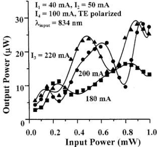
Figure 6 shows three sets of data revealing power-dependent switching when TE-polarized input signals at 834 nm (TE gain peak) were used. Note that in Figs. 6 through 10, the continuous curves are drawn to best fit the data points for guiding the eyes. The horizontal axis represents the average input power before entering the input leg. The input-coupling efficiency was estimated to be lower than 10%. In Fig. 6 the injection-current values of I1, I3, and I4 were fixed at 40, 200, and 100 mA,
re-spectively, leading to the injection-current density ratio of the one-quarter section over the three-quarter section of the loop, 6:1. The three curves correspond to the I2
val-ues (into the MMIWA region) at 25, 50, and 75 mA, re-spectively. One can see that significant nonlinear switch-ing occurs when I2 is sufficiently large. Generally
speaking, a larger I2 leads to a smaller switching power,
which could be defined as the input power leading to the first major maximum of output power (such as the maxi-mum at 0.6-mW input power for the case I2⫽ 50 mA). It
is noted that the input-power level in Fig. 6 is two orders of magnitude smaller than its counterpart in the cw sig-nal operation,8 confirming that the pulsed-signal opera-tion is much more efficient in all-optical switching. For instance, 0.5-mW switching power in the horizontal axis of Fig. 6 corresponds to a switching energy of only 330 fJ if 5% of input-coupling efficiency is assumed.
Figure 7 demonstrates three sets of data with I3varied
from 180 to 220 mA. In this figure, I1, I2, and I4 were
fixed at 40, 50, and 100 mA, respectively. The signal was still TE polarized with the center wavelength at 834 nm. A larger value of injection current in the one-quarter loop region means a larger gain and more asymmetry. Hence with increasing I3 the output power is increased and
switching power is decreased. In the case of I3
⫽ 200 mA an output-variation ratio of 2.75 (between in-put powers of 0.65 and 0.8 mW) was obtained. To inves-tigate the loop-asymmetry effect, I3⫹ I4 was fixed. In
Fig. 8 we show three sets of data when I1, I2, and I3
⫹ I4are fixed at 40, 50, and 300 mA, respectively. The I3 (I4) value is varied from 175 (125) to 225 (75) mA.
These variations mean that the ratio of injection-current density or gain constant between the one-quarter loop and the three-quarter loop is approximately 4:1, 6:1, and 9:1 for the three curves, respectively. One can see that the output power decreases with increasing I3or
decreas-ing I4, i.e., increasing the gain-constant ratio.
Mean-while, the switching power decreases with an increasing ratio, implying that the increase of loop asymmetry leads to more efficient nonlinear switching.
Then, Fig. 9 demonstrates the nonlinear-switching re-sults at different TE-signal wavelengths of 830, 834 (gain peak), and 838 nm. The values of the injection currents,
I1, I2, I3, and I4, are fixed at 40, 50, 200, and 100 mA,
respectively. Here, one can see that wavelength choice is quite important for efficient nonlinear switching. Effi-cient switching could be observed within 6 nm centered at the gain peak. In Fig. 10 we show three sets of data of TM-polarized signals with the same values of injection currents as those in Fig. 9. The wavelength was varied
Fig. 6. Output power as a function of average input power (TE polarized) with different I2levels.
Fig. 7. Output power as a function of average input power (TE polarized) with different I3levels.
Fig. 8. Output power as a function of average input power (TE polarized) with different (I3,I4) values.
from 818 nm (TM gain peak) to 834 nm. Note that the output power is lower than that in the TE cases. It re-sulted from the smaller gain constant for TM-polarized signals. Although the nonlinear-switching efficiency of TM-polarized signals was generally lower than that of TE-polarized signals, the pulsed TM-polarized signals near the gain peak still led to a significant switching re-sult. This is quite different from its counterpart in the cw-signal case.8
Pulse-shape evolution is a key issue in the application of the device to optical communications. For understand-ing pulse-shape evolution we used a streak camera to measure the signal shapes before and after the device. As shown in Fig. 11, trace (a) demonstrates the pulse shape directly from the Ti:sapphire laser at 834 nm. The measured FWHM pulse width was 23.5 ps. Since the real pulse width was ⬃100 fs from autocorrelation mea-surement and the temporal resolution of the streak
cam-era with the used opcam-eration mode was ⬃5 ps, the mea-sured broad pulse width might come from the jitters of laser output. After the bandpass filter that was centered at 834 nm, as shown in trace (b) of Fig. 11, the pulse width became ⬃24 ps. Here, the real pulse width was ⬃1.4 ps from autocorrelation measurement, as shown in Fig. 3. The pulse jitter made the temporal integration results of the streak camera before and after the band-pass filter about the same. Then in trace (c) we show the output pulse shape after passing through the device with the same values of injection currents as those in Fig. 9. The input power was fixed at 0.5 mW. The output pulse width was⬃19 ps, which was slightly smaller than those of the input pulses. This difference might partly come from the nonlinear process of device operation, which re-duced pulse jitter. Although the limited resolution and pulse jitter made the measurement of pulse width diffi-cult, the results from the streak camera still led to the conclusion that the pulsed signal after passing through the device was not significantly broadened. The output pulse width must be smaller than a couple tens of pico-seconds.
4. NUMERICAL RESULTS OF
SELF-SWITCHING
To gain more physical insight of pulsed-signal operation mechanisms in such a device, we conducted numerical simulations. The model configuration is essentially the same as that of Ref. 10 (see Fig. 3 and related descriptions of this reference). The detailed descriptions of the gov-erning equations, numerical techniques, and simulation results will not be presented in this paper. In this sec-tion we briefly report part of the results for comparison with experimental data. Briefly, in numerical modeling the TE-polarized electric field was expanded into two waveguide modes in the MMIWA, and single-mode propa-gation in the loop was assumed. In either the MMIWA or the loop we solved a set of equations for the forward- and backward-propagating wave fields as well as the rate
Fig. 9. Output power as a function of average input power with the wavelengths at 830, 834, and 838 nm. The optical signal is TE polarized.
Fig. 10. Output power as a function of average input power with the wavelengths at 818, 825, and 834 nm. The optical sig-nal is TM polarized.
Fig. 11. Pulse shapes measured with a streak camera for (a) di-rectly from the ficosecond Ti:sapphire laser, (b) after the band-pass filter, and (c) after the signal band-passing through the device.
equation for the carrier density. In modeling, the input and output legs were neglected. For numerical computa-tions the time-domain traveling-wave method11 was adopted to treat the counterpropagation problem. How-ever, instead of using the first-order finite-difference ap-proximation to the partial derivatives, we analytically solved the differential equations in each division segment along the waveguide axis to increase the numerical accu-racy. Parameter values used in the simulations are listed in Table 1.
Figures 12 and 13 show typical power-dependent switching results from simulations. To make reasonable comparisons with experimental data, the input and the output power values in these two figures were rescaled by assuming 76-MHz pulse-repetition frequency. The input-coupling efficiency (into the input leg) was set at 10%. Also, because the injection current into the input/output region (I1) in experiments was quite low (only 40 mA),
loss was expected in this region. The rescaling of the in-put and outin-put power values in Figs. 12 and 13 was per-formed by assuming 90% power loss in either the input or the output leg. Figure 12 shows the results with three MMIWA small-signal gain factors at 10 dB (dashed-dotted curve), 12.5 dB (solid curve), and 15 dB (long-dashed curve). The small-signal gain factors of the one-quarter and three-quarter loop sections were fixed at 24 and 12 dB, respectively. Although those gain factors cannot ex-actly match the injection-current values in experiments, they agree well in order of magnitude. The comparison between Figs. 6 and 12 indicates that the trends of the ex-perimental and numerical results are the same although there are certain differences. Basically, both sets of data reveal the increasing trend of output power as the injec-tion current or the gain factor of the MMIWA secinjec-tion in-creases. The input- and output-power levels are also in good agreement between the two sets of data. Differ-ences between them include the curve oscillation pattern
and the increasing slope of output power as input power increases. In Fig. 12 the output-power level emergent from the input port of the 15-dB gain factor case is also plotted (the short-dashed curve). The corresponding data in experiments could not be obtained because an an-tireflection coating was not prepared for either the input or the output leg. The effects of reflection at the input and the output facets were estimated to be unimportant
Fig. 12. Numerical results of output power versus average in-put power for three small-signal gain factors of the MMIWA sec-tion. The gain factors of the one-quarter and the three-quarter loop sections are fixed at 24 and 12 dB, respectively. The power emergent from the input leg for the 15-dB case is also plotted as the short-dashed curve.
Fig. 13. Numerical results of output power versus average in-put power for three sets of small-signal gain factors of the one-quarter and the three-one-quarter loop sections. The gain factor of the MMIWA section is fixed at 12.5 dB. The power emergent from the input leg for the case of (24 dB, 12 dB) is also plotted as the short-dashed curve.
Table 1. Parameters for Numerical Computations
Parameter Value
MMIWA ridge width 8m
MMIWA length 500m
Loop ridge width 4m
Loop length 1.895 mm
Coupling length 526m
Refractive index inside the guiding region 3.4010 Refractive index outside the guiding
region 3.3977 Guiding-layer thickness 0.43m Active-layer thickness 0.03m Operating wavelength 0.84m Linewidth-enhancement factor 12 Carrier lifetime 1 ns
Internal-loss coefficient of the MMIWA 1000 m⫺1 Internal-loss coefficient of the loop 2000 m⫺1 Propagation constant of mode 1 in the
MMIWA
2.54374⫻ 107m⫺1
Propagation constant of mode 2 in the MMIWA
2.54315⫻ 107m⫺1
in the cw operation case.8 It is believed that such effects would not influence the major results in the pulsed-signal operation either. Figure 13 shows the results with the variation of the small-signal gain ratio between the one-quarter and the three-one-quarter sections of the loop. The labeled decibel (dB) values represent the small-signal gain factors of the one-quarter section (the first number) and the three-quarter section (the second number). In all three cases the small-signal factor of the MMIWA sec-tion was fixed at 12.5 dB. Similar to Fig. 8, a larger gain ratio leads to a smaller output-power level and a smaller switching power. Again, the output power from the input port in the case of (24 dB, 12 dB) was plotted as the short-dashed curve.
In interpreting the device operation with cw signals we considered the nonlinear-coupling effect in the MMIWA and the functions of the lateral-field redistribution and amplification from the loop. Such considerations are still valid for pulsed signals. However, with pulsed signals the loop asymmetry needs to be considered. The nonlin-ear coupling in the MMIWA results in power-dependent lateral-field distribution. After splitting into the two counterpropagating components in the loop, they experi-ence different gain levels and phase shifts in the
asym-metric loop. Such differences combine with the
nonlinear-coupling effect acquired during the backward propagation in the MMIWA to give various distributions of the signal power between the input and the output legs. The importance of loop asymmetry has been clearly seen in Figs. 8 and 13.
When the pump–probe experiment is conducted, whose results are discussed in Section 5, the nonlinear-coupling process of the strong pump signal dominates the lateral-field distribution of the probe signal in the MMIWA. Also, the asymmetric-gain saturation owing to the coun-terpropagating pump signals may enhance the asymmet-ric gain and phase factors for the counterpropagating probe signals.
5. EXPERIMENTAL RESULTS OF CROSS
SWITCHING
To investigate the cross-switching phenomena, we con-ducted pump–probe experiments. Figure 14 shows a typical result of the pump–probe experiments for the probe output-power level as a function of the pump–probe time delay. Here the pump was TM polarized at 834 nm with the input power at 0.75 mW, and the probe was TE polarized at the same wavelength with the input power at 0.25 mW. The injection-current values were the same as those in Fig. 9. The zero time delay was approximately set at the first peak of the data curve. One can see the narrow two-hump feature of⬃5 ps in width near the zero time delay. This time period is supposed to correspond to the window in which the pump and the probe overlap in most parts of the device. After the two-hump feature, a long tail in an oscillatory manner can be observed. This long tail is supposed to come from the period of gain re-covering from saturation in the MMIWA and the loop. Its length should be of the order of carrier lifetime (sev-eral hundreds of picoseconds to a few nanoseconds). Be-cause of the limited range of the translation stages used
for time-delay control, we could not observe the whole range of this tail. The oscillatory manner in either the two-hump peak or the tail can be attributed to the inter-ferometry nature of the loop device. Also, a valley exists between the peak feature and the long tail. The inter-pretations for these phenomena require a sophisticated model of the device.
For Figs. 15 and 16 we changed the pump wavelength to 825 nm with TE and TM polarization, respectively. The probe was still TE polarized at 834 nm. The average input powers of the pump and the probe were still 0.75 and 0.25 mW, respectively. We can still observe the hump and the long tail patterns. However, the period of oscillation in the long tail becomes smaller, compared with that in Fig. 14.
Fig. 14. Output power of the probe signal as a function of time delay between the pump and the probe. The pump is TM polar-ized with an average power of 0.75 mW. The probe is TE polar-ized with an average input power of 0.25 mW. Both signals are at 834 nm.
Fig. 15. Output power of the probe signal as a function of time delay between the pump and the probe. The pump is TE polar-ized at 825 nm with an average power of 0.75 mW. The probe is TE polarized at 834 nm with an average power of 0.25 mW.
6. CONCLUSIONS
In summary, we have demonstrated the pulsed-signal op-eration in an all-semiconductor optical-amplifier loop de-vice. Efficient power-dependent self-switching and cross switching were implemented. The mechanisms behind the pulsed-signal operation of the device were different from those of the cw operation. Besides the lateral-field redistribution and amplification by the loop and the nonlinear-coupling effect in the MMIWA, the asymmetry in gain distribution along the loop was crucially impor-tant for efficient pulsed-signal operation. Numerical simulations led to the similar results, with the same trends as those of experimental data. Such a device has the advantages of compactness and short latency. From the feasibility demonstrations of self- and cross switching above, it is believed that high-speed operation of modula-tion or multiplexing/demultiplexing should be possible. The next step of this research is to implement similar de-vices based on InGaAsP/InP quantum-well structures with the operation wavelength near 1550 nm for fiber-communication applications. In improving the device performance for practical operation the radius of curva-ture of the curved waveguide can be reasonably enlarged such that bending loss is reduced and hence the required injection-current levels are decreased. Meanwhile, with spatially resolved quantum-well intermixing techniques12 the current-injection area can be reduced. With these ef-forts the amplified spontaneous-emission noise level can be decreased.
ACKNOWLEDGMENTS
This research was supported by the National Science Council of the Republic of China (NSC) under grants NSC 2112-M-002-049, NSC 2215-E-002-036, NSC 89-2215-E-002-035, and NSC 89-2215-E-002-033.
*E-mail: [email protected].
REFERENCES
1. N. J. Doran and D. Wood, ‘‘Nonlinear-optical loop mirror,’’ Opt. Lett. 13, 56–58 (1988).
2. K. J. Blow, N. J. Doran, and B. K. Nayar, ‘‘Experimental demonstration of optical soliton switching in an all-fiber nonlinear Sagnac interferometer,’’ Opt. Lett. 14, 754–756 (1989).
3. M. E. Fermann, F. Haberl, M. Hofer, and H. Hochreiter, ‘‘Nonlinear amplifying loop mirror,’’ Opt. Lett. 15, 752–754 (1990).
4. J. P. Sokoloff, P. R. Prucnal, I. Glesk, and M. Kane, ‘‘A tera-hertz optical asymmetric demultiplexer,’’ IEEE Photon. Technol. Lett. 5, 787–790 (1993).
5. I. D. Phillips, A. Gloag, P. N. Kean, N. J. Doran, I. Bennion, and A. D. Ellis, ‘‘Simultaneous demultiplexing, data regen-eration, and clock recovery with a single semiconductor op-tical amplifier-based nonlinear-opop-tical loop mirror,’’ Opt. Lett. 22, 1326–1328 (1997).
6. E. Jahn, N. Agrawal, W. Pieper, H.-J. Ehrke, D. Franke, W. Furst, and C. M. Weinert, ‘‘Monolithically integrated non-linear Sagnac interferometer and its application as a 20 Gbit/s all-optical demultiplexer,’’ Electron. Lett. 32, 782– 784 (1996).
7. Jiun-Haw Lee, D. A. Wang, H. J. Chiang, D. W. Huang, S. Gurtler, C. C. Yang, Y. W. Kiang, B. B. Chen, M. C. Shih, and T. J. Chuang, ‘‘Nonlinear switching in an all-semiconductor-optical-amplifier loop device,’’ IEEE Photon. Technol. Lett. 11, 236–238 (1999).
8. Jiun-Haw Lee, D. A. Wang, Y. W. Kiang, H. J. Chiang, and C. C. Yang, ‘‘Nonlinear switching behaviors in a compact all-semiconductor-optical-amplifier Sagnac interferometer device,’’ IEEE J. Quantum Electron. 35, 1469–1477 (1999). 9. C.-H. Tsai, J.-H. Lee, H.-J. Chiang, C. C. Yang, M. C. Shih, B. C. Chen, T. J. Chuang, and Y. Chang, ‘‘Semiconductor cir-cular ring lasers fabricated with the cryo-etching tech-nique,’’ IEEE Photon. Technol. Lett. 10, 751–753 (1998). 10. D. A. Wang, C. C. Chen, Y. W. Kiang, J. H. Lee, and C. C.
Yang, ‘‘Numerical study on a compact all-semiconductor-optical-amplifier Sagnac interferometer device,’’ Opt. Quan-tum Electron. 32, 585–608 (2000).
11. L. M. Zhang, S. F. Yu, M. C. Nowel, D. D. Marcenac, J. E. Carroll, and R. G. S. Plumb, ‘‘Dynamic analysis of radiation and side-mode suppression in a second-order DFB laser us-ing time-domain large-signal travelus-ing wave model,’’ IEEE J. Quantum Electron. 30, 1389–1395 (1994).
12. D. Hofstetter, B. Maisenholder, and H. P. Zappe, ‘‘Quantum well intermixing for fabrication of lasers and photonic inte-grated circuits,’’ IEEE J. Select Top. Quantum Electron. 4, 794–802 (1998).
Fig. 16. Output power of the probe signal as a function of time delay between the pump and the probe. The pump is TM polar-ized at 825 nm with an average power of 0.75 mW. The probe is TE polarized at 834 nm with an average power of 0.25 mW.