SPICE Compact
Modeling of PD-SO1 CMOS Devices
Jameb.
B. Kuo
Dcpt. of Electrical
Eng.
Rm.
338: National Taiwan
University
Roosevclt
Rd.,
SCY.
4,
#1, Taipei, Taiwan 106-17
Fax:886-2-2363-6893; T c l c ~ h o n c : t 3 8 6 - 2 - ~ 3 6 ~ 2 ~ ~ 8
E
inail
:j
I-,
kuo@cc.ec>.
nt
U. rdu.
t
I,,-
"
Abstract
This paper presehs PD-SO1 SPICE, which is based on compact BiCMOS cha-ge-coiit.ro1 nioclels and includes second-order effects, electron and lattice teniyeratures, for circuit sirnulation of low-voltage CMOS circuits using deep-subInicrori partially-depleted (PD) SO1 CMOS de- vices. This PD-SO1 SPICE perforins transient simulation of tlie write-access critical path in an SRAM cornposed of 42 P D SO1 CMOS devices without convergence problerns, which are cor~i~iio~ily e1ic:ouIitered while niocieling PD de- vices due t o kink effects.
Summary
1 .IntroductionSO1 CMOS technology has been becoiriirig another rna- jor technology for VLSI [I]. Part.ially-depleted SO1 CMOS technology has been used t o integrate high-speed niicro- processors[2] [3]. Due t o convergence problems corning from t,he kink effect[4] ~ simulation of VLSI circuits using putiitlly-depleted SO1 C.'MOS devices has been difficult. In this paper, using a set of conipact BiCR4OS cllarge- control riiodels, PD-SO1 SPICE performs transient. simu- lation of the write-access critica.1 path in ail SRAM; coin- posed of 42 P D SO1 CMOS devices without c o n \ ~ g e i i c e prohleiii; which axe commonly encouiitered while nioclel- ing P D devices due to their kiiik effects.
2.PD Model
Fig. 1 shows t.he compact BiCMOS charge-control mod- els of the P D SO1 NMOS de~ice[5], which are cornposed of the MOS portion at t,he surface a~icl the
BJT
portion with its base formed by the neutral region and its emit- t.er/collector for1nec-l by soulce/tlrain a t the bottom of t,lie silicon thixi-film. The MOS portion is cornposed of the para.sitic source/dra.in resistances (Rj./Ru)! the surface chaririel current (Zr),
the re1at.d terrnirial capacitances( C'i j j 1:; j =
D ,
G!5';
a),
awl t,he impa.ct ionimtion cur- rent. ( I i i ) . In the BJT portiou, Gurrirnel-Poon niodel has been adopted t.o include the diode currents ( I d i o d e ,Gate source- Bodv
7
+
,/
Substrate\
+
Crr. .Cor cm .CODA
1
IMplellon \ Region C wf
f R a Neutral ReglonSub Sub Body
Fig. 1: Compact BiCMOS chargc!-coutroi "lis for deep-
submicron P D S O 1 NMOS devices used in PD-SO1 SPICE.
~ g I , l i ~ ( , ~ ) x i d the gener~tion-reconihiri~tion curerit (
Iy7.)
in t,he ba.se-source/drain junct,ions. In addition, the nio- bile charge ( Q P ) arid the junction space charge
(&v)
areincluded. As shown,
RB
and CS,,~ are used t,o account for the extra parasitic resist,ance anti capacitance. In acl-dition, small-geonxtry effects, body effect! electron tern- pera.ture aiid lat,t,ice t,emperature by inclusion of therim1
effect for deep-submicron P D SO1 CMOS devices have been includeti. IJsirig this set of cornpact BiCMOS cha.rge- control equivalent circuit models for deep-submicron P D SO1 CMOS devices, PD-SO1 SPICE can perform tran- sient simulation of VLSI circuits accurately wihliout con- vergence problems.
3.Lattice & Electron Temperatures
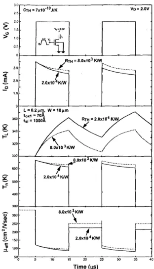
Fig. 2 shows t,he transient perforinance in terms of tirain current, lattice and electron temperatures, arid efiective mobility of a . P D SO1 KMOS device with a channel length of 0.2pnij a channel width of IOprn, a. gate oxide of 70A, and a silicon thin-film of lOOO-&, considering the therma.1 effects: a thernial capacitance of C.r-fr'= 7 x 10-'"J/K arid a thermal resist,a,nce of R.I.I., = 2 x 10⁴K/W am1 from I)\' to 2V with a rise/fa.ll time of 0.111s is imposed (xi
8 x lU3AK/T-II' based 0 1 1 PD-SO1 SPICE result,S. -4 pulse
3 0
.
VD = 2.ov
CTH = 7~10.‘~J/K
-
1 5Time (.s)
Fig. 2: ‘li.ansieiit pc:rhonnant.e of a 0.2/tm P D SO1 NMOS device in terms of drain current: litttice arid clectrori temperatures and ef-
rcctivc mobility, based on I’D-SO1 SPICE results.
the input of the PD SO1 KMOS device, which is biased at 1 . 7 ~ ~ = 2 V . When the ga,te voltage rises from OV to 21’: the drain current rises t o the maxirriuni value. However,
due t o the heat generated by the power consurnption, t,he
1at.t.ice ternperabure hicreases gradually. Duririg t iirIi-ou of the device, the electron temperature decreases slightly. The electron mobility, which is related t o the electron
arid
the latcice temperatures: reacts accordingly. Hence, t.he drain current decays gradually. When \ . i ~ swit,ches from 21: to (I\‘) the device turns off. Therefore! the lattice tem- perature decreases slowly. When the lattice teinpera.ture is not back t o the room temperature, if Vc; turns high again, the peak dra.in current will be lower than the previous peak value. With a larger thermal resistance: the decrease in the draiii current, due t,o t,hermal effect. is 1l1ore iiot,iceable. Due to a longer thermal time coristarit. ( R ~ & ’ ~ ~ ~ ~ ) at a larger R7.1, the tirile for the lattice tempra.ture t o reach thermal equilibriurii is longer..73
i o
0.6 -
0 0.2 0.4 0.6 0.8 1 1.1 1.4 1.6 1.8 2
Fig. 3: (a) L)raiii current jb) body-source voltage characteristics
of a PI.) SO1 NMOS device biased iri the subttirestiold region, with
its body iio& floating: based on the €’L)-SOl SPICE results: and
measured data.
4.Subthreshold Kink
Fig. 3 shows the subthreshold drain current charac- teristics of a PD SO1 NMOS device biased a t various drain voltages and with its body node floating; based on the FD-SO1 SPICE results arid t,he experiinentdly mea- sured datn[6]. As shown in the figure, as predicted by the PD-SO1 SPICE results arid coIifirrried by the experi- rnentdly rrieaured data, when the drain voltage exceeds l.lI’? a larger drain voltagc lea.& t o a steeper subthreshold
slope-the subthreshold l\:ink effect. In the subthreshold kiiik effect region, when the tirain voltage is increasedl its impact ionizat.iori current dso leads t o the accurnulation of holes in the neutral region. Therefore; the body-source voltage is raised arid the threshold voltage of the surface MOS port,ion is lowered and its drain current. increases suckle~ily- its subthreshold slope is steeper as cornpared t o the case without kink effects. As shown in the figure, as verified by the experirnentally inea.sured data, PD-SO1 SPICE predicts the subthreshold kink effects well.
5.Circuit Examples
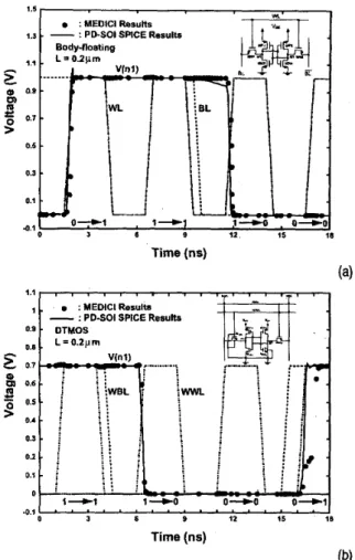
Fig. 4 shows the transient wasefomis of an inverter ciri cuit usirig body-floating PD, body-tied PD aiid DTMOS PD
so1
CIVfOS devices with a channel kn@h of 0 . 3 p i arid a channel width of 10pn; a.t 1’1)~ of 0.7V, based on PD- SO1 SPICE aiid MEDIC1 result,s. As shown in the figure,1
A : MEDIC1 Results
-
: PD-SO1 SPICE Results tax1 644, t o e = 4000HL- 0.3pm, W = 1OFm
Time
(ns)
'Fig. 4: .hintricnt wavel'irnis of' a,u iuvcrter circuit usirig body- floating, body-tied and D'1'hIOS P U SO1 CMOS devices, based cm
I'D-SO1 SPICE, aiid MEDlCI rcsultu.
the DTMOS one has the faster switching speed, follo-ived by the body-floating one. The body-tied t o Vbn/GKD
(for PRIOS/KMOS) one 1ia.s the slowest speed due to body effect.. Fig. 5 shows the write t.ransient waveforms of a 6T SRAhl rneinory cell (a) and a t,wo-port 6T SRAM niem-
ory cell with single-bit-line siinultaiieous read-and-write
access (SBLSRWA) capability (b) 171 using 0.2pm body-
floating(a) arid DTMOS(b) P D SO1 CMOS devices, based on PD-SO1 SPICE and MEDIC1 results. As shown in the figure, as verified by the MEDICI result, the PD-SO1 SPICE results predicts the transients well. Fig.6 s h o w (a.) the write t,ra.risient maveforins of an SRAhl critica.1 path with 42 body-flwting and body-tied P D SO1 CMOS devices and (b) lattice and electron t,empera.tures of the
body-floating P D SO1 KhlOS devices in the SR-khl criti-
cal path, lmseci on PD-SO1 SPICE aiid MEDICI results. -4s shown in the figure, due to the srnaller magnitude in the threshold voltage of the precharge body-floating SO1 NMOS device connect.ed to the hit lines, after precharge, the bit lines (BL) is set at a higher voltage for the hody- floating case. Therefore, a. slower sensing speed can be seen for the body-floating case. As shown, the trend on the elect,rori teriiperat.ures follows the voltage curves ancl the wriation of the lattice temperatures is not noticeable. Via using coinpact BiCIvlOS c:harge-cont.rol eyuivaleiit cir- cuit models, PD-SO1 SPICE yerforriis trarisierit sirnulation of an SR.Ak1 critical path having 42 P D SO1 CMOS cle- vices without coIivergence problems: which are coirirrionly encountered while modeling I'D devices due to kink ef- fects.
1.5
: MEDIC1 Results
1.3
-
-
: PD-SO1 SPICE Results Bod y-bating A L .--- Q) 0.9-
01r"
0.r.
>"
0.5-
1-0 . o - 0 9 11 15 18 0.3-
, 1-1 0.1.
Q.1. 0-l Time (ns) (a)-
: PD-SO1 SPICE Results12 15 111
Time (ns)
(4
Fig. 5: Write transieut waveforms for (a) a 6~ S R ~ W memory cellusing ll.2jmi body-floatiug P D SO1 CMOS devices aud (b) a two-port
GT SILIM niemory cell with single-bit-line simultaneous rc:anl-md- write it(:cxss (SBLSRWA) capability using DTMOS PD SO1 CMOS
dcvices(5). b i L d 011 PI)-SO1 SPICE MIEDICX wsults.
cuit simulation of low-voltage CMOS circuits using deep- subniicrori patially-depleted (PD) SO1 ChiOS devices has been described. Via using BiChlOS charge-control mod-
els, PD-SO1 SPICE performs transient siiriulatioii of the write-access critical path in ai SRAM coinposeti of 42
PD
SO1 CMOS rleyices accurately without convergence prob- ler~is, which are coni~iiorily encountered while nioclelirig F'D devices due to kink effects.Acknowledgments
Conclusion
This work is supported under R.O.C. Kat.ioIial Sci-
111 this paper, I'D-SO1 SPICE: which is lxi,seti on coni- ence Contracts #KSC88-2215-E002-033 ancl #KSC88- pact BiCMOS charge-control riiodels and inclucles seco~id-
order effects, electron a.rid lattice temperat.mes, for cir-
2622-E002-028.
D-
I i\.
Time (ns) r m "
Time (ns)
(b)
Fig. 6: (a.) kVrite transient. waveforms of an StL'IAjI critical path
with 42 body-lloahg and body-lied P D SO1 CMOS devices, based
on I'D-SUI SPICE results. (b) Lattice and electron icniperaturcs of the body-floating P U SO1 N310S devices i n Ihr SHAM critical pa.th: based on PU-SO1 SPICE results.
References
J. €3. Kuo k K. W. SII, "CMOS VLSI Engineering: SilicrJn-on-Insulator (SOI) ," Boston:Kl~uuler, 1998.
M. Canada: C. Akrout, D. Cawthron,
J.
Gout
S. Geissler: R. Houle, P. Kart.schoke, D. Kranier: P. hlcCormick,K.
Rohrer, G. Salern, L. Wa.rriiier,"A
380MHz FUSC Midroprocessor in SOI," ISSCC Dig., pp. 430, 1999.
J . B. Kuo and
J. H.
Lou, "Low-Voltage C!MOSVLSI
Circuits;"New
Yo& Joh,n Wzley, 1999.J .
L. Pelloie,-4.
J. Auberton-Heru, C!. R q ~ i e u d , 0. Faynot, "SO1 'Tedmology Perfomiarice and Mod- elling,': ISSCC Dig.; pp. 428; 1999.J .
I3. Iiiio, K.W.
Su anti S. C. Lin:"Conipa.ct MOS/Bipolai C!liasge-Ciontrol Models of Parfidly- Dep1et.d SO1 T M O S Devices for VLSI CircuitSirriiilatiori-SOI-~~~~liii[)lo~~~ (ST)-SPICE," DZg. of Ewopean Solid-State Denice Research Con!.
(ESS-
DERC), Leuven: Sept.: 1999.[ti] R. Chau; R. Arghavani, Ail. Alavi, D. Douglas, J .
Greason,
R.
Green, S. Tyagi, J . Xu, P. Packan, S. Yu a i d C. Liaiig, "Scalability of Partially Deplet,ed SO1 Techricilogy for Suh-O.25um Logic Applications,';''
IEDM Dig., pp. 591-5'34: 1997.[7] S. C. Liu x i c l J . B. Kuo:"A Novel 0.7V Two-Port. GT SRAhl hleinory Cell Structure with' Single-Bit-Line Sirnultaiieous Read-and-iVrite Access . (SBLSRW-4) Capability using Pastially-I)eplet.ed SO1 I)ynariiic- Threshold Technique," SOI Conf. DZg.: Oct. 1999.
(a)
![Fig. 1 shows t.he compact BiCMOS charge-control mod- els of the P D SO1 NMOS de~ice[5], which are cornposed of the MOS portion at t,he surface a~icl the BJT portion with its base formed by the neutral region and its emit- t.er](https://thumb-ap.123doks.com/thumbv2/9libinfo/8776892.214175/1.918.455.796.247.525/compact-bicmos-control-cornposed-portion-surface-portion-neutral.webp)