行政院國家科學委員會專題研究計畫 成果報告
總計畫(3/3)
計畫類別: 整合型計畫 計畫編號: NSC92-2120-E-009-001- 執行期間: 92 年 08 月 01 日至 93 年 07 月 31 日 執行單位: 國立交通大學電子工程學系暨電子研究所 計畫主持人: 李建平 共同主持人: 孫允武,孫建文 報告類型: 完整報告 處理方式: 本計畫可公開查詢中 華 民 國 93 年 12 月 31 日
行政院國家科學委員會補助專題研究計畫期末報告
※※※※※※※※※※※※※※※※※※※※※※※※
※ 半導體量子結構與量子元件前瞻性研究─ ※
※
子計畫一:半導體量子結構的成長,物理與元件應用
※
※
子計畫二:量子結構之光學特性及量子點雷射之載子及
※
※
增益動態研究
※
※
子計畫三:奈米量子元件製作及高頻與磁傳輸特性
※
※※※※※※※※※※※※※※※※※※※※※※※※
計畫類別: 整合型
計畫編號:NSC92-2120-E-009-001
執行期間:92 年 08 月 01 日至 93 年 7 月 31 日
總計畫主持人:李建平
子計畫(一)主持人:李建平
子計畫(二)主持人:孫建文
子計畫(三)主持人:孫允武
執行單位:國立交通大學 電子工程系
中 華 民 國九十三年 十二 月 二十八 日行政院國家科學委員會專題研究計畫期末報告
半導體量子結構與量子元件前瞻性研究
Semiconductor Quantum Structures and Quantum Devices
計畫編號:NSC92-2120-E-009-001
執行期限:92 年 8 月 1 日至 93 年 7 月 31 日
總主持人:李建平 國立交通大學電子工程系
中文摘要 此報告為總結本實驗室在本年度 於「半導體量子結構與量子元件前瞻 性研究」專題計畫的研究成果。利用 分 子 束 磊 晶 系 統 ( Molecular Beam Epitaxy System; MBE),我們設計一系 列之實驗來驗證量子環形成機制。此 外,我們也探討利用砷化銦在砷化銦 鎵上成長量子線物理特性在雷射上的 行為。 我們也利用自製的高靈敏度微波 向量偵測系統研究量子線陣列的高頻 動態磁傳輸特性,發現邊緣磁電漿受 激態到量子霍爾態的轉換。我們也利 用高頻的表面聲波研究量子線陣列。 在其中的一個子計畫中我們研究 了 量 子 井 及 量 子 點 中 載 子 的 動 態 過 程。我們也於 SiGe 量子點中發現到不 尋常的可見光螢光。利用電子數微影 技術我們成功製造出次波長光柵於半 導體基板上。 關鍵詞:砷化鎵、砷化銦、砷化銦鎵、 量子線、量子環、分子束磊晶。 I. AbstractThis reports summarized the results of joint research project “Semiconductor quantum structures and quantum devices” in this year. Using molecular beam epitaxy (MBE) system, a series of experiments with different GaAs capping or annealing process was designed to verify the formation mechanism of InGaAs quantum rings. In addition, we have also studied the laser behavior by utilization of InAs quantum wire (QWrs) on InGaAs.
We have studied the dynamics magnetotransport properties of quantum-wire arrays with our homemade high-sensitivity microwave vector detection system, and mapped out
magnetoplasma and quantum Hall states. We have also studied the surface acoustic wave adsorption of quantum-wire arrays.
In one of the sub-project, we have investigated the carrier dynamics in semiconductor QWs and QDs. We also
uncover unusual visible photoluminescence from assembled SiGe quantum dots. A sub-wavelength grating was also demonstrated via e-beam lithography.
Keywords: GaAs, InAs, InGaAs,
quantum wire, quantum ring, molecular beam epitaxy.
II. Results and Discussion
(A) growth of nanostructures and devices
Varian GEN Ⅱ MBE system was used to grow InAs quantum dots on (100) GaAs substrate. Then, various growth processes are used to form quantum rings. We used various GaAs capping and annealing conditions to control the In-Ga intermixing and diffusion length of In adatoms on the surface. With controlling (or altering) the diffusion-related processes, we could study and verify the formation mechanism of QDs for clarity. The detailed growth conditions are listed in Table 2
The AFM images in Fig.1 show the surface morphology of quantum rings with different growth conditions. Crater-like nanoholes are found on all samples.
(Ia) (IIa)
(Ib) (IIb)
(Ic) (IIc)
Fig.1. The surface morphology of quantum rings
with different growth conditions.
There are three significant features exhibited in the surface morphology: First, crater-like nanoholes (as shown in Fig. 1(Ib)) were formed even though the capped QDs were cooled down immediately without annealing. However, there is no depression in the center for the uncapped QDs. Secondly, the diameters of the nanoholes are strongly dependent on the capping / annealing conditions. The last feature is that there exist binomial size distributions of inner holes in sample IIb. We attribute this to significant In-Ga intermixing (In(Ga)As alloy) taking place during slow capped GaAs process (0.3µm/hr).
We can give a simple conclusion as follows: Quantum rings formation is a two-step process. The initial process for depression in the center is originated from an unbalanced outward force caused by wetting droplet instability. However, the temperature and the time of annealing, as well as the alloying effect during capped GaAs strongly influence the migration behavior of out-diffusive In atoms, leading to a variety of surface morphology
We also investigated the property of the InAs QWrs laer. The InAs QWrs was grown on the InGaAs lattice match to InP. The di rect ion of th e QWrs is alon g [110]. For comparison of the polarization behavior, two kinds of laser contact stripes with different direction were made : One with the contact stripes aligned to[110], and another with the contact stripes aligned to[110].
The lasing spectra and the L-I curve were recorded under different temperature. The Ith v.s. temperature of
the LD along [110] and [110] direction were shown in Table.2 respectively. Fig.2 was the lasing wavelength just above threshold current along [110] and [110] direction.
Temp Ith// (mA)
Ith+
(mA) Ith// : Ith+ 20K 48.89 2.29 21.35 40K 59.07 2.76 21.4 60K 62.11 3.82 16.26 80K 85.89 4.58 18.75 120K 115.96 8.88 13.06 140K 139.36 13.22 10.54 160K 188.53 42.2 4.47 180K 271.7 90.64 3
Table.1: The Ith v.s. temperature of the
LD along [110] and [110] direction
From the Comparison with the lasing spectra of the LD and the PL, the LD with cavity direction along [110] was
ground state lasing, but the LD with cavity direction along [110] was excited
state lasing. This was due to HH and LH band structure mixing in the QWrs. After the HH and LH band structure mixing in the QWrs, light emission probability for polarization parallel QWrs would be larger than perpendicular QWrs. As a result, LD with cavity direction along [110], which
the light polarization was parallel to QWrs, was much easier to laser in the ground state than LD with cavity direction along [110], which the light
polarization was perpendicular to QWrs.
1500 1550 1600 1650 1700 1750 1800 1850 0.0 0.2 0.4 0.6 0.8 1.0 1.2 1.4 1.6 1704 In te n s it y ( a rb .) w avelength (nm ) PL @ 100K 0.4 0.6 0.8 1.0 1.2 1.4 1723.5576 9 In te n s it y ( a rb .)
Lasing sp ectrum of Q W r LD + w ire @ 1 00K I=50m A ; Ith=6.36m A
(B) Carrier dynamics in quantum wells at the presence of cold Fermi seas
We investigate experimentally the scattering mechanisms between the electrons and holes and the influence of an electron and hole distribution near k=0 on the femtosecond carrier thermalization process in modulation doped GaAs/AlGaAs quantum wells. In contrast to the earlier report by Knox et al., we find that the presence of a cool thernalized distribution at zone center does not affect the scattering rate significant. We have compares the scattering rate of hot electron in the undoped and n-modulation doped QW samples. The rate that carriers form a thermalized distribution is determined from the rise time of the photoluminescence. In the undoped wells, luminescence intensity rise time is on the order of 500 fsec at an excitation
density of 1x1011 cm-2. We also find that the pre-existing carrier population does not speed up the carrier-carrier scattering significantly. When a nonthermal distribution is immersed in a dense Fermi sea, the rate that populates the bandedge states has slow down due to the band filling effect. The calculated scattering for photoexcited carriers in the presence of a cool distribution does not occur on a time-scale much less than 100 fsec.
(C)Visible photoluminescence from Ge/Si quantum dots
Spectroscopic analyses on stacked Ge quantum dots on Si(100) substrates are carried out. For the first time, strong visible light photoluminescence around 620 nm from stacked Ge quantum dots is observed. The luminescence is stable and clearly visible to the naked eye at both room temperature and low temperature. We have investigated the temperature dependence of the luminescence, as well as the composition of Ge dots via transmission electron miscroscopy and the Raman spectroscopy. Possible cause of the visible luminescence is attributed to the L-to-X crossover in the conduction band minimum due to the quantum confinement.
(D) Subwavelength grating fabricated on GaAs substrates via e-beam lithography
We have demonstrated the design and fabrication of polarizing mirror/absorber based on a 1500 1550 1600 1650 1700 1750 1800 1850 0.0 0.1 0.2 0.3 0.4 0.5 0.6 0.7 0.8 0.9 1.0 1.1 1571.15385 1590.38461 In ten s it y (ar b .) w avelength (nm )
Lasing spectrum of Q W r LD // w ire @ 100k I=170m A ; Ith=102.39m A
Fig.2 (a)PL spectrum at 100K. (b)Lasing spectrum at 100K with contact strip perpendicular to QWrs. (c) Lasing spectrum at 100K with contact strip parallel to QWrs.
subwavelength metal grating on GaAs (100) wafer via electron beam lithography and lift-off method. This device can reflect light polarized perpendicular to the grating grooves and absorb light polarized along the grating grooves. This device operates as a polarizing mirror or absorber at normal incidence for a semiconductor laser diode emitting at a wavelength of 650 nm. Such a compact device could be easily integrated with semiconductor based light emitting devices or replace bulky and costly birefringent crystal prisms.
(E)Carrier capture in InAs/GaAs QDs
We have investigated the carrier capture and relaxation processes in InAs/GaAs self-assembled quantum dots at room temperature by time-resolved photoluminescence techniques with a high time resolution of ~ 150 fsec. Following the initial fast relaxation in GaAs barriers, we have observed rising processes in time-resolved PL intensity at the energies of quantum dot confined states and the wetting layer. The rising processes are assigned to the carrier capture from the barriers into the wetting layer and confined states in InAs dots and subsequent relaxation in each detected energy level. We found that the carrier capture rate is faster than the intra-dot relaxation within the range of excitation densities that we investigated. Under high excitation intensity, the electronic states in the dots were
captured from the barrier. However, at low excitation densities, the PL rise times were influenced by the carrier diffusion.
(F) Very-high-sensitivity PLL vector receiver at very low microwave power
We have developed a microwave receiver using phase-lock-loop technique, which can be used to detect the properties of electrons in quantum structures, such as quantum dots (QDs) or quantum wires (QWs), at low temperatures (below 1K). The frequency range is from 100MHz up to 18GHz. The advantages of our homemade receiver compared to commercial vector network analyzers (VNAs) are the following:
(1) We can detect a phase change smaller than 0.001° while the average input power at the sample is below –100dBm.
(2) We can detect an amplitude variation below 0.1% at the same time. That is to say the amplitude resolution is better than 0.0087dB at very low power levels described above.
Combining this powerful high-sensitivity and low-power microwave detecting system with our existing cryogenic systems (a He3 fridge with a base temperature of 0.3K and a dilution fridge with a base temperature of 30mK) and superconducting magnet, we have set up a very unique facility for
dimensional electron systems (LDESs) at microwave frequencies. The preliminary result has been published in Applied Physics Letters 85, 4196 (2004).
(G)Detecting the properties of LDESs with PLL vector receiver and coplanar waveguide (CPW) sensors
We are the first one in the world to use a PLL vector receiver to measure the microwave transport properties of LDESs imbedded in the gap of CPWs.. The edge magnetoplasma, a collective excitation around the edge of the sample, and the field dependence has been predicted theoretically for mesoscopic electronic system with sample dimension smaller than the characteristic width of the edge channel in strong magnetic fields. However, clear experimental results for quantum wire system are still in deficiency. Our results clearly confirm the theoretic prediction. Besides that, we also measured the change of the dielectric constant, or the electric polarization, of the quantum wire system in the condition that the edge magnetoplasmon was observed. We are preparing manuscript for this result for the Rapid Communication in Physical
Review B.
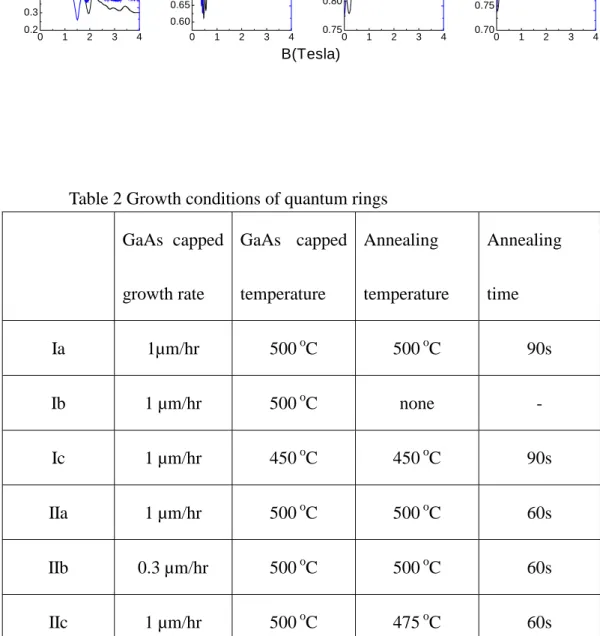
(H) Magnetotranport properties of quantum wire arrays probed by SAW
In this study, we put a quantum wire array (6000x1umx20um) between
two SAW IDTs and measure the amplitude and phase change while sweeping B. The schematic of the sample structure is shown in Fig. 3. The experimental results are shown in Fig. 4 for fundamental frequency and odd harmonics up to order 7. Anomalous adsorption and phase shift are observed at low harmonics while the data become SdH-like at high frequencies. We have performed similar experiment for samples of a different wire orientation, and obtained different behavior.
Figure 4 Amplitude and phase shift of the transmitted SAW signals through a quantum wire array at different harmonics.
Table 2 Growth conditions of quantum rings
GaAs capped growth rate GaAs capped temperature Annealing temperature Annealing time Ia 1µm/hr 500 oC 500 oC 90s Ib 1 µm/hr 500 oC none - Ic 1 µm/hr 450 oC 450 oC 90s IIa 1 µm/hr 500 oC 500 oC 60s IIb 0.3 µm/hr 500 oC 500 oC 60s IIc 1 µm/hr 500 oC 475 oC 60s 0 1 2 3 4 0.2 0.3 0.4 0.5 0.6 0.7 0.8 0.9 1.0 1.1 ∆ A (%) f0=556MHz 0 1 2 3 4 0.60 0.65 0.70 0.75 0.80 0.85 0.90 0.95 1.00 1.05 f0=1.6GHz 0 1 2 3 4 0.75 0.80 0.85 0.90 0.95 1.00 B(Tesla) f0=2.7GHz 0 1 2 3 4 0.70 0.75 0.80 0.85 0.90 0.95 1.00 f0=3.8GHz ∆ f / f0 (a rb . u n it)