行政院國家科學委員會專題研究計畫 成果報告
子計畫三:先進無線通訊系統之關鍵射頻積體電路(I)
計畫類別: 整合型計畫 計畫編號: NSC93-2219-E-009-026- 執行期間: 93 年 08 月 01 日至 94 年 07 月 31 日 執行單位: 國立交通大學電信工程學系(所) 計畫主持人: 孟慶宗 計畫參與人員: 吳宗翰 吳澤宏 報告類型: 完整報告 報告附件: 出席國際會議研究心得報告及發表論文 處理方式: 本計畫可公開查詢中 華 民 國 94 年 8 月 22 日
行政院國家科學委員會補助專題研究計畫
■ 成 果 報 告
□期中進度報告
先進無線通訊系統之關鍵射頻積體電路
(2/3)
Key RFICs for advanced wireless communication system
計畫類別:□ 個別型計畫 ■ 整合型計畫
計畫編號:NSC93-2219-E-009-026-
執行期間:
93 年 8 月 1 日至 94 年 7 月 31 日
計畫主持人:孟慶宗 國立交通大學電信系
計畫參與人員:吳宗翰 吳澤宏 國立交通大學電信系
成果報告類型(依經費核定清單規定繳交):■精簡報告 □完整報告
本成果報告包括以下應繳交之附件:
□赴國外出差或研習心得報告一份
□赴大陸地區出差或研習心得報告一份
■出席國際學術會議心得報告及發表之論文各一份
□國際合作研究計畫國外研究報告書一份
處理方式:除產學合作研究計畫、提升產業技術及人才培育研究計畫、
列管計畫及下列情形者外,得立即公開查詢
□涉及專利或其他智慧財產權,□一年□二年後可公開查詢
執行單位:國立交通大學電信系
中 華 民 國 94 年 7 月 31 日
行政院國家科學委員會專題研究計劃期末報告
先進無線通訊系統之關鍵射頻積體電路
(2/3)
Key RFICs for advanced wireless communication system
計畫編號:NSC 93-2219-E-009-026 執行期限:93 年 8 月 1 日至 94 年 7 月 31 日 主持人:孟慶宗 國立交通大學電信系 計畫參與人員: 吳宗翰 吳澤宏 國立交通大學電信系 一、中文摘要
本計劃利用0.35um SiGe BiCMOS 製程實現了一個利用LC電流合成器產 生單端輸出之5.7GHz升頻微混頻器, 混頻器擁有-4dB的轉換增益;一個具 鏡像訊號抑制的5.2GHz雙正交四相位 降頻器,降頻器擁有1dB的轉換增益與 具有47dB的鏡像訊號抑制能力;一個 整合集總元件Rat-Race與LC電流合成 器的5.2GHz升頻微混頻器。實驗結果 與模擬結果大致符合,實驗結果顯示 混頻器擁有-1dB的轉換增益。 二、計畫緣由與目的 一般來說,SiGe BJT(鍺化矽雙 極性電晶體)技術由於他的截止頻率 高且有較好的特性表現,因此通常被 用來實現射頻前端電路。單晶射頻積 體電路(RFIC)在提供小面積、高重製 性、高穩定性及在大量生產時的低價 格 方 面 , 給 射 頻 技 術 一 個 很 好 的 選 擇。而砷化鎵晶片雖然價格較高,但 在材料的本質上仍勝過矽一大步。但 隨著SiGe 製程技術快速的進步,用此 技術來實現前級電路是很方便的,因 此將會使得更多人享受行動通訊及無 線網路之便利。現在我們在實際應用 上已經有以下幾個頻段的需要:GSM (900MHz&1800MHz) , GPS(1600Mhz) , DECT(1900Mhz) , DBS(950-2150MHz)等等,都需要放大 器的應用。更重要的是由於無線區域 網路(Wireless LAN)的興起,使得在 2.4GHz、5.2GHz (汎歐規)及 5.7GHz 的頻段出現了應用。因此我們特別選 擇這些頻段作為研究重點。 三.研究成果與方法 我們利用了SiGe製程技術,來實 現了一個可以在5.7GHz操作之吉伯特 升頻微混頻器。我們採用一個被動電 感電容合成器使微混頻器的差動輸出 轉為單端輸出,同時加倍輸出電流。 而微混頻器在本質上就具有寬頻的單 端輸入阻抗匹配,因此一個具有單端 輸入與單端輸出的吉伯升頻混頻器之 運作可以達成。LC電流合成升頻器的 電 路 圖 為 圖 一 。 我 們 這 裡 採 用RF
Micro Mixer Cell架構,來轉換不平衡 的信號為平衡的信號,同時利用高速 的BJT來提高工作頻寬及轉換增益。其 他的部分再利用LC電流合成的電路, 使雙端輸出轉換成單端輸出。一般我 們通常會使用主動Balun 作為雙端轉 單端電路,不過主動Balun 本身常受到 電 晶 體 速 度 的 限 制 , 且 線 性 度 也 較 差。因此我們這個升頻器的RF 輸出端 採用LC電流合成的方式將差動輸出訊 號轉換成單端輸出。 我們從圖二來看一次LC電流合成 器的原理推演。我們將寄生電阻加入 後,利用戴維寧與諾頓轉換,將電路 2
作電流源與電壓源轉換,當電路操作 在共振頻率時,串聯的電感與電容會 近似短路,而並聯的電感與電容會近 似開路,化簡為圖二(d),在其中定義Q 值之後代入Io',發現當電感Q值夠大 時,Io'會等於-Io,而串聯的Cs和Rs與 串聯的Ls和Rs則可以利用與Q值之間 的關係,化為並聯的Rp、Cp與Lp、Rp, 在共振頻率時Cp與Lp又化為開路,所 以最後就剩下兩個並聯的Rp與兩倍的 Io。因此我們知道要有好的轉換增益, 就必須要有高的Rp,要有高的Rp就要 有高Q值的電感,但這也是困難的地 方。 在複數降頻器電路設計上,為了 達到更高的鏡像抑制功能,我們使用 雙正交的複數降頻器,由於RF訊號先 經過正交的路徑大大減少了中頻鏡像 訊號造成的重疊,使得提高了鏡像抑 制的能力。雙正交相位複數降頻器電 路圖的電路圖為圖三。包含了四個混 頻器所組成的雙正交複數降頻器、去 除鏡像訊號的RC-CR多相位濾波器、 LO及RF的正交相位產生器,以及RF 輸入端的被動差動訊號產生器。由於 RF訊號先經過正交的路徑大大減少了 中頻鏡像訊號造成的重疊,使得提高 了鏡像抑制的能力。在圖四(a)中利用 重疊原理,可以看出相位為0º 的輸入 訊號在等效上看到一個CR高通濾波 器,而相位為90º 的輸入訊號等效上看 到一個RC低通濾波器。在極點頻率 時,其相位分別落後45º(+45º)及超前 45º (-45º)。因而相位為0º的輸入訊號落 後45º成為45º,而相位為90º的輸入訊 號超前45º成為45º,即輸出的訊號同 相。而在圖四(b)中利用相同的重疊原 理,分別輸入0º、270º 的訊號,因而 相位為0º的輸入訊號落後為45º,但相 位 為270º 的 輸 入 訊 號 超 前 45º 成 為 225º,因而輸出的訊號相差180º,此時 無訊號輸出。由以上我們可得知,對 於一個逆時間方向的正頻率訊號可以 順利到達輸出端,而對於一個逆時間 方向的負頻率訊號則在到達輸出端前 被相減。由於LO輸入部份需要I/Q的訊 號,因而我們一樣可以利用RC-CR的 多相位濾波器來產生。如圖五所示, 一差動的訊號等效上可以看成正頻率 與負頻率的組合,由於多相位濾波器 可以分辨正負頻率的差別,因此一差 動訊號可經由多相位濾波器濾除負頻 率項後產生所需的正交訊號。我們這 裡使用吉伯特混頻器,如圖六。再加 上共集極電晶體以防止後面的多相位 濾波器所造成的負載效應。最後再使 用一個簡單的差動放大器來當作中頻 輸出級,如圖七,將中頻信號合成以 方便量測。 而整合集總元件Rat-Race與LC電 流 合 成 器 的 升 頻 微 混 頻 器 電 路 如 圖 八,本電路大部分的架構都與前一個 LC電流合成器相似,但是我們修改了 RF輸入級為更平衡的結構,同時將產 生LO差動訊號所需的Rat-race以集總 元件的方式時限內建在晶片裡,並且 修改輸出級由原先的LC低通濾波器換 為CC-CC輸出級。如圖八,LO 信號連 接到一個集總元件組成的Rat-race。因 為在RF的量測環境中,通常有很多用 來 連 接 探 針 與 儀 器 的 訊 號 線 與 轉 接 器,而這些外部的連接多是造成輸入 訊號不平衡的原因。而現在的製程技 術已微小到可以在這樣的高頻下,讓 集總Rat-race整合到晶片中,所以最直 接的作法便是將Rat-race作進晶片裡。 集總元件Rat-race 電路如圖九所示。在 此升頻器的輸出部份,一樣使用電流 合成器輸出單端電流,為了使電流合 成器不受外部的電路影響,在輸出端 加上一個CC-CC的緩衝級隔離外部的 電路,如圖十所示。 我們可以發現輸出電壓緩衝級實 際 上 是 提 供 功 率 增 益 。 更 進 一 步 地 說,由電壓緩衝級得到的功率增益要 比我們在前一個電路裡所採用的純電 抗匹配來的好。LC電流合成器電路的 等效單端輸出電路如圖十一所示,將 3
諾頓等效電路轉換為戴維寧等效電路 是為了討論傳遞到負載的功率。如圖 十一(b),如果使用一個電抗匹配網路 來匹配LC電流合成器輸出阻抗至50歐 姆,最大傳遞到負載的功率同時達到 共軛狀態時,可以用下式來表示: 2 L Passive Matching 4 sig sig I R P = 而 如 果 使 用 的 是 主 動 輸 出 電 壓 緩 衝 級,我們可由圖十一(c)來說明。電壓 緩衝級的輸出阻抗為50歐姆,而輸入 阻抗則遠大於LC電流合成器的阻抗, 所以當使用主動輸出電壓緩衝級時, 傳遞到負載的功率可以表示為: 2 2 2 L Active Buffer 0 0 4 4
sig sig sig
V I R P Z Z = = i 比較兩式,使用主動輸出級之傳遞到 負載的功率較高。因此,功率提升度 可以由兩式的比值來表示: 2 2 L Active Buffer 0 2 L Passive Matching 0 0 4 2 4 sig sig sig P sig sig I R R P Z R P = I R = Z = Z i i 在類比電路設計中,輸出緩衝級 不提供電壓增益,然而共集極輸出緩 衝級能提供功率增益。事實上,功率 增益是由主動輸出緩衝級而來,而主 動輸出緩衝級藉由電流信號來提供額 外的功率而不是藉由電壓信號。值得 注意的是主動輸出緩衝級的輸入阻抗 與電流合成器的輸出阻抗並非互相共 軛。這個設計方法與微波放大器電路 的電抗匹配原理相當不同。這裡的設 計概念不只符合類比電路設計概念, 也同時讓我們清楚知道由類比IC設計 裡的電壓電流增益,轉換到RFIC設計 裡的功率增益。 四.結果與討論 圖十二為LC電流合成升頻器電路 晶片照片。而圖十三顯示LC電流合成 升頻器轉換增益對LO power的量測圖 形。當LO power為3dBm時,轉換增益 峰 值 約 為-4dBm 。 當 LO power 從 -10dBm增加到3dBm時,轉換增益隨之 由-6dB增加到-4dB。換句話說,混頻 器核心只需要低功率的本地震盪源, 並且對理想的轉換增益具有寬的LO power範圍。圖十四顯示RF輸出反射損 耗在5.7GHz時約為-25dB。RF輸出阻抗 匹配我們是利用一個LC低通濾波器來 作的。在我們的電路設計裡,操作頻 率為5.7GHz而量測結果顯示出輸出反 射 損 耗 正 好 在5.7GHz的位置有個凹 口,顯示我們的阻抗匹配作得很好。 圖十五可以得知這個LC電流合成器的 功 率 特 性 表 現 。 實 驗 的 數 據 顯 示 OP1dB為-9.5dBm,OIP3為-1.5dBm, 因此我們可以知道這個架構的線性度 很不錯。 圖十六為雙正交相位複數降頻器 晶片照片。我們從量測結果圖十七可 以 發 現 , 當 降 頻 混 頻 器 的 RF=5.2GHz、LO=5.17GHz,LO power 為0dBm時,電路具有1dB的轉換增 益。從圖中可以發現,當LO power從 0dBm增加到10dBm時,轉換增益仍維 持在1dB左右。換句話說,混頻器所需 要的LO power不大,同時具備寬的LO power變化範圍來達成我們所要求的 轉換增益。因此我們的吉伯特混頻器 核心具有低LO power與寬LO power變 化範圍的兩個優點。由圖十八中可以 看到在15MHz到45MHz的IF頻段,IRR 大於47dB。 圖十九為整合集總元件Rat-Race 與LC電流合成升頻器電路晶片照片。 圖二十顯示轉換增益對LO power的量 測圖形。當LO power為0dBm時,轉換 增益峰值約為-1dBm。當LO power從 -6dBm增加到5dBm時,轉換增益維持 在-1dB。圖二十一為電路的IF埠與RF 埠 反 射 損 耗 。RF 輸 出 反 射 損 耗 從 0.1GHz 一 直 到 20GHz 都 在 -13.5dB 以 下。微混頻器具有寬的輸入阻抗匹配 頻寬,所以在圖中可以看到從低頻一 4
直到20GHz,IF的輸入阻抗匹配約在 -10dB以下。圖二十二可以得知這個LC 電流合成器的功率特性表現。實驗的 數 據 顯 示OP1dB 為 -10dBm , OIP3 為 6dBm,因此我們可以知道這個架構的 線性度非常不錯,而這個電路的高線 性度應該是直接來自因使用了被動電 感 電 容 電 流 合 成 器 來 當 作 負 載 的 緣 故。 五.計畫成果與自評 研究內容和原計畫完全相符,達 成了預期目標情況,已發表在相關學 術期刊及研討會中。 六.參考文獻
[1] B. Gilbert, “The MICROMIXER: A highly linear variant of the Gilbert mixer using a bisymmetric Class-AB input stage,” IEEE J. Solid-State Circuits, Vol. 32, pp. 1412-1423, Sept. 1997.
[2] J. Durec and E. Main, “A linear class AB single-ended to differential transconverter suitable for RF circuits,” IEEE MTT-S Dig., pp. 1071-1074, 1996. [3] C. C. Meng, S. K. Hsu, A. S. Peng, S. Y. Wen and G. W. Huang, “A fully integrated 5.2 GHz GaInP/GaAs HBT upconversion micromixer with output LC current combiner and oscillator”, IEEE MTT-S international microwave symposium. pp. A205-A208, 2003. [4] C. C. Meng, S. S. Lu, M. H. Chiang, and H. C. Chen, “DC to 8 GHz 11 dB gain Gilbert micromixer using GaInP/GaAs HBT technology”, Electronics Letters, pp.637-638, April 2003.
[5] C. C. Meng, S. K. Xu, T. H. Wu, M. H. Chao and G. W. Huang, “A high isolation CMFB downconversion micromixer using 0.18 um deep n-well CMOS technology”, IEEE MTT-S international microwave symposium. pp. A105-A108, 2003.
[6] F. Behbahani, Y. Kishigami, J. Leete, and A. Abidi, “CMOS Mixers and Polyphase Filters for Large Image Rejection,” IEEE Journal of solid-state circuits, VOL. 36, NO. 6, JUNE 2001.
[7] J. Crols and M. Steyaert, “Fully Integrated 900 MHz CMOS Double Quadrature Downconverter,” Proc. ISSCC, Session 8.1, San Francisco, Feb. 1995.
[8] J. Crols and M. Steyaert, “A Single-Chip 900 MHz CMOS Receiver Front-End with a High Performance Low-IF Topology,” IEEE J. of Solid-State Circuits, vol. 30, no. 12, pp. 1483-1492, Dec. 1995.
[9] M. Steyaert, M. Borremans, J. Janssens, B. D. Muer, N. Itoh, J. Craninckx, J. Crols, E. Morifuji, H. S. Momose and W. Sansen, “A single-chip CMOS transceiver for DCS-1800 wireless communications” Proc. ISSCC, San Francisco, Feb. 1998.
Vin_IF Q3 Q7 Q6 Q5 Q4 Q2 Q1 r1 r2 C1 L1 L2 Lm Cm Vout LO + LO -Q8 Q9 r3 r4 r5 圖一 LC 電流合成升頻器電路 I0 I0 RS RS CS LS LS V0 I0 RS RS CS LS R S S 1 ω = L C I0 RP RP R S S R S S ω L 1 Q = = R ω C R I0 RS RS CS LS ′ R S S R S S 0 0 0 R S S S R S 0 0 jω L +R jω L + R I =I ( )= I ( ) 1 + R -jω L + R jω C jQ + 1 =I (- ) -I jQ -1 (a) (b ) (c) (d ) (e) (f) I0 RS RS CS LS LSCS 2 P S R =R (1 +Q ) 2 P S 2 Q + 1 L =L ( ) Q 2 P S 2 1 +Q C =C 0 0 R S S V =I (jω L +R ) V =I (jω L +R )0 0 R S S V0 LP CP Q 2 +- +-Isig Rsig ′ I′0 0 I I if Q >>1 ≈ sig 0 jQ +1 0 I =I ( +1 ) 2I jQ -1 P sig R R = 2 圖二 加入寄生電阻之電流合成器等 效轉換圖 5
LO+ LO-RF+ RF- IF-I+ I-Q+ Q-I+ I-Q+ Q-II+
IQ-IQ+ II- QI-QQ- QI+QQ+
Vdd IF+ 圖三 雙正交相位複數降頻器電路圖 0 V∠ 90 V∠ 180 V∠ 270 V∠ '0 45 V∠ + '90 45 V∠ − ⇒2V'∠45 1 2 3 4 0 1 . input freq RC ω = = R R C R R C C C 0 V∠ 90 V∠ 180 V∠ 270 V∠ VV'∠'∠ +270 450 45− ⇒0 1 2 3 4 0 1 . input freq RC ω = = R R C R R C C C (a) (b) 圖四 RC-CR 多相位濾波器(a)正頻率 (b)負頻率選擇 0 0 0 180 0 180 0 0 0 90 0 270 1 2 3 4 1 1 2 2 3 3 4 4 + ⇒ 圖五 正交訊號產生器 R3 R5 R2 Q1 Q2 Q3 Q4 Q5 Q8 LO2+ LO2-Vdd R1 R4 Q6 Q10 Q9 Q7 R6 R7 圖六 吉伯特混頻器 R3 R5 R2 Q1 Q2 Q4 Vdd R1 R4 Q3 Q5 Q6 R6 R7 圖七 中頻輸出級 LO Input IF Input LC Current Combiner RF Output Q1 Q2 Q4 Q5 Q6 Q7 Q3 Q8 Q9 Q10 Q11 Q12 Q13 Q14 R1 R2 R3 R4 R5 R6 R7 R8 L1 C1L2 L3 L4 L5 L6 C2 C3 C4 C5 C6 C7 C8 50 VCC Lumped Rat-Race LO Input Stage 圖八 內建集總 Rat-race 之 LC 電流合 成升頻器電路 6
2C C 2C C L L L L C C Port 1 Port 2 Port 3 Port 4 C C L (a) (c) C L C (b) Port 2 3λ/4 λ/4 λ /4 λ/4 Zo Zo Zo Zo 2Zo Port 1 Port 3 Port 4 圖九 集總 Rat-Race Vcc IN OUT 圖十 CC-CC 輸出級 Z0 Z0 Z0 Z0 Lossless Passive Output Matching Network (a) (b) (c) Isig Z0 Rsig Z0 V Rsig sig Vsig Rsig Z0 Rout Vsig Rsig Active Output Buffer Rout Z0 Vsig Rout>>Rsig 圖十一 LC 電流合成級與射頻輸出級 的輸出功率轉換 圖十二 LC 電流合成升頻器晶片照片 -20 -15 -10 -5 0 5 10 -16 -14 -12 -10 -8 -6 -4 -2 0 2 Co nve rs ion Gai n ( d B) LO Power (dBm) LO Frequency=4.9GHz IF Frequency=300MHz 圖十三 LC 電流合成升頻器電路轉換 增益對LO 功率量測結果 0 1 2 3 4 5 6 7 8 9 10 11 12 13 14 15 16 17 18 19 20 -35 -30 -25 -20 -15 -10 -5 0 S22 S22 (dB ) Frequency (GHz) 圖十四 LC 電流合成升頻器電路 S22 量測結果 7
-25 -20 -15 -10 -5 0 5 10 15 20 -120 -110 -100 -90 -80 -70 -60 -50 -40 -30 -20 -10 0 10 20 LO Power=4dBm LO Frequency=5.4GHz IF Frequency=300MHz Pout (f1) Pout (2f1-f2) Out p u t Po w er ( d B) Input Power (dBm) OP1dB=-9.5 dBm OIP3=-1.5 dBm 圖十五 LC 電流合成升頻器電路功率 特性量測結果 圖十六 雙正交相位複數降頻器晶片 照片 -20 -15 -10 -5 0 5 10 -15 -10 -5 0 5 C o n versi on G ai n ( d B) LO Power (dBm) RF Frequency=5.2GHz LO Frequency=5.17GHz IF Frequency=30MHz 圖十七 雙正交相位複數降頻器電路 轉換增益對LO 功率量測結果 0 10 20 30 40 50 60 70 80 90 100 10 20 30 40 50 60 Im ag e R ejec tio n (d B ) IF Frequency (MHz) LO Frequency=5.17GHz 圖十八 雙正交相位複數降頻器電路 IRR 量測結果 圖十九 內建集總 Rat-race 之 LC 電流 合成升頻器晶片照片 -20 -15 -10 -5 0 5 10 -16 -14 -12 -10 -8 -6 -4 -2 0 2 Co nversion G ain ( d B) LO Power (dBm) LO Frequency=4.9GHz IF Frequency=300MHz 圖二十 內建集總 Rat-race 之 LC 電流 合成升頻器電路轉換增益對LO 功率 量測結果 8
0 2 4 6 8 10 12 14 16 18 20 -30 -25 -20 -15 -10 -5 0
IF Input Return Loss(dB) RF Output Return Loss(dB)
Re turn Lo ss (d B) Frequency (GHz) 圖二十一 內建集總 Rat-race 之 LC 電 流合成升頻器電路S 參數量測結果 -35 -30 -25 -20 -15 -10 -5 0 5 10 15 -100 -90 -80 -70 -60 -50 -40 -30 -20 -10 0 10 20 LO Power=0dBm LO Frequency=4.9GHz IF Frequency=300MHz Pout (f1) Pout (2f1-f2) O u tput Po w er (dB) Input Power (dBm) OP1dB=-10dBm OIP3=6dBm 圖二十二 內建集總 Rat-race 之 LC 電 流合成升頻器電路功率特性量測結果 9
發表之論文
Tzung-Han Wu, Chinchun Meng, Tse-Hung Wu and Guo-Wei Huang “A 5.7 GHz 0.35 um SiGe HBT Upconversion Micromixer with a Matched Single-ended Passive Current Combiner Output”, European Microwave Conference - European gallium arsenide and other semiconductors application symposium (GAAS 2004), Amsterdam, Netherlands, October 11-15, 2004, pp.323~326
Tzung-Han Wu, Chinchun Meng, Tse-Hung Wu and Guo-Wei Huang, “A Fully Integrated 5.2 GHz SiGe HBT Upconversion Micromixer Using Lumped Balun and LC Current Combiner”, IEEE 2005 International Microwave Symposium, Long Beach, California, June 12-17, 2005
Tzung-Han Wu, Chinchun Meng, Tse-Hung Wu, and Guo-Wei Huang, “A 5.7 GHz Gilbert Upconversion Mixer with an LC Current Combiner Output Using 0.35 um SiGe HBT Technology”, IEICE Trans. Electron., Vol.E88-C, No.6, pp.1267-1270 June 2005
2004 年亞太微波會議 孟慶宗 國立交通大學電信工程學系 (一) 參加會議經過: 2004年亞太微波會議由印度舉行,地點在新德里的Ashok 飯店。會期自民 國九十三年十二月十五日至十八日。此亞洲最大的微波會議每年召開一次,有來 自各國近千人的科學家及研究員參與討論。在該會議中,中華民國所發表的論文 數目名列前茅。討論主題有製程技術、射頻積體電路、微波電路模型、光通訊電 路及天線等。而吾人的專長乃在主動元件及其電路,所發表的論文為有關 GaInP/GaAs HBT的結構萃取方法,此論文引起不少人的興趣及重視。經過這幾 天的切磋,大家都有所得。 (二)與會心得: 此會議有近千人參加,研討範圍廣泛,包含元件技術、射頻積體電路、光通 訊電路、天線及微波電路模型,以不同場地同時進行。很明顯的,無線通訊已是 一整合科技,以台灣所發表的論文程度與數量來看,國內微波的研究已達世界水 準,而目前國科會也大力推動射頻 IC 研究,更能為我國科研形成面的結合,為 業界培育新人才,使我國於無線通信領域大放異彩。 (三)建議: 此會議吸引各國研究人員參與,與他們討論切磋,可學到許多各公司或學校 研究機構的詳細技術,並能激發創新的研究題材,希望國科會能夠大力資助國內 研究人員參加此類會議。 (四)結論:
一. Solid-state device and circuit 佔了 12 個 sessions,明顯地有其重要性。
二. 此會乃是一結交無線通信技術人士的重要場合。
(五)攜回資料:
2004 APMC CD-ROM
GaInP/GaAs HBT Device Structure Determination by DC Measurements
on a Two-emitter HBT Device and High Frequency Measurements
C. C. Meng and B. C. Tsou*
Department of Communication Engineering, National Chiao Tung University, Taiwan, R.O.C.
Tel:886-3-5131379, fax:886-3-5736952, email:[email protected]
*Department of Electrical Engineering, National Chung-Hsing University, Taichung, Taiwn, R. O. C.
Abstract — A method to monitor the GaInP/GaAs HBT device structure including ledge thickness is demonstrated in this paper. The base thickness and base doping density are obtained through base transit time and base sheet resistance measurements while the base transit time is measured through the cut-off frequency measurements at various bias points. A large size HBT device with two emitters is used to measure the ledge thickness. Emitter doping profile and collector doping profile can be obtained by the large size HBT device through C-V measurement. An FATFET device formed by two emitters as drain and source terminals and the interconnect metal as the Schotty gate on the ledge between two emitters is used to measure the ledge thickness.
I. INTRODUCTION
The HBT (Heterjunction Bipolar Transistor) structure strongly affects HBT’s high frequency characteristics and reliability. It is desirable to confirm the layer structure and ledge thickness after the device has been fabricated. It has become especially important in today’s foundry business model because normally the device structure is proprietary to the foundry company and will not be released to the circuit designer. On the other hand, it is advantageous for a circuit design company to make sure the device quality from lot-to-lot and wafer-to-wafer. Furthermore, it is necessary to fine tune the device structure and choose the right process if a better circuit performance is needed. In this paper, a method is established to find the device structure including ledge thickness for GaInP/GaAs HBT devices. Ledge thickness is an important parameter for reliability concern. The ledge thinning process in an HBT is not precisely controlled. Normally, a thicker-than-needed emitter is designed and a selective etching is used to remove the emitter cap for the emitter mesa. A wet etching dipping is used to thin down the emitter ledge to a totally depleted condition. The ledge thinning by chemically wet etching is somewhat uncontrollable. In some case, a thin emitter is designed such that, after the emitter cap is removed, the remaining ledge is already depleted. A quick wet etching dip is used to expose the fresh InGaP surface. In any case, a way to monitor the final ledge thickness is important to guarantee the device reliability. The method needs a special two-emitter large size HBT for ledge thickness measurement. The base
thickness and doping density are obtained through base transit time and base sheet resistance measurements. The base transit time is obtained through S parameter measurement at various bias points. The cut-off frequencies at various collector current and collector voltage can be used to remove the effect of base-collector transit time and emitter charge time to obtain base transit time. A standard transmission line measurement is used to obtain the base sheet resistance. Thus, base thickness and base doping density can be obtained from base transit time and base sheet resistance. A large size HBT device with two emitters is developed in this paper to measure the ledge thickness, emitter and collector doping profiles. Emitter doping profile and collector doping profile can be obtained by the large size HBT device through C-V measurement. An FATFET device formed by two emitters as drain and source terminals and the interconnect metal as Schotty gate on the ledge between two emitters is used to measure the ledge thickness. The resulting measurement fits well with the material data.
II. DEVICE STRUCTURE CHARACTERIZATION METHOD
A large size two-emitter HBT device is designed as shown in figure 1. A GaInP/GaAs HBT has a heavily doped base, thus a conventional C-V measurement can be used to obtain the emitter and collector doping profiles. The doping profiles for emitter and collector are illustrated in figure 2 and figure 3, respectively. Emitter
doping is 3x10¹⁷/cm3 and 0.067 µm thickness. Collector is
2x10¹⁶/cm3 and 0.6 µm thickness. The ledge is strongly
related to the device reliability. A fully depleted ledge prevents injected electron minority carriers from recombining at the exposed surface by inverting the band diagram at the surface. An FATFET device formed by two emitters as drain and source terminals and the interconnect metal as Schotty gate on the ledge between two emitters as illustrated in figure 1 is used to measure the ledge thickness. The C-V measurements in figure 4 reveal an unusually high doping starting at 0.051µm depth from the Schottky barrier surface. The measured unusually high doping density at this depth is caused by the heavily doped p type base. Thus, the C-V measurement can be
used to probe the ledge thickness even through the exact doping of the ledge can not be obtained.
A 2.4X3X2 HBT device is used to perform the high frequency S parameter measurement. The corresponding I-V curve is illustrated in figure 5. Forward Gummel plot and reversed Gummel plot are also illustrated in figure 5. The absence of the conduction band discontinuity in GaInP/GaAs interface can be evident by the fact that the Cummel plot for collector current overlays the reverse Gummel plot for reverse collector current. The almost zero conduction band discontinuity means that the GaInP material is an ordered structure instead of the disorder structure. An order GaInP emiiter has demonstrated a good reliability and thus the method here can also used to check the material quality.
S parameters are measured at various bias points and the cut-off frequency as a function of collector current and collector voltage is illustrated in figure 7. A Kirk effect is observed at high current. The emitter-collector charging time is the reciprocal of the cut-off radian frequency and is decomposed into emitter charging time, base transit time, base-collector transit time and collector charging time as follows.
(
)
1 2 2 je jc dep ec B E C jc c t s t C C X R R C I f V V τ τ π + = = + + + + ⋅It will be evident that the collector charging time is negligible. Thus, a plot of emitter-collector charging time as a function of the reciprocal of collector current as shown in figure 8 can be used to extrapolate the sum of base-transit time and base-collector transit time time. The collector transit time is a function of the base-collector voltage through the formula below.
bi CB s dep D V V X qN + = ε 2 2
The base-emitter voltage is 1.4 Volt for the range of collector currents interested. Thus, a mapping between depletion width and base-collector voltage is obtain through C-V measurement. The sum of base transit and base-collector transit time can be ploted as a function of the depletion width to extrapolate the base-transit time. The base transit time is related to the base thickness by the formula below. The base layer sheet resistance can be obtained through the transmission line measurement. The sheet resistance is from a four point probe measurement. The sheet resistance is related to the base doping density and base thickness by the formula below.
( )
( )
Ω = = × = = − 35 . 159 1 10 334 . 2 43 . 2 12 2 B p B SH T n B B X qN R s V X µ µ τThe minority mobility and the majority mobility are related to the base doping density by the formula below.
(
)
[
17]
0.266 3 1 15 10 17 . 3 1 380 majority 641 10 98 . 3 1 8300 minority B p p B B n n N N N ⋅ × + = ⇒ = + × + = ⇒ = − − µ µ µ µThus, by solving both equations, the base doping and thickness are.
( )
= × = ° − A X cm N B B 1175 10 755 . 6 19 3The whole HBT structure together with ledge thickness is thus obtained.
III. CONCLUSION
The HBT (Heterjunction Bipolar Transistor ) structure strongly affects HBT’s high frequency characteristics and reliability. It is advantageous for a circuit design company to make sure the device quality from lot-to-lot and wafer-to-wafer. A method to determine the HBT device structure and material quality by DC and RF measurements have been developed in this paper. The whole HBT structure together with ledge thickness is very useful to fine tune the device structure and choose the right process if a better circuit performance is needed.
ACKNOWLEDGEMENT
This work was supported by the National Science Council of Republic of China under contract NSC 92-2219-E-009-023 and by the Ministry of Education under contract 89-E-FA06-2-4.
REFERENCE
[1] W. Liu, “Handbook of III-V heterojunction bipolar transistors”, John Wily & Sons.
[2] W. Liu, T. Henderson, E. Beam III and S. K. Fan, “Electron saturation velocity in Ga0.5In0.5P measured in a
GaInP/GaAs/GaInP double-heterojunction bipolar transistor”, Electronics Letters, Vol. 29, No. 21, p1885-1887, October 1993.
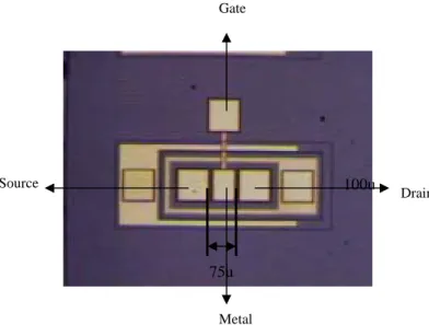
Figure 1. The two-emitter HBT device for measuring ledge thickness, emitter doping profile and collector doping profile. The two emitters are used as drain and source while the interconnect metal is used as the gate metal for the ledge between two emitters.
0.050 0.055 0.060 0.065 0.070 1E17
1E18 1E19
Emiiter doping profile Doping(cm-3)
Do ping d e ns it y (c m -3) Depth(um)
Figure 2. The emitter doping profile obtained through C-V measurement. 0.3 0.4 0.5 0.6 1E15 1E16 1E17 1E18
Collector Doping profile Doping(cm-3
) Doping dens it y (cm -3) Depth(um)
Figure 3. The collector doping profile obtained through C-V measurement. 0.035 0.040 0.045 0.050 0.055 0.060 1E17 1E18 1E19 1E20
Fat-FET doping profile doping(cm^-3)
D opi ng de ns it y( cm -3) Depth(um)
Figure 4. The ledge thickness measurement.
0 1 2 3 4 5 6 7 -0.002 0.000 0.002 0.004 0.006 0.008 0.010 0.012 0.014 0.016 0.018 123 4 5 6 7 8 9 10 1112 131415161718192021222324252627282930313233343536373839404142434445464748495051525354555657585960616263646566676869707172737475767778798081828384858687888990919293949596979899100101 ABC D E F G H I J
KLMNOPQRSTUVWXYZAAABACADAEAFAGAHAIAJAKALAMANAOAPAQARASATAUAVAWAXAYAZBABBBCBDBEBFBGBHBIBJBKBLBMBNBOBPBQBRBSBTBUBVBWBXBYBZCACBCCCDCECFCGCHCICJCKCLCMCNCOCPCQCRCSCTCUCVCW
abc d e f g h i j k
lmnopq r s t uvwxyzaaabacadaeafagahaiajakalam
anaoapaqarasatauavawaxayazbabbbcbdbebfbgbhbibjbkblbmbnbobpbqbrbsbtbubvbwbxbybzcacbcccdcecfcgchcicjckclcmcncocpcqcrcsctcucvcw
Ib=0uA Ib=10uA Ib=20uA Ib=30uA Ib=40uA Ib=50uA Ib=60uA Ib=70uA Ib=80uA Ib=90uA Ib=100uA Ib=110uA Ib=120uA Ib=130uA Ib=140uA Ib=150uA 1 Ib=160uA A Ib=170uA a Ib=180uA Ib=190uA Ib=200uA Ic( A ) Vce(volt)
Figure 5. I-V curve of 2.4X3X2 HBT device.
0.0 0.2 0.4 0.6 0.8 1.0 1.2 1.4 1.6 1E-12 1E-11 1E-10 1E-9 1E-8 1E-7 1E-6 1E-5 1E-4 1E-3 0.01 0.1 1 ForwardIB ForwardIC ReverseIB ReverseIC Cu rr e n t Vbe(volt)
Figure 6. GUmmel plot of 2.4X3X2 HBT device.
Gate Metal Source Drain 75u 100u
0.000 0.002 0.004 0.006 0.008 0.010 0.012 0.014 0.016 0.018 5 10 15 20 25 30 35 40 Vc=0.5V Vc=1.0V Vc=1.5V Vc=2.0V Vc=2.5V Vc=3.0V F t(G H z ) Ic(A) Figure 7. Cutoff frequency as a funvtion of collector current with collector-emitter voltage as a parameter
0 200 400 600 800 1000 1200 1400 2 3 4 5 6 7 8 9 10 11 12 Vc=0.5V Vc=1.0V Vc=1.5V Vc=2.0V Vc=2.5V Vc=3.0V tec (psec) 1/Ic(1/Amp)
Figure 8. A plot of emitter-collector charging time as a function of the reciprocal of collector current. The plot can be used to extrapolate the sum of base-transit time and base-collector transit time.
0.0 0.1 0.2 0.3 0.4 0.5 0.6 0.7 2.0 2.5 3.0 3.5 4.0 4.5 5.0 tB +X dep /2 Vs (p s e c) Xdep(um)
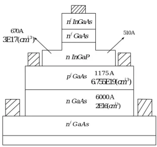
Figure 9. A plot of the sum of base-transit time and base-collector transit time as a function of the depeltion width. The plot can be used to extrapolate the base transit time. GaAs n+ n G aA s+ n GaAs p GaAs+ n InGaAs+ n InGaP 1 1 7 5 A D 3 6.755E19(cm−) 6000 A D 510A D 670A D 3 2E16(cm−) 3 3E17(cm−)
Figure 10. The HBT layer structure including ledge determined by the DC and RF measurements.