!"#"$"%"&"'"
()*+',"()-./012"
0
"
1
"
3
"
4
"
" " "56789:8;<=>"
"
Placement for Nanometer Low Dropout Regulators
"
"-.?@ABC"
""DEFG@HIJ""K1"
"
"
"
" " "L"M"N"!"O"P"Q"R"S"T"
56789:8;<=>"
Placement for Nanometer Low Dropout Regulators
- . ?@ABC Student@Jui-Pin Zheng
DEFG@HIJ Advisor@Hung-Ming Chen
! # $ % & '
( ) * + ' , ( ) - . / 0 1 2
0 1 3 4
A Thesis
Submitted to Department of Electronics Engineering and Institute of Electronics
College of Electrical Engineering and Computer Science
National Chiao Tung University
in partial Fulfillment of the Requirements
for the Degree of
Master of Science
in
Electronics Engineering
July 2009
Hsinchu, Taiwan, Republic of China
!"#$%&$'()*+
,-./01+
+
2345.678+9:+
+
+
;<=>?,@ABC,D+@AEFGH:I+
J
K
+ + + + + + +
+
LMNOP(QRST@U(VWXLYZ[\]^2_`(abc
_d@U(efgh^ijklRm(Bno^pq`(abTrstT
uv@UwK?x(yz{|}b(ef~C{•g€•C‚Rcƒ„&
O(uv@UwKk…(yz†C‡Dˆ‰Š‹Œgh•C•Ž•@${
|•‘’Xo“”r•?(–—c˜™•Cš›!"œ•T@U•žŸ
“”¡>¢£€o¤a¥¦#§c
hi‡uv@U¦¨_d@Uƒ©^‚ª (ef†CT«¬-®i
ƒ„lRm(ef{|¯°†C±²{#$%&$'h³Ac«¬(´µ
¶·¸¹º»¼`T½¾¿ÀmT{|ÁÂÃÄ`T±²{BÅef•‘
ÆÇÈ›TÇÉ«¬()*'Ã{€ÊLÆËBÅÊÌc
Placement for Nanometer Low Dropout Regulators
Student!Jui-Pin Zheng
Advisors!Dr. Hung-Ming Chen
Department of Electronics Engineering
Institute of Electronics
National Chiao Tung University
ABSTRACT
As are motivated by Moore’s law, the circuit complexities for VLSI
system are growing exponentially in the past decades. Digital designs are
benefited from many powerful automatic design tools. However, the analog
counterpart still demands huge engineering efforts and lengthy design period for
technology migration. For a robust analog design may require several iterations
to fulfill all the system specifications under process, voltage, and temperature
variations, this scenario may become worse since many short channel effects are
more pronounced as the devices step into the nanometer arena.
In order to bridge the gap between analog and digital VLSI design
capability, this work presents a framework for analog IP automatic design and
layout synthesis. Employing low drop out regulator as a vehicle, the placer can
generate a compact and regular layout a given circuit topology. In contrast to
solving many overlooked circuit equations, the proposed complier is based on
analog expert system concept and combines with simulated annealing. It can
achieve the target goals for the first time right without time-consuming iterations.
The layout synthesis part also automatically takes many design constraints for
device matching and area optimization into considerations. To verify the
performance of the placer, industrial cases are used to verify the correctness and
quality of the resulting layout. The experimental results showed that our
methodology can successfully apply to practical cases with rather compact and
regular placement.
!
"
# # # # # # ###
# # # #$%&'()*+,-'./012345678,9:0;<=6>?
@()ABCD,E@FGH0CIJKLMNNOO
XD
PQ9:R,STUPV
IC WX,YZ[\]^_`abcd0efKg
heijkZ[\]lm,nopqrstu@vfwexy0
EDA z
{,|}0~•€_•~f‚xƒ,STz„…xƒ„†‡ˆ‰Š‹0g
Œ•Ž|•,•+‘’“b”•m–—
VDA lab˜9:™,~•šE.›,
œ•‚ž0Ÿ ,¡
VDA ¢£¤¥,¦_§¨KLM©ª«™,¬FG
H-®˜
¯°±20²):,³´µ¶0·‚¸¹ºf0
IC WX»¼ˆiX½,¡
¾Y%U¿À0ÁÂÃÄWX•Ž.ÅÆ·_u*0+ǘ@ÈÉX½0
…ÊË,¾_µ·Ì'§¨ÍÎ0RÏNÐ,¾ÑÒ6Ó"ÔÕÖ×ØÙ
Ú×ÛÜÝ9ÞKß•Žàáâ~•0„Ð,¡¾@ãäåæç_èß,
éê¦6Ó"¾0ëìíîï•Žðñò,@X½Ë¾óôõö÷,øù
¦ôõèߘºú¦ºÓ"0toeàûƒ~•,@9:üJý¾þ¨ÿ
!•ŽÕæ˜
Ó"FGH0"#•ŽKLMó,JF GHþ¤¥0$%,•Žõô&!
èß0'(˜
Ó"¾0)*ó,J¾+,-þf0ö÷,•Ž.¾/0012
XD
Ó"¾03•,@¾T+KŒ4567‹,¡¾_É89E;0:;<˜
Love you all!
!"#$%#$&'
!()#%&%'*+&$,-.$ //////////////////////////////////////////////////////////////////////////////////////////////////////)' 0#12)&('*+&$,-.$ //////////////////////////////////////////////////////////////////////////////////////////////////////))' *.3#"42%516%#$&/ //////////////////////////////////////////////////////////////////////////////////////////////////)))' !"#$%#$& /////////////////////////////////////////////////////////////////////////////////////////////////////////////////)7' 8)&$'"9':-+2%&//////////////////////////////////////////////////////////////////////////////////////////////////////////7)' 8)&$'"9';)1<,%&////////////////////////////////////////////////////////////////////////////////////////////////////////7))' !(-=$%,'>' ' ?#$,"5<.$)"# /////////////////////////////////////////////////////////////////////////////////////// >' >/>' ' @%7)%4'"9'A,%7)"<&'B",3///////////////////////////////////////////////////////////////////////C' >/C' ' D<,'!"#$,)+<$)"#&//////////////////////////////////////////////////////////////////////////////////E' >/E' ' D,1-#)F-$)"#'"9':()&':(%&)& ///////////////////////////////////////////////////////////////////G' !(-=$%,'C' ' A,%2)6)#-,)%&/////////////////////////////////////////////////////////////////////////////////////// H' C/>' ' !"#$%6=",-,I'*#-2"1'A2-.%6%#$'@%=,%&%#$-$)"#&////////////////////////////////H' C/>/>' ' J%K<%#.%LA-),///////////////////////////////////////////////////////////////////////////////H' C/>/C' ' MNL:,%% ////////////////////////////////////////////////////////////////////////////////////////O' C/C' ' B),%2%#1$('P"5%2///////////////////////////////////////////////////////////////////////////////////O' C/E' ' Q)%,-,.().-2'J$,<.$<,% ////////////////////////////////////////////////////////////////////////////R' C/G' ' ;2"",=2-#'-#5'@"4LM-&%5'J$,<.$<,%//////////////////////////////////////////////////////S' C/H' ' A-.3)#1'"9'T"5%&////////////////////////////////////////////////////////////////////////////////// >>' C/O' ' ?5%#$)9I)#1'A,"U)6)$I/////////////////////////////////////////////////////////////////////////// >C' !(-=$%,'E' ' 0&&%#$)-2'A2-.%6%#$':%.(#)K<%&/////////////////////////////////////////////////////// >G' E/>' ' V%7).%'P%,1)#1 //////////////////////////////////////////////////////////////////////////////////// >G' E/C' ' 099",$'9",'@"<$)#1 //////////////////////////////////////////////////////////////////////////////// >W' E/E' ' B%22'0U$%#&)"# ///////////////////////////////////////////////////////////////////////////////////// >R'!"#$ $ %&'(')*+$,&-&+.)(*-"""""""""""""""""""""""""""""""""""""""""""""""""""""""""""""""""""""""""""""" /0$ !"1$ $ 2*')$34)(5(6.)(*- """""""""""""""""""""""""""""""""""""""""""""""""""""""""""""""""""""""""""""""" 78$ 9:.4)&+$#$ $ ;<4&+(5&-).=$%&'>=)' """"""""""""""""""""""""""""""""""""""""""""""""""""""""""""""""""""""" 7!$ 9:.4)&+$1$ $ 9*-?=>'(*-'$.-@$A>)>+&$B*+C' """""""""""""""""""""""""""""""""""""""""""""""""""""""" 7D$ E(F=(*G+.4:H """""""""""""""""""""""""""""""""""""""""""""""""""""""""""""""""""""""""""""""""""""""""""""""""""""""" 7I$ $ $
!"#$%&'%()*+,#%
!"#$%&'%(")*+,#%
-.-% % /01%2,#3+"0,#%4%#$+*3$*+,2%5643,7,8$.%9&754+,2%:"$;%/41<%:,%348%#,,% $;4$%$;,%#$+*3$*+,2%5643,7,8$%)+&*5#%3,66#%:"$;%,=*46%;,");$%482%:"2$;% $&),$;,+%$&%74>,%,43;%36*#$,+%7&+,%+,3$48)*64+ ...?% -.?% % @A,+A",:%&'%&*+%7,$;&2&6&)B ...C% ?.-% % D;,%&06"=*,%)+"2%482%'6&&+5648%&'%$;,%#,=*,83,E54"+%/!<%"1%F%/G%C%-%H% ?%I<%H%C%I%G%-%?1 ...H% ?.?% % J43>"8)%482%$+,,%0"84+B%$+,,%+,5+,#,8$4$"&8%&'%4%KLED+,,...M% ?.C% % D;"#%5"3$*+,%2,5"3$#%$;,%5"8E#,6,3$"&8%#3;,7,.%N43;%,82%&'%4%)4$,%348% 0,%$;,%5"8O%$;,+,'&+,<%:,%;4A,%$&%2,3"2,%:;"3;%,82%:"66%+,#*6$%"8%6,##% :"+,6,8)$;.%P,%:"66%3463*64$,%$;,%3,8$,+%&'%74##%:"$;%+,)4+2#%$&%466%$;,% ,82#%&'%)4$,#%"8%4%3,+$4"8%8,$%482%#,6,3$%'&+%$;,%,82#%:;"3;%348%6,42%$&% #7466,+%2"#$483,%/$&%3,8$,+%&'%74##1 ...M% ?.G% % @8,%;",+4+3;"346%36*#$,+"8)%,Q4756,.%N43;%2,A"3,%:"66%0,%36*#$,+,2%"8% &8,%&+%7&+,%)+&*5#<%482%,43;%36*#$,+%;4#%"$#%)+&*5"8)%5*+5&#,...R% ?.I% % S",+4+3;"346%6"#$%,Q4756,.%T,A"3,#%+,5+,#,8$,2%4#%8&2,#%4+,%6"8>,2%"8%4% 6"#$.%U*5,+8&2,%"#%4%8&2,%3&8$4"8"8)%7&+,%$;48%&8,%/#*5,+18&2,# ... --%?.H% % V8% "2,46% 34#,% &'% &*+% '6&&+5648.% N43;% :,66% +,)"&8% ;4#% +&*);6B% ,=*46%
:"2$;.%/01V%+,46"#$"3%34#,.%P"2$;%&'%,43;%:,66%+,)"&8%2"'',+#%"8%)+,4$%
+48),.%W&$,%$;4$%$;,%8*70,+%+,5+,#,8$#%'&+%$;,%#$4),%8*70,+%482%,43;%
+,3$48)*64+% &+% 5&6B)&8% 4+,4% &*$6"8,2% 0B% $;"3>% 0643>% 6"8,#% "#% 4% :,66%
!"#$ $ %&'$()*+,)-$&+./$(+00)1)2.$-'31,)-$4)15)($+2.'$'2)$(+-,3--+'2"$62$./+-$
,7-)8$ 7$ (3449$ 57.)$ &+./$ 4+2+434$ 0)7.31)$ -+:)$ &+;;$ <)$ +2-)1.)($
<).&))2$./)$.&'$()*+,)-$.'$<)$./)$,'22),.+25$<1+(5) """""""""""""""""""""""""" #=$
!">$ $ %/+-$ 0+531)$ ()?+,.-$ /'&$ &)$ ,'22),.$ 0+25)1-$ +2$ '2)$ 1)-+-.'1"$ %&'$
2)+5/<'1+25$,';342-$&+;;$2'.$<)$,'22),.)(@$+2-.)7(8$&)$A34?$'*)1$'2)$ $ 1'&$.'$47B)$7$1)-+-.'1$;''B$‘0';()("’$C'.)$./7.$./)$-.71.+25$72($)2($ ?'+2.$&+;;$<)$7.$2)+5/<'1+25$,';342-$70.)1$0+25)1$,'22),.+'2 """""""""""""" >#$ D"#$ $ E;7,)4)2.$1)-3;.$'0$,7-)$#"""""""""""""""""""""""""""""""""""""""""""""""""""""""""""""""""""" >D$ D">$ $ F'4?;).)($1'3.)($;79'3.$'0$,7-)$#""""""""""""""""""""""""""""""""""""""""""""""""""""""" >D$ D"!$ $ E;7,)4)2.$1)-3;.$'0$,7-)$>"""""""""""""""""""""""""""""""""""""""""""""""""""""""""""""""""""" >D$ D"D$ $ F'4?;).)($1'3.)($;79'3.$'0$,7-)$>""""""""""""""""""""""""""""""""""""""""""""""""""""""" >D$ D"=$ $ G$;79'3.$5)2)17.)($<9$HIJ%1))"""""""""""""""""""""""""""""""""""""""""""""""""""""""""""" >=$ $
Chapter 1
Introduction
Unlike the layout of digital circuits, analog layout is typically much more diffi-cult due to their sensitivities to circuit parasitic and physical implementation details. While coping with analog circuits, we have to consider circuit properties carefully; for example, we may try to put certain devices together to retain good matching between them, or we probably want to put couples of devices in symmetry to reduce the effect from process variation. In addition, different designers may have different views to the same circuits. The problems of analog layout automation have been studied for a long term, and the difficulty lies in topological constraints generation which could faithfully reflect what an analog designer wants. Cohn et al.[4] pointed out that the major topological constraints of analog placement are device symmetry, device matching, and device proximity. Symmetry constraints force devices to be symmetrical with respect to certain axis, and this helps reduce the effect of parasitic mismatches in differential circuits. Matching constraint usually exists within paired devices. When two devices need to be matched, they are usually designed to have equal width and equal length to assure equal nominal value. Proximity constraint clusters devices which need to locate in the same well or substrate together; more-over, devices which could be merged in the same diffusion will also be assigned to be placed near each other. This can effectively reduce design area and also help decrease the effect of substrate coupling.
Figure 1.1: (b) describes a structured placement. Compared with (a), we can see that the structured placement groups cells with equal height and width together to make each cluster more rectangular.
Analog placement usually does not follow the digital style. In fact, the perfor-mance of an analog circuit does rely on the design style and the design structure. As a result, regularity [9] of analog devices is also concerned during placement. For example, devices might be put in the same group if they could be extracted into a rectangular structure as shown in Figure 1.1 and sometimes the devices are required to be placed in the same orientation to achieve good matching.
1.1
Review of Previous Work
Automation of analog layout has been studied for many years. A conventional way to solve the problem is to use a constraint-driven approach. Charbon et al. [1] proposed a constraint-driven methodology which could automatically translate the electric performance specifications into constraints on layout parasitic for analog placement. Lampaert and Gielen proposed a performance-driven placement tool for analog integrated circuits [5]. In their approach, they first analyzed circuit proper-ties and then considered performance degradation within the placement methodol-ogy to avoid iterations between constraints extraction and layout generation. The performance-driven approaches can assure generated layout meet all high-level
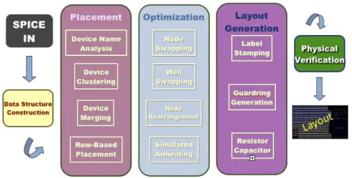
con-Figure 1.2: Overview of our methodology.
straints but the resulting cell layouts are not compact.
For topological constraints, Balasa and Lampaert [3] derived the symmetric-feasible constraints from the Sequence-Pair(SP) representation. Tam et al.[11] aug-mented the SP structure to consider symmetry constraints and other constraints simultaneously. Lin et al.[6] proposed the first amortized linear-time packing al-gorithm to tackle symmetry constraints based on B*-Tree. They later augmented their ideas to deal with matching, symmetry, and proximity constraints simultane-ously [7]. Nakatake [9] introduced a new concept of placement regularity to make the placement regularly arranged. Since placements with stronger regularity are much possible to be placed with few constraints, they thus proposed constraint-free analog placement [8]. Their methodology could formulate the topological complete symmetry structure without giving any symmetry constraints.
1.2
Our Contributions
In this work, we propose a complete methodology from analog device generation to placement. In order to attain better regularity, the devices are all with the same
unit width, and total width of a device will be adjusted by adding or removing gate fingers. Row-based structure is selected to be the basis placement structure. During the device generation stage, the transistors will be generated by the given attributes and technology information, such as additional dummy finger numbers or DRC information; as to the resistors, we assemble the resistors from arrayed fingers in order to obtain good matching.
The whole methodology flow is shown in Figure 1.2. A netlist file is first sized according to the required specification, and later fed to this procedure. After netlist analysis, we will identify device type, matching and proximity constraints, categorize stages, and cluster devices. A hierarchical row-based placement will be invoked as the next step with considering the constraints extracted in the previous step. Next, the optimization engine, which is a simulated annealing process, will try to minimize the placement area and reduce estimated routing wirelength. After the whole placement procedure, we will feed the information to our router and run physical verification to prove that our procedure can guarantee a LVS cleaned circuit with little DRC issues. The results can be shown on commercial layout editing tools.
1.3
Organization of This Thesis
The remainder of this thesis is organized as follows: Chapter 2 depicts prelim-inaries about analog placement constraints, wirelength model, and the row-based structure. Chapter 3 describes the essential placement techniques used in our al-gorithm and the complete alal-gorithm. Experimental results are shown in Chapter 4 and Chapter 5 concludes the contributions and future works.
Chapter 2
Preliminaries
We will introduce contemporary analog placement representations, our wire-length model, hierarchical structure used in analog placement, and the row-based structure used in our algorithm.
2.1
Contemperary Analog Placement
Represen-tations
Sequence-Pair and B*-Tree are introduced for being the representatives of con-temperary analog placement representations.
2.1.1
Sequence Pair
The sequence-pair representation of a floorplan is to encode a rectangle packing
as an ordered pair of module-name sequences (α, β). Suppose αi denotes the cell
occupying the ith position in sequence α, and α−1A states the position occupied by
αi. The topological relations between of two cells A and B are given as follows: if
α−1A < α−1B and βA−1 < βB−1, cell A is to the left of cell B; if α−1A < α−1B and βB−1 <
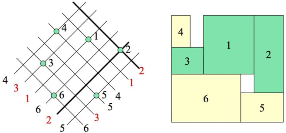
βA−1, cell A is above cell B. An example of 6 cells is show in Fig. 2.1. The sequence
is (α, β) = (4 3 1 6 2 5, 6 3 5 4 1 2) and we can observe that α3−1 < α−11 and β3−1
Figure 2.1: The oblique grid and floorplan of the sequence-pair (α, β) = (4 3 1 6 2 5, 6 3 5 4 1 2).
can be derived in O(n2), where n is the number of cells in the placement area. The
common way to explore the solution space is to use simulated annealing or genetic algorithm.
2.1.2
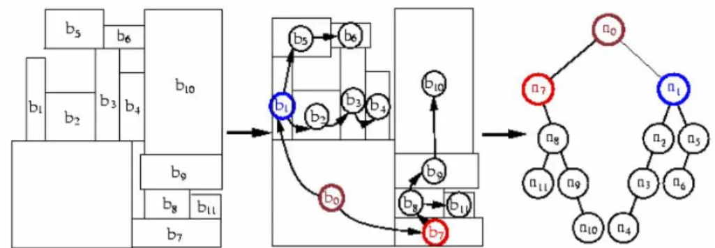
B*-Tree
A B*-Tree is an ordered binary tree representing a compact placement. Placing from the origin, the compact placement here states that if some force is given from top-right to bottom-left, each module will not move leftward and downward. The root of a B*-tree corresponds to the module residing at the bottom-left corner. For each node n corresponding to a module b, the left child of n represents the lowest, adjacent module on the right side of b, while the right child of n represents the first module above b with the same horizontal coordinate. A possible configuration is shown in Figure 2.2.
2.2
Wirelength Model
Our wire length estimation is based on HPWL approximation. Since polys (gates) can be connected by their two ends, we will decide which end will result in
Figure 2.2: Packing and tree binary tree representation of a B*-Tree.
Figure 2.3: This picture depicts the pin-selection scheme. Each end of a gate can be the pin; therefore, we have to decide which end will result in less wirelength. We will calculate the center of mass with regards to all the ends of gates in a certain net and select for the ends which can lead to smaller distance (to center of mass).
smaller wirelength by creating the center of mass of a net and choosing the ends closer to the center of mass. A possible configuration is shown in Figure 2.3. We have
4 gates with 4 pairs of pin candidates: (G1a, G1b), (G2a, G2b), (G3a, G3b), (G4a, G4b)
and G1b, G2a, G3b, G4a are selected because they are closer to the center of mass.
Note that fingers of gates are pre-connected in serpentine style during device gen-eration step, but the connection of sources and drains are solved in the routing stage.
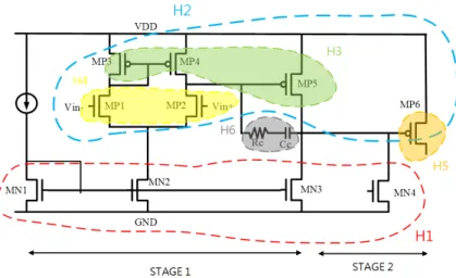
Figure 2.4: One hierarchical clustering example. Each device will be clustered in one or more groups, and each cluster has its grouping purpose.
2.3
Hierarchical Structure
While designing an analog circuit, it is not natural to view the whole circuit in a flatten aspect. Oftentimes, we group several devices together by certain purposes; for instance, devices may be grouped because they are in the same circuit block, or they might form a current mirror and need to be matched with each other. In many ways we might consider grouping devices together, but most of the time we do this for the following purposes:
1. To meet proximity constraint: When several devices belong to the same circuit division, or they are all of the same transistor type (PMOS or NMOS), they are better put together.
2. To meet matching constraint: Analog circuits typically rely on good compo-nent matching rather than accurate absolute values. For instance, designers may want to put equal-sized transistors that are used to generate a current mirror together.
3. To meet symmetry constraint: Devices may be set symmetric with respect to x-axis or y-axis, or both. Under this condition, moves of one block will result in corresponding moves to its paired block. One possible solution is to group them together and consider them as a bigger block.
Our hierarchical structure could be applied to deal with above constraints. The groups are pre-specified by designers. Within a general flow, PMOS and NMOS are generally in different potentials, so they form at least two groups. It is the very first and a very rough division. In Figure 2.4 , devices name which start with MP
will be in one group, and MN in another. We use H1={MP1, MP2, ..., MP6} and
H2={MN1, MN2, ..., MN4} to represent these devices. Also, capacitors and resistors
form another two groups, so we will have at least four groups in this hierarchy. For H1
and H2, we will collect devices which have the same well potential together because
the devices should not be taken apart. In our example, we have three well potentials
among the PMOS devices: H3={MP3, MP4, MP5}, H4={MP1, MP2}(differential
input), and H5={MP6}. Next, we will divide the devices into several subgroups
according to the pre-defined circuit sections. From this aspect, the first amplifier
stage H7 will contain {MP1, MP2, MP3, MP4, MN1, MN2}, second amplifier stage
H8 will contain {MP5, MN3, MN4}, and power mos H3={MP6}. Finally, we will
cluster passive devices such as resistors and capacitors in H6={Rc, Cc}.
2.4
Floorplan and Row-Based Structure
Floorplan of a circuit can be simply categorized into two classes; one is the slicing structure, and the other is the non-slicing structure. If we can repetitively divide the rectangles by horizontal or vertical cuts, the structure is called a slicing structure. Slicing floorplan is easy to maintain; in contrast, non-slicing floorplan is much more flexible while placing the devices but much difficult to maintain.
With corresponding to our equal-width design, we use a row-based floorplan to represent our placement. The representation is advantageous for the following reasons:
1. It is sliceable, so it is easy to maintain and implement.
2. It has strong regularity [Nakatake], so the resulting placement may be more acceptable by designers if they want to apply some changes to the layout manually.
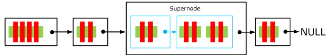
In the row-based structure, every row contains several devices which have the same width in sequence. The layout plane is made up with rows. In Figure 2.5, we can see that if several devices can be merged in the same diffusion, they are packed into a super device with the left-most device in this super device being the representative. Packing of a row can be processed by continuously inserting
MOS devices from left to right. During coordinate calculation, start by setting
the coordinate of the top-left device D0,0 to be the origin (0, 0), we can make its
immediate-right device D1,0 to be located at (0+width(D0,0), 0). Width of a super
device is determined as below:
Wsuperdevice= Σni=1Wi−dummy overhead + DRC overhead
where n is the total device number in the super device, dummy overhead is the total reduced dummy width during merging, and DRC overhead implies the minimum spacing between diffusions and other spacing.
The row-based structure is mainly applied to transistors; for the passive devices with greater widths and lengths (compared to the transistors), they are scattered at the sides of the control circuit (transistors), and this is what a designer often does. In order to improve routability and to prevent too congested layout, row utilization
Figure 2.5: Hierarchical list example. Devices represented as nodes are linked in a list. Supernode is a node containing more than one (super)nodes.
rate will be set to a value less than 1, usually between 0.7 and 0.9. The space in each row will be evenly distributed between devices.
2.5
Packing of Nodes
In order to implement the row structure mentioned above, we use a hierarchical linked-list to be our basic row. A simple representation is shown in Figure 2.5. Each node in the list can represent a MOS transistor, a capacitor, or a resistor; and each stores individual attributes, such as gate length, gate width, source/drain/bulk connections, nominal values, coordinates, and others. A node can also be cast as a hierarchical supernode, which is a packed node without containing any physical attributes. A supernode is used to pack several devices or other supernodes together to build up our hierarchy information. Packing of nodes is not difficult: we just have to assign the top-level nodes/supernodes into the list. During unpacking, we will scan the list from left to right and calculate for their coordinates. When we encounter a supernode, we need to traverse to its lower level to get end physical nodes. A multilevel traversal will be required because we have several hierarchies due to our circuit constraints and clustering principle. Origin of nodes in the top-level will be (0, 0); and if a node is packed by another supernode, its origin will be the bottom-left point its higher level parent. We do not keep the absolute coordinates of each node, and this will help us more easily update node positioning information
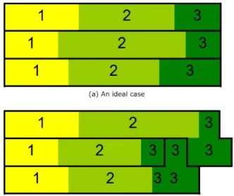
Figure 2.6: (a) An ideal case of our floorplan. Each well region has rouhgly equal width. (b)A realistic case. Width of each well region differs in great range. Note that the number represents for the stage number and each rectangular or polygon area outlined by thick black lines is a well region.
Merging mechanism. When we are dealing with the devices which are needed to be merged, what we do is to cluster the devices into a bigger block. The block itself still contains a smaller linked list, whose head is the left-most device of the merged devices. When we come to a merging block, we will know exactly what devices are contained, and they all can be processed at meanwhile. The processed merged devices will be set invisible to prevent device regeneration.
2.6
Identifying Proximity
Devices under several conditions will be required to abut with other devices, and the conditions may be as follows:
1. Devices which should locate in the same well must be clustered together to assure the continuity of well regions.
can help reducing wire length and also can boost the device-exchanging in one stage.
Since we are doing 2-D layouts, the solution to this problem can be viewed from two dimensions. Devices in the same well can be placed in x-direction sorted by their belonging stage number. This can preserve the continuity of the well. Similarly, wells are stacked in y-direction. The resulting floorplan will be as the one in Figure 2.6. Something needs to be mentioned that we give the placement a maximum width. In Figure 2.6(a), the ideal case, each of the wells has roughly the same width and total width in each stage of the well are roughly the same, so the resulting floorplan will have rectangular outline. But in Figure 2.6(b), a more realistic case, the difference of total widths of stages with each well ranges vastly, and some of the wells have exceed the total width limitation. In this case, wells exceed the width limitation will be folded directly down (or up) to its adjacent row, which means the exceeding devices will not be placed from the beginning of the adjacent row. Wells with the bigger value of total width will be placed in higher priority to make the placement process more regular. Note that the folding scheme is good for further optimization in exchanging devices because a well will not be broken into two or more discrete
segments. The resultant floorplan will have multiple hierarchies as shown in
the example and each hierarchy has its purpose. With the hierarchical clustering, we can easily generate a satisfiable floorplan that acts like going under a designers will.
Chapter 3
Essential Placement Techniques
We will describe our essential placement techniques in this section, including area minimization techniques, effort for routing difficulty relaxation, and device gen-eration.
3.1
Device Merging
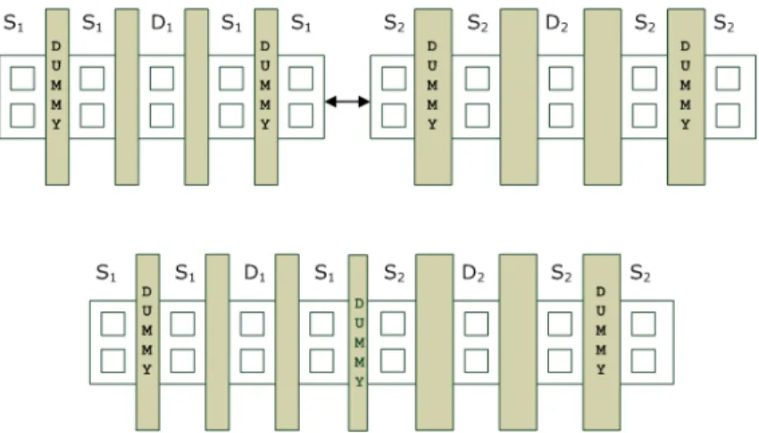
Devices form a current mirror usually can be merged in the same diffusion. During the placement procedure, we search in each stage for any mergeable devices. If any is found, we will try to bundle them as soon as possible. Device Merging is better done at the very beginning of the whole placement procedure; the reason is that merging will lead to total width reduction within a well region. If we execute this procedure later, well regions which exceed row limitation may have a chance to shrink and some space are squeezed out; in this case, we need to move devices to fill in the extra space, or we will waste them. The total width of one row is evaluated every time a device joins the row. To allow two devices merging without having the same source or drain, a dummy node is added to connect the two merging devices if they do not share same source or drain(Figure 3.1). Obviously, this approach can guarantee maximum use of row space and get rid of the possible space waste and
Figure 3.1: Two devices with different sources merged into one diffusion. In this case, a dummy gate with minimum feature size will be inserted between the two devices to be the connecting bridge.
redundant device moving.
The Device Merging Algorithm is shown below:
Procedure WidthAllocation
Input Device information and maximum width Output Width for all MOS devices and width
for all resistors, whose summation will not exceed the total width limitation
1. calculate total MOS area and resistor area 2. mos width := width limitation ;
3. res width := 0 ;
4. for mos width downto 0 step -10 do
5. res width := width limitation / mos width
6. mos height := mos area / mos width ;
7. res height := res area / res width ;
8. if ( mos height≈ res height ) break ;
9. end for
Algorithm Placement
Input Spice file with specified constraints Output Row-based placement
1. read in necessary files 2. build data structure 3. WidthAllocation() ; 4. GenInitSol() ; 5. for each row do
6. classify the devices into stages and sort them by stage numbers from
7. left to right ;
8. for each devices in row i do
9. put devices with the same merge group into the same diffusion
10. end for
11. calculate current row width ;
12. if ( current row width < max row limitation )
13. fetch devices located in next row to row i
14. if ( current row width > max row limitation )
15. push the rightmost devices directly down to next row until
16. row limitation is met
17. end for
The procedure WidthAllocation() aims at allocating equal height of MOS devices and resistors. Total MOS width is assigned to the value of maximum row width limitation. We use a loop to decrease the total MOS width value, and each time the value is decrease by a small number. Total MOS width and total resistor width are re-evaluated at each time of the loop, and the loop ends if the two width values are roughly the same. This guarantees the outline to be (or close to) rectangular.
3.2
Effort for Routing
In digital standard cell design, cell pins always locate on the upper and lower boundary (of a cell) and the pins are usually represented as a dot. In our methodol-ogy, gates within the same device are pre-routed (because the fingers always belong to the same net) during device generation stage, but sources and drains are extended and pins are labeled on each end for later routing. However, this will cause problems if we only report pins but ignore the leftover metal: other nets may go across the metal part and result in circuit short, or the other pin from the same net wants to connect to current pin but detours a lot because it does not know the metal it just crossed is within the same net. To make routing much simpler, we make several efforts as follows:
1. Pins are guaranteed to be on grid(track): the minimum unit of a layout cannot be infinitely small, hence, pins cannot be given in any coordinate and should be integer multiples of minimum unit specified in technology files; otherwise, we will get small shift from pin to interconnection when displaying on layout editing tools and will lead to design rule issues.
2. Leftover metals are set as pre-route: metals connected with the pins will be
set as pre-route. When we route net Ni, pre-routes belonged to net Ni will be
checked; if one pre-route has been crossed by any interconnect in the same net, the pin connected to this pre-route will not be forced routed. These pre-routes will be seen as blockage to other net.
3. Pin distribution: pin distribution such as polys, source/drain, and resistors are designed to make routing easier.
3.3
Well Extension
Wells in the same potential should be continuous on layout plane. Our placement algorithm would group devices within the same potential together, but space will appear after we add feedthroughs to a row. The Well Extension procedure will plant well regions between separated devices (but classified in same well). This operation is easy within a row: we just need to check if two neighboring devices are in the same well; if yes, we will plant a well region between them. Extension across two rows will be a little complex, but we can use the algorithm stated in below:
Algorithm Well Extension
Input Placement with segmented wells Output Placement with merged wells
1. foreach row ri
2. foreach device di,j in ri
3. if di,j and di,j+1 are in the same well
4. Calculate space (well region size)
5. Plant well
6. for each device di+1,k in ri+1
7. if overlap(di,j , di+1,k ) > 0
8. Plant well in the overlapped region
9. end for
10. end for
11. end for
3.4
Resistor Generation
Resistors are often built from a single finger and several fingers formed a resistor array. For a typical low dropout regulator, total value of resistors is usually ranging
from 500KΩ to 2000KΩ ; in this case, we select a 5KΩ-finger or a 10KΩ-finger to assemble the resistor array. In order to reduce wasted dummy resistors, we sort the resistor by numbers of fingers each resistor takes from large to small. Because the total width (of resistors) is limited to a number, which is derived from WidthAlloca-tion(), we will decide how many rows a resistor can occupy. The connection between each finger-column is designed to be the serpentine style. We do not directly connect two consecutive columns; instead, we jump over one column during connection to make a resistor folded. This scheme is explained in Figure 3.2
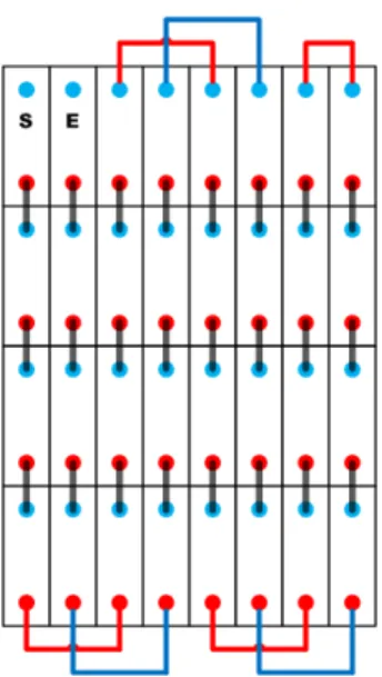
In Figure 3.2, S denotes the positive of the resistor and E denotes the negative.
After vertically connecting the fingers in any column Ci, we will skip Ci+1 and
connect Ci+2 with Ci. The arrows indicate the sequence we used to deal with this
resistor. Generally, we start from the positive and connect fingers which are in the
same column, say C0, with the positive. Next, we connect the bottom of C0 with
the bottom of C2 (skipping C1, because C1 will be processed later). Now is the
time to connect fingers in C2, so we go upward to connect them together. While
reaching the top of C2, we connect the top of C2 with the top of C4.When we reach
the right boundary of a resistor, we connect the columns backward so that the skipped columns will be processed later. Follow this scheme and we can guarantee the negative will always be in the direct neighboring column of positive and this will help to relieve the difficulty of routing since the resistor array is always located at the right side of controller circuit.
Procedure GenResistor
Input Resistor information and limited resistor width
Output Generated resistor array without exceeding the maximum resistor width 1. Sort resistors from large to small by their finger used
2. placed rows :=0
3. for i:=1 to num of res
4. if (Ri is placed) continue
5. for row:=2 to ∞
6. col := int( finger(Ri)/row )
7. curr width := col
8. if ( col*col width¡=res width )
9. Place Ri ;
10. placed rows := placed rows+Row(Ri)
11. break
12. for j:=i+1 to num of res
13. curr width := curr width + Col(Rj)
14. if ( col width*curr width<res width )
15. Place Rj
3.5
Post Optimization
Our optimization process is based on the simulated annealing algorithm and aims
at minimizing total wire length. The evaluation function is cost = α× W + Area,
where α is the experimental constant and W is the wirelength estimated under our model. Since we have a hierarchical structure, optimization can be done within a stage (in the same potential) and within a hierarchical merged module.
Figure 3.2: This figure depicts how we connect fingers in one resistor. Two neigh-boring columns will not be connected; instead, we jump over one row to make a resistor look ‘folded’. Note that the starting and end point will be at neighboring columns after finger connection.
be swapped with the others. The device can be the one that has not been clustered with others, or can be a hierarchical super node. The swapping must be executed in the same well to make sure we will not mess up the continuity of well potentials.
• Module Optimization Devices within a hierarchical module can also be swapped.
We apply the following set of moves to perturb the placement configuration:
1. Swapping two nodes : Nodes in the same well potential can be picked randomly and swapped. We assign different possibilities for nodes belonging two different stages. Nodes in the same stage are more possible to get swapped.
2. Swapping two wells : Before applying this huge operation, we will first detect if the swapping will result in well discontinuation. If not, the swapping can be applied directly; if yes, we will re-place the nodes. Re-placement will be more efficient than moving nodes (since it is just a process of putting nodes in
the list!). As a result, the operations result in segmented wells will have lower priority to be processed.
3. Rearranging Nodes : Nodes packed in supernodes can be swapped with each other. Since most of the time, the number of nodes in supernodes is not large; we generate all permutation and pick the best configuration (within the supernode).
Note that node rotation is not needed (some papers adopted this move) because devices with different directions will have bad effect on matching.
Chapter 4
Experimental Results
We applied our algorithm on realistic industrial designs. With different device size configurations, we will demonstrate how our methodology can generate regular layout planes and the efforts to ease routing. Things worth noting are that all our layouts (after our router) are guaranteed to be LVS cleaned. All the experiments are performed on a WinNT system under AMD AthlonX2 4800+ and 2048MB RAM. The whole procedure starts from automatic device sizing, placement, optimization, and routing. The results are shown on third-party commercial tools to help verify the correctness and quality of our layout.
Circuit with different sizing will result in different number of merge groups. In this case, we have about 70 transistors, 6 resistors(with variable values and fingers) and a big power mos. Total transistor width and resistor width are decided dynam-ically according to their values. Besides, all transistors are protected by guardrings to avoid noise coupling.
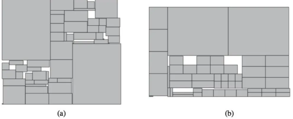
Figure 4.1 to Figure 4.4 show four layout snapshots of two configurations. We can see from the figures that our layout is very regular and different well regions do not break into segments. Figure 4.5 shows one layout generated under B*-Tree representation. It is difficult to compare our results with B*-Tree because of the following reasons:
Figure 4.1: Placement result of case 1. Figure 4.2: Completed routed layout of case 1.
Figure 4.3: Placement result of case 2. Figure 4.4: Completed routed layout of
case 2.
1. The B*-Tree layout is not regular. In order to make the layout regular, we have to manually slide the devices from their original locations. This manual operation will make wirelength estimation become worse and will also increase the difficulty of wirelength comparison.
2. Dead space produced and routability issue. B*-Tree squeezed the cells to min-imize area but resulted in poor routability in our case. However, we consider routability issue in our methodology and succesfully transform dead space into routing channels.
3. Device rotation is adopted in optimization process while analog devices usually are placed in one direction.
4. Device number is not equal because B*-Tree does not support device merging (OD Sharing).
Table 4.1: Experimental Results
Case Gate Width(µ) Device Groups Wirelength(µ) Area(µm2) Run Time(s)
1 0.9 34 12384.38 14038.2 9.26 2 0.8 33 68352.35 9337.8 5.28 3 2.8 36 9324.56 13521.1 8.07 4 0.8 35 10372.1 19263.8 14.3 5 1.2 35 8983.49 16783.6 12.8 6 0.9 40 9283.35 14134.4 10.91 7 2.4 43 14193.17 20131.2 13.35
Figure 4.5: A layout generated by B*-Tree.
Chapter 5
Conclusion and Future Work
We proposed a methodology to automatically generate a layout from netlist input file for low drop-out regulators. Device Merging and Well Sharing are used to compact layout area, Device Clustering is used to meet proximity constraints, and several additional techniques are proposed to relax the difficulties of routing. Our layout (after routing) can also be verified LVS cleaned on third-party commercial tools.
It is also possible to apply the algorithm to general purpose analog circuits if symmetry constraint is considered. A possible solution is to cluster devices needed to be paired in a supernode. Other device generation techniques such as gate folding scheme and gate arrangement can also be implemented to refine our placement results. Other future work such as transistor folding or support for constraint-less placement can also be considered to augment this work.
Bibliography
[1] E. Charbon, E. Malavasi, U. Choudhury, A. Casotto and A. Sangiovanni-Vincentelli , “A Constraint-Driven Placement Methodology for Analog In-tegrated Circuits,” IEEE Custom InIn-tegrated Circuits Conference, pp. 2821-2824, Boston, May 1992.
[2] F. Balasa , “Modeling non-slicing floorplans with binary trees,” Proc. IC-CAD, pp. 13–16, 2000.
[3] F. Balasa and K. Lampaert , “Module placement for analog layout using the sequence-pair representation,” Proc. DAC, pp. 274–279, 1999.
[4] J. M. Cohn, D. J. Garrod, R. A. Rutenbar, and L. R. Charley , “Analog device-level automation,” Kluwer Academic Publishers, 1994.
[5] K. Lampaert, G. Gielen, and W. M. Sansen , “A Performance-Driven Place-ment Tool for Analog Integrated Circuits,” IEEE J. Solid-State Circuits, vol. 30, no. 7, pp. 773-780, July 1995.
[6] P.-H. Lin and S.-C. Lin , “Analog placement based on novel symmetry-island formulation,” Proc. DAC, pp. 465–470, 2007.
[7] P.-H. Lin and S.-C. Lin , “Analog Placement Based on Hierarchical Module Clustering,” Proc. DAC, pp. 465–470, 2008.
[8] Qing Dong, S. Nakatake , “Constraint-free analog placement with topological symmetry structure,” Proc. ASP-DAC, pp. 186-191, 2008.
[9] S. Nakatake , “Structured Placement with Topological Regularity Evalua-tion,” Proc. ASP-DAC, pp. 215–220, 2007.
[10] Y.-C. Chang, Y.-W. Chang, G.-M. Wu, and S.-W. Wu , “B*-Trees: a new representation for non-slicing floorplans,” Proc. DAC, pp. 458–463, 2000.
[11] Y.-C Tam, Evangeline F. Y. Young, Chris C. N. Chu , “Analog placement with symmetry and other placement constraints,” Proc. ICCAD, pp. 349– 356, 2006.