IEEE ELECTRON DEVICE LETTERS, VOL. 29, NO. 8, AUGUST 2008 889
Novel Gate-All-Around Poly-Si TFTs With
Multiple Nanowire Channels
Ta-Chuan Liao, Student Member, IEEE, Shih-Wei Tu, Ming H. Yu, Wei-Kai Lin, Cheng-Chin Liu,
Kuo-Jui Chang, Ya-Hsiang Tai, and Huang-Chung Cheng, Member, IEEE
Abstract—The novel gate-all-around (GAA) poly-Si thin-film
transistors (TFTs) with multiple nanowire channels (MNCs) have been, for the first time, fabricated using a simple process to demonstrate high-performance electrical characteristics and high immunity to short-channel effects (SCEs). The nanowire channel with high body-thickness-to-width ratio (TFin/WFin), which is
approximately equal to one, was realized only with a sidewall-spacer formation. Moreover, the unique suspending MNCs were also achieved to build the GAA structure. The resultant GAA-MNC TFTs showed outstanding three-dimensional (3-D) gate con-trollability and excellent electrical characteristics, which revealed a high on/off current ratio (> 108), a low threshold voltage, a steep subthreshold swing, a near-free drain-induced barrier lowering, as well as an excellent SCE suppression. Therefore, such high-performance GAA-MNC TFTs are very suitable for applications in system-on-panel and 3-D circuits.
Index Terms—Gate-all-around (GAA), nanowire, poly-Si,
thin-film transistors (TFTs), three-dimensional (3-D) device.
I. INTRODUCTION
P
OLY-Si thin-film transistors (TFTs) have been widely used as switching elements in active matrix displays. For further system-on-panel (SOP) and 3-D circuit applications with high versatile circuit and system integration, there is a need to scale down poly-Si TFTs’ device geometries to achieve higher speeds and packing densities [1], [2]. Unfortunately, it has been shown that conventional planar (CP) short-channel poly-Si TFTs suffer from several undesirable short-channel effects (SCEs) in elec-trical characteristics, including threshold-voltage (Vth) roll-off, poor subthreshold swing (SS), and large drain-induced barrier lowering (DIBL), which greatly retard their applications [3], [4]. Recently, for single-crystalline-Si MOSFETs, lots of efforts on nonplanar device structures have been developed for better gate electrostatic control of the channel potential, such as double gated, triple gated, Π gated, Ω gated, nanowire channel,Manuscript received November 20, 2007. This work was supported by the National Science Council of Taiwan under Grant NSC 96-2218-E-009-010 and in part by the Chunghwa Picture Tubes. The review of this letter was arranged by Editor J. K. O. Sin.
T.-C. Liao, S.-W. Tu, M. H. Yu, W.-K. Lin, C.-C. Liu, K.-J. Chang, and H.-C. Cheng are with the Department of Electronics Engineering and the Institute of Electronics, National Chiao Tung University, Hsinchu 300, Taiwan, R.O.C. (e-mail: [email protected]; [email protected]; mhyuc@ tsmc.com; [email protected]; [email protected]; kuojuichang@ mail.nctu.edu.tw; [email protected]).
Y.-H. Tai is with the Display Institute, National Chiao Tung University, Hsinchu 300, Taiwan, R.O.C. (e-mail: [email protected]).
Color versions of one or more of the figures in this letter are available online at http://ieeexplore.ieee.org.
Digital Object Identifier 10.1109/LED.2008.2001176
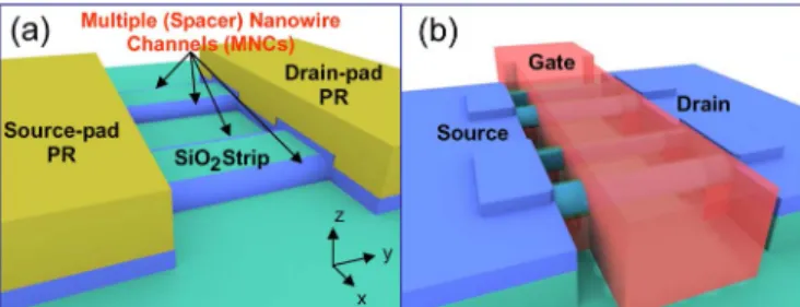
Fig. 1. Schematic diagrams of the key fabrication steps for GAA-MNC TFTs. (a) Formation of the MNCs and S/D pads. (b) Three-dimensional GAA formation.
and gate-all-around (GAA) [5]–[9]. Among those, GAA FETs, together with the nanowire channel, have been reported to be the best structure for extreme geometry scaling [7]–[9]. It is well known that poly-Si TFTs serve more pronounced SCEs than single-crystalline-Si MOSFETs due to the rich defects in poly-Si thin films [3], [4]. However, few works demonstrated such structures on poly-Si TFTs [10]–[12]. In this letter, we first apply a simple process to achieve the combined GAA and multiple-nanowire-channel (MNC) structures on poly-Si TFTs to improve the device performance and suppress the SCEs.
II. DEVICEFABRICATION
The key fabrication steps of the GAA-MNC poly-Si TFTs are schematically shown in Fig. 1. At first, a 50-nm-thick SiN and a 300-nm-thick tetraethyl orthosilicate (TEOS) SiO2were sequentially deposited by low-pressure chemical vapor deposi-tion (LPCVD) system at 780◦C and 700◦C on oxidized silicon wafer as a selectively etch-stop and a sacrificial layer, respec-tively. The sacrificial SiO2layer was then patterned with several dummy strips and anisotropically etched only at 100-nm depth to form the step profiles. After a 100-nm-thick a-Si conformal deposition by LPCVD at 550 ◦C, only the photoresists (PRs) for the source/drain (S/D) pads were patterned to overlap on the two edges of those dummy strips by standard g-line lithography. Subsequently, a reactive ion etch (RIE) (with a transformer-coupled RF power of 250 W and a standard capacitively cou-pled RF bias power of 150 W) was used to remove the a-Si; meanwhile, a couple of spacer nanowire channels were in situ resided in a self-aligned manner against the sidewall of each dummy strip and naturally connected to the S/D pads [Fig. 1(a)]. It should be noted that the nanoscale dimension of the nanowire channels can be defined only by controlling the RIE time without any advanced lithography [11]–[13], and the
890 IEEE ELECTRON DEVICE LETTERS, VOL. 29, NO. 8, AUGUST 2008
Fig. 2. (a) SEM image of the suspending spacer nanowire channel braced by S/D pads. (b) Cross-sectional TEM image of each channel of GAA-MNCs.
MNCs can be designed with patterning several dummy strips. After the release of S/D-pad PRs, a solid-phase crystallization at 600◦C in N2ambient for 24 h was performed to transform the a-Si into poly-Si. Then, the unique suspending MNCs were constructed after the dummy SiO2 strips were etched away (down to the SiN etch-stop layer) by an HF etchant. Then, the 25-nm-thick TEOS SiO2 and 200 nm of phosphorous in situ doped poly-Si (with a doping level of 5× l019cm−3) were con-formally deposited by the LPCVD system at 700◦C and 550◦C as gate insulator and gate electrode, respectively. After gate patterning, a self-aligned phosphorous S/D implantation was performed (at 30 keV to a dose of 5× 1015cm−2) [Fig. 1(b)], and a 300-nm-thick passivation oxide layer was deposited, followed by an S/D activation at 600◦C in N2ambient for 10 h. Contact opening formation, metallization, and 1-h NH3plasma passivation at 300◦C was carried out [14]. For the purpose of comparison, the CP poly-Si TFTs were also fabricated with the same process run.
III. RESULTS ANDDISCUSSION
Fig. 2(a) shows the scanning electron microscopy (SEM) image of the suspending spacer nanowire channel braced by S/D pads after the removal of dummy strips, and the empty space between the suspending nanowire channel and the etch-stop SiN layer is clearly observed. Fig. 2(b) shows the cross-sectional transmission electron microscopy (TEM) image of each GAA-MNC. The good step coverage is observed on the GAA structure both for the TEOS gate oxide and the phos-phorous in situ doped poly gate, and the vertical sidewall
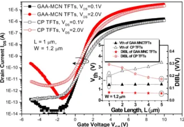
Fig. 3. Transfer characteristics of GAA-MNC and CP TFTs. The inset shows the comparisons of (left) Vthand (right) DIBL between GAA-MNC and CP
TFTs for different gate lengths.
thickness (TFin), the horizontal width (WFin), and the bevel length of each nanowire channel are about 85, 85, and 130 nm, respectively. Thus, the total surrounding width of each nano-wire channel is 300 nm. The aspect ratio TFin/WFin of each nanowire channel in the GAA-MNC TFT (approximately equal to one) is much larger than that in the CP TFT and thus features like a fin structure [6], [14].
Transfer characteristics of GAA-MNC and CP TFTs are compared in Fig. 3. Those devices have a gate length (L) of 1 µm and a channel width (W ) of 1.2 µm, where the W of GAA-MNC TFTs are defined by four nanowires with two-dummy-strip structure (2 strips× 2 wires/strip × 300 nm/wire = 1.2 µm). Vth was defined as the gate voltage that is required to obtain a normalized drain current of IDS= (W/L)× 10−8A at VDS= 0.1 V. SS was extracted at VDS= 0.1 V, and the maximum on current (Ion), the minimum off current (Ioff), and the maximum on/off current ratio (Ion/Ioff) were defined at VDS= 2.0 V. The field-effect mobility (µ) was extracted from the peak linear transconductance at VDS= 0.1 V. DIBL was defined as ∆VGS/∆VDS at IDS= 10−10A. Due to the inherently larger surface-to-volume ratio and the smaller volume of nanowire in the GAA-MNC TFT, fewer grain-boundary defects exist in the nanowire channels, leading to the lower minimum Ioff, higher maximum Ion, lower Vth, higher µ, and better SS [10]–[12], [16]. Moreover, the MNC scheme can also provide a more efficient NH3 plasma passi-vation to reduce the defects and further improve the minimum
Ioff, maximum Ion, Vth, µ, and SS characteristics [10], [14]. In addition, the 3-D fully surrounding gate (GAA) and the three sharp corners of the spacer profile in GAA-MNC TFTs effectively increase the gate controllability, resulting in higher performance on Ion, Vth, SS, µ, and DIBL as well [5], [17], [18]. Therefore, obvious improvement in device characteristics is achieved for the GAA-MNC TFT as compared with the CP TFT. Vth decreases from 2.23 to 1.41 V, SS decreases from 0.66 to 0.36 V/dec, minimum Ioffdecreases from 2.72× 10⁻¹² to 2.14× 10⁻¹³A, maximum Ionincreases from 2.21× 10⁻⁵ to 3.12× 10⁻⁵ A, Ion/Ioff increases from 8.12× 10⁶ to 1.46× 10⁸, µ increases from 18.8 to 25.5 cm2/V· s, and DIBL
LIAO et al.: NOVEL GATE-ALL-AROUND POLY-Si TFTs WITH MULTIPLE NANOWIRE CHANNELS 891
decreases from 0.3 to 0.06 V/V. In addition, the trap densities (Nt) were extracted from the slope of ln(IDS/VGS) versus
(1/VGS) according to the grain-boundary trap model [19]. It can be found that the GAA-MNC TFT exhibited a lower Nt
(1.1× 1012cm−2) than the CP TFT (1.5× 1012cm−2). This result further confirms the defect reduction in the GAA-MNC TFT. However, theOFF-state leakage current of the GAA-MNC TFT increases more rapidly than that of the CP TFT as the gate voltage decreases continuously, which is also explained by the higher electric field near the drain junction enhanced from these three sharp corners. It could be further improved by using the lightly doped drain or the T-shaped gate structures [20]–[22].
In addition, the inset of Fig. 3 shows the comparisons of Vth (left) and DIBL (right) between GAA-MNC and CP TFTs for different gate lengths. GAA-MNC TFTs exhibit negligible Vth and DIBL shifts as compared with those of CP TFTs, which is also attributed to the stronger gate controllability from both the 3-D GAA structure and the three sharp corners of the spacer nanowire that weakens the electric field penetration from the drain to the channel to efficiently suppress SCEs.
IV. CONCLUSION
The novel GAA-MNC TFTs have been demonstrated by using a simple process sequence. The MNCs were performed only with a sidewall-spacer formation. Furthermore, the unique suspending MNCs were also achieved to build the GAA struc-ture. Owing to the nanoscale dimension and the three sharp corners of the spacer nanowire, the 3-D GAA structure, to-gether with the more effective plasma passivation of such an MNC scheme, the GAA-MNC TFTs reveal high-performance characteristics and excellent SCE immunity. Therefore, such TFTs are highly promising for applications in SOP and 3-D circuits.
ACKNOWLEDGMENT
The authors would like to thank the National Nano Device Laboratories (NDL) for assistance in device fabrication and W.-L. Chen of Sino-American Silicon Products Inc. (SAS) for her technical assistance.
REFERENCES
[1] K. Banerjee, S. J. Souri, P. Kapur, and K. C. Saraswat, “3-D ICs: A novel chip design for improving deep sub-micrometer interconnect performance and system-on-chip integration,” Proc. IEEE, vol. 89, no. 5, pp. 602–633, May 2001.
[2] B.-Y. Tsui, C.-P. Lin, C.-F. Huang, and Y.-H. Xiao, “0.1 µm poly-Si thin film transistors for system-on-panel (SoP) applications,” in IEDM Tech.
Dig., 2005, pp. 911–914.
[3] M. Hack and A. G. Lewis, “Avalanche-induced effects in polysilicon thin-film transistors,” IEEE Electron Device Lett., vol. 12, no. 5, pp. 203–205, May 1991.
[4] B. Iñiguez, Z. Xu, T. A. Fjeldly, and M. S. Shur, “Unified model for short-channel poly-Si TFTs,” Solid State Electron., vol. 43, no. 10, pp. 1821–1831, Oct. 1999.
[5] B. Doyle, B. Boyanov, S. Datta, M. Doczy, S. Hareland, B. Jin, J. Kavalieros, T. Linton, R. Rios, and R. Chau, “Tri-gate fully-depleted CMOS transistors: Fabrication, design and layout,” in VLSI Symp. Tech.
Dig., 2003, pp. 133–134.
[6] F.-L. Yang, D. H. Lee, H. Y. Chen, C. Y. Chang, S. D. Liu, C. C. Huang, T. X. Chung, H. W. Chen, C. C. Huang, Y. H. Liu, C. C. Wu, C. C. Chen, S. C. Chen, Y. T. Chen, Y. H. Chen, C. J. Chen, B. W. Chan, P. F. Hsu, J. H. Shieh, H. J. Tao, Y. C. Yeo, Y. Li, J. W. Lee, P. Chne, M. S. Liang, and C. Hu, “5 nm-gate nanowire FinFET,” in VLSI Symp. Tech. Dig., 2004, pp. 196–197.
[7] J.-T. Park and J.-P. Colinge, “Multiple-gate SOI MOSFETs: Device design guidelines,” IEEE Trans. Electron Devices, vol. 49, no. 12, pp. 2222–2229, Dec. 2002.
[8] S. Monfray, T. Skotniki, Y. Morand, S. Descombes, P. Coronel, P. Mazoyer, S. Harrison, P. Ribot, A. Talbot, D. Dutartre, M. Haond, R. Palla, Y. Le Friec, F. Leverd, M. E. Nier, C. Vizioz, and D. Louis, “50 nm-gate all around (GAA)–silicon on nothing (SON)-devices: A simple way to co-integration of GAA transistors with bulk MOSFET process,” in VLSI Symp. Tech. Dig., 2002, pp. 108–109.
[9] H. Lee, L.-E. Yu, S.-W. Ryu, J.-W. Han, K. Jeon, D.-Y. Jang, K.-H. Kim, J. Lee, J.-H. Kim, S. C. Jeon, G. S. Lee, J. S. Oh, Y. C. Park, W. H. Bae, H. M. Lee, J. M. Yang, J. J. Yoo, and Y.-K. Choi, “Sub-5 nm all-around gate FinFET for ultimate scaling,” in VLSI Symp. Tech. Dig., 2006, pp. 58–59.
[10] Y.-C. Wu, T.-C. Chang, C.-W. Chou, Y.-C. Wu, P.-T. Liu, C.-H. Tu, J.-C. Lou, and C.-Y. Chang, “Effects of channel width and NH3
plasma passivation on electrical characteristics of polysilicon thin-film transistors by pattern-dependent metal-induced lateral crystallization,”
J. Electrochem. Soc., vol. 152, no. 7, pp. G545–G549, 2005.
[11] H.-H. Hsu, H.-C. Lin, J.-F. Huang, and C.-J. Su, “Poly-Si nanowire thin-film transistors with inverse-T gate,” in Proc. Ext. Abstract SSDM, 2007, pp. 818–819.
[12] C.-J. Su, H.-C. Lin, H.-H. Tsai, H.-H. Hsu, T.-M. Wang, T.-Y. Huang, and W.-X. Ni, “Operations of poly-Si nanowire thin-film transistors with a multiple-gated configuration,” Nanotechnology, vol. 18, no. 21, pp. 1–7, May 2007.
[13] Y.-K. Choi, T.-J. King, and C. Hu, “Nanoscale CMOS spacer FinFET for the terabit era,” IEEE Electron Device Lett., vol. 23, no. 1, pp. 25–27, Jan. 2002.
[14] H.-C. Cheng, F.-S. Wang, and C.-Y. Huang, “Effects of NH3 plasma
passivation on n-channel polycrystalline silicon thin-film transistors,”
IEEE Trans. Electron Devices, vol. 44, no. 1, pp. 64–68, Jan. 1997.
[15] H. Yin, W. Xianyu, H. Cho, X. Zhang, J. Jung, D. Kim, H. Lim, K. Park, J. Kim, J. Kwon, and T. Noguchi, “Advanced poly-Si TFT with fin-like channels by ELA,” IEEE Electron Device Lett., vol. 27, no. 5, pp. 357–359, May 2006.
[16] S. Zhang, C. Zhu, J. K. O. Sin, J. N. Li, and P. K. T. Mok, “Ultra-thin elevated channel poly-Si TFT technology for fully-integrated AMLCD system on glass,” IEEE Trans. Electron Devices, vol. 47, no. 3, pp. 569–575, Mar. 2000.
[17] P. Sallagoity, M. Ada-Hanifi, M. Paoli, and M. Haond, “Analysis of width edge effects in advanced isolation schemes for deep submicron CMOS technologies,” IEEE Trans. Electron Devices, vol. 43, no. 11, pp. 1900–1906, Nov. 1996.
[18] A. Burenkov and J. Lorenz, “Corner effect in double and triple gate Fin-FETs,” in Proc. 33rd ESSDERC, 2003, pp. 135–138.
[19] J. Levinson, F. R. Shepherd, P. J. Scanlon, W. D. Westwood, G. Este, and M. Rider, “Conductivity behavior in polycrystalline semiconductor thin film transistors,” J. Appl. Phys., vol. 53, no. 2, pp. 1193–1202, Feb. 1982. [20] J. G. Fossum, A. Ortiz-Conde, H. Shicjijo, and S. K. Banerjee, “Anomalous leakage current in LPCVD poly-silicon MOSFETs,” IEEE
Trans. Electron Devices, vol. 32, no. ED-9, pp. 1878–1884, Sep. 1985.
[21] W. Y. So, K. J. Yoo, S. I. Park, H. D. Kim, B. H. Kim, and H. K. Chung, “Novel self-aligned LDD/offset structure for poly-Si thin film transistors,” in Proc. SID, 2001, pp. 1250–1253.
[22] T.-C. Liao, C.-Y. Wu, F.-T. Chien, C.-C. Tsai, H.-H. Chen, C.-Y. Kung, and H.-C. Cheng, “A novel poly-Si thin film transistor with the in-situ vacuum gaps under the T-shaped-gated electrode,” Electrochem.