IEEE ELECTRON DEVICE LETTERS, VOL. 31, NO. 11, NOVEMBER 2010 1239
A Novel p-n-Diode Structure of SONOS-Type TFT
NVM With Embedded Silicon Nanocrystals
Tsung-Yu Chiang, William Cheng-Yu Ma, Yi-Hong Wu, Kuan-Ti Wang, and Tien-Sheng Chao
Abstract—In this letter, for the first time, a novel p-n-diode (PND) structure of SONOS-type thin-film transistor (TFT) non-volatile memory (NVM) with embedded silicon nanocrystals (Si-NCs) in the silicon nitride layer using an in situ method is successfully demonstrated. This novel structure has many ad-vantages, including high density and suitability for 3-D circuit integration. Hot-electron injection and hot-hole injection are used as the program and erase methods, respectively. The sensing current of the three-terminal PND-TFT NVM is 10−7 A by the band-to-band tunneling current. A much larger memory window (> 12 V) and good data retention time (> 108s for 12% charge loss) are exhibited. The device appears to have great potential for system-on-panel applications.
Index Terms—Band-to-band tunneling (BTBT), nonvolatile memory (NVM), p-n diode (PND), silicon nanocrystal (Si-NC), thin-film transistor (TFT).
I. INTRODUCTION
N
ONVOLATILE memories (NVMs) have attracted much attention in electronic products. The demands of NVMs include ultrahigh density, large memory window, and good data retention. The tunneling oxide of floating-gate (FG) memory is difficult to scale below 7 nm, and FG memory experiences serious FG interference as the device is scaled down [1], [2]. Thus, conventional FG memories face the scaling-down issue and need to be improved.Recently, much effort has been devoted to exploring SONOS memories as an alternative to FG memories [3]–[7]. SONOS memories provide many advantages over conventional FG memories, including no FG coupling effect, better immu-nity to drain-induced turn-on effect, higher density, elimination of SILC, and ease of vertical scale-down [3]–[7]. However, a traditional MOSFET encounters problems as it is scaled down, including serious short-channel effect, larger DIBL, and acute punchthrough effect [8]–[10]. For these reasons, it is difficult to scale down and achieve high density with single-crystal MOSFET SONOS memory devices. Accordingly, in order to
Manuscript received April 6, 2010; revised July 8, 2010; accepted July 21, 2010. Date of publication September 7, 2010; date of current version October 22, 2010. This work was supported by the National Science Council, Taiwan, under Contract NSC 97-2221-E-009-152-MY3. The review of this letter was arranged by Editor W. T. Ng.
T.-Y. Chiang, Y.-H. Wu, K.-T. Wang, and T.-S. Chao are with the Department of Electrophysics, National Chiao Tung University, Hsinchu 30010, Taiwan (e-mail: [email protected]).
W. C.-Y. Ma is with the Institute of Electronics, National Chiao Tung University, Hsinchu 300, Taiwan.
Color versions of one or more of the figures in this letter are available online at http://ieeexplore.ieee.org.
Digital Object Identifier 10.1109/LED.2010.2064153
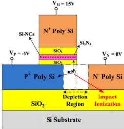
Fig. 1. Cross-sectional scheme of the PND-TFT memory structure with embedded Si-NCs using an in situ method.
achieve high density, thin-film transistors (TFTs) and special structures have been proposed and reported [11]–[13].
In this letter, for the first time, a p-n-diode (PND) structure of SONOS-type TFT memory with embedded silicon nanocrystals (Si-NCs) with good data retention using an in situ method has been successfully fabricated and proposed. The novel structure avoids the disadvantages of traditional single-crystal MOSFET SONOS-type memory devices, including serious SCE, larger DIBL, and acute punchthrough effect. Furthermore, with em-bedded Si-NCs in the nitride layer using the in situ method, the deep-trapped level can be created in the Si-NCs and the interface between the Si-NCs and silicon nitride [14]. Con-sequently, the data retention is improved, and the memory window is enhanced. For the aforementioned reasons, the PND-TFT memory with embedded Si-NCs in the nitride layer shows promise for future applications in multilevel operation, high-density, system-on-panel (SOP), and system-on-chip (SOC) technologies.
II. EXPERIMENTALPROCEDURE
A cross section of the PND-TFT memory device with em-bedded Si-NCs in the nitride layer is shown in Fig. 1. First, a 500-nm thermal oxide was grown on a 6-in silicon wafer using a furnace system. An undoped polysilicon layer with a thickness of 100 nm was deposited by low-pressure chemical vapor deposition (LPCVD). After patterning and defining the active regions, the active regions were implanted with boron (10 keV at 5× 1015 cm−2). Then, to form the ONO trilayer, an 8.5-nm tetraethyloxysilane (TEOS) tunneling oxide was
1240 IEEE ELECTRON DEVICE LETTERS, VOL. 31, NO. 11, NOVEMBER 2010
Fig. 2. Program speed characteristics of the PND-TFT memory at different operating voltage biases.
deposited by LPCVD. To sandwich Si-NCs in the silicon nitride layer, a Si3N4 (4-nm)/Si-NCs (by using SiH2Cl2, 10 sccm,
at 780 ◦C for 30 s)/Si3N4 (4-nm) multilayer of the trapping
layer was deposited using an in situ method by LPCVD [14]. A TEOS blocking oxide of about 15 nm was deposited by LPCVD. Next, a 200-nm n+ polysilicon as the gate electrode
was deposited and implanted with phosphorous (35 keV at 5× 1015 cm−2). A 100-nm TEOS oxide was deposited as a hard-mask layer. Then, after gate electrode patterning and definition, the n+ active regions were implanted with arsenic
(50 keV at 1× 1016cm−2) after the photolithography process. Subsequently, the PND-TFT memory was annealed in N2gas
at 950◦C for 10 s. The 500-nm TEOS oxide of the passiva-tion layer was deposited, and the contact hole was patterned. Finally, a 500-nm Al pad was deposited and patterned to finish the fabrication of the PND-TFT memory. The device with a polygate length (L) and an active width (W ) of 10 and 10 μm, respectively, was measured.
III. RESULTS ANDDISCUSSION
The PND-TFT memory was programmed and erased by using hot-electron and hot-hole injection mechanisms, respec-tively. However, hot carriers were produced using the im-pact ionization method. In the depletion region, the electrons were accelerated and obtained energy owing to the horizontal electric field under junction bias. A lot of hot-electron–hole pairs can be generated in the depletion region due to impact ionization of the accelerated electrons, as shown in Fig. 1. Figs. 2 and 3 show the program and erase speed characteristics under different operating biases. The program conditions were set at VG= 11, 13, 15 V, VN = 0 V, and VP =−5 V, while
the erase conditions were set at VG=−11, −13, −15 V, VN =
5 V, and VP = 0 V. In read mode, the sweeping of VGgenerates
a band-to-band tunneling (BTBT) current under a reverse bias of the p-n junction (VN = 0.3 V). The BTBT current represents
the sensing current. Read voltage (Vr) is defined as the applied
gate voltage when the sensing current is 10−7A in read mode. Memory window is defined as the Vr shift (ΔVr) between
the programmed and erased states. The ratio of the current at program state and the current at erase state is about three orders of magnitude. Under programming conditions, the electrons can tunnel from the P+ valence band to the depletion region
Fig. 3. Erase speed characteristics of the PND-TFT memory at different operating voltage biases.
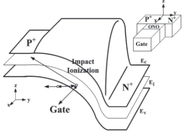
Fig. 4. Three-dimensional band diagram scheme of the PND-TFT memory structure with embedded Si-NCs at programming state.
along the y-axis by BTBT, as shown in Fig. 4. The tunneling electrons were accelerated by the horizontal electric field at reverse junction bias (at VP =−5 V). The hot electron can be
injected into the trapping layer and be trapped away from the depletion region along the x-axis by a positive gate voltage bias, as shown in Fig. 4. However, the hot hole can also inject into the trapping layer and be trapped by a negative gate voltage bias. The larger gate voltage bias tends to result in faster program and erase speeds owing to the increased vertical electric filed. After programming, the 12-V shift of Vrwas found. The lager
memory window (12 V) is sufficient for the application of multilevel operations. The programming speed and drain distur-bance should be traded off. So far, we are still trying to optimize the operation voltage. In this letter, the programming voltage (VG= 15 V, VN = 0 V, and VP =−5 V) can be shifted by
more than 3 V in 1 ms. According to the present literature, the programming speed of our PND is comparable [15].
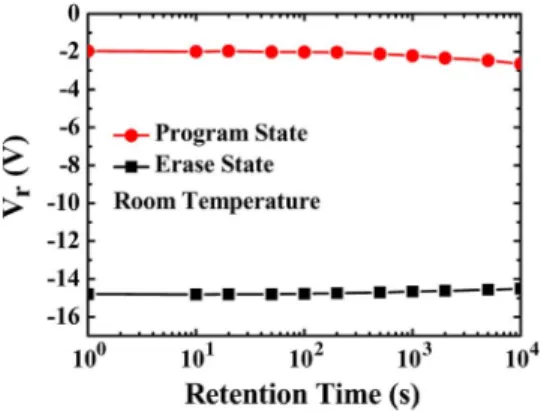
The data retention characteristics of the PND-TFT mem-ory device at room temperature are shown in Fig. 5. The program and erase states were set as the PND-TFT memory after programming at VG= 15 V, VN = 0 V, VP =−5 V,
1 s and erasing at VG=−15 V, VN = 5 V, VP = 0 V, 1 s,
respectively. The charge loss was below 5% for 104s, as shown in Fig. 5. Extrapolated to 108s, it exhibits only a 12% charge loss. The larger memory window and good data retention of the PND-TFT memory are very suitable for applications of high density, multilevel operation, and SOP, as well as 3-D circuit integration.
CHIANG et al.: NOVEL PND STRUCTURE OF SONOS-TYPE TFT NONVOLATILE MEMORY 1241
Fig. 5. Data retention characteristics of the PND-TFT memory when pro-gramming ΔVt= 12 V at room temperature.
IV. CONCLUSION
In this letter, a PND-TFT NVM with embedded Si-NCs in a novel structure, fabricated using an in situ method, has been reported and demonstrated for the first time. The PND-TFT memory may well represent a breakthrough in the problems involved in scaling down such devices. At the same time, the PND-TFT memory, which achieves 3-D multilayer stack memory, can carry out ultrahigh-density memory generation. The novel structure has excellent characteristics in terms of larger memory windows, good P/E efficiency, and longer data retention time. Therefore, the PND-TFT memory is an excellent candidate for SOP and SOC applications in the future.
ACKNOWLEDGMENT
The authors would like to thank the National Nano Device Laboratories and the Nano Facility Center of National Chiao Tung University for the process support.
REFERENCES
[1] E. K. Lai, H. T. Lue, Y. H. Hsiao, J. Y. Hsieh, C. P. Lu, S. Y. Wang, L. W. Yang, T. Yang, K. C. Chen, J. Gong, K. Y. Hsieh, R. Liu, and C. Y. Lu, “A multi-layer stackable thin-film transistor (TFT) NAND-type flash memory,” in IEDM Tech. Dig., 2006, pp. 1–4.
[2] C. Y. Lu, T. C. Lu, and R. Liu, “Non-volatile memory technology—Today and tomorrow,” in Proc. Symp. IPFA Circuits Dig., 2006, pp. 18–23.
[3] H. C. You, T. H. Hsu, F. H. Ko, J. W. Huang, W. L. Yang, and T. F. Lei, “SONOS-type Flash memory using an HfO2as a charge trapping layer
deposited by the sol-gel spin-coating method,” IEEE Electron Device
Lett., vol. 27, no. 8, pp. 653–655, Aug. 2006.
[4] K. H. Wu, H. C. Chien, C. C. Chan, T. S. Chen, and C. H. Kao, “SONOS device with tapered bandgap nitride layer,” IEEE Trans. Electron Devices, vol. 52, no. 5, pp. 987–992, May 2005.
[5] M. K. Cho and D. M. Kim, “High performance SONOS memory cells free of drain turn-on and over-erase: Compatibility issue with current flash technology,” IEEE Electron Device Lett., vol. 21, no. 8, pp. 399–401, Aug. 2000.
[6] P. Xuan, M. She, B. Harteneck, A. Liddle, J. Bokor, and T.-J. King, “FinFET SONOS flash memory for embedded applications,” in IEDM
Tech. Dig., 2003, pp. 609–613.
[7] T. Y. Chan, K. K. Young, and C. Hu, “A true single-transistor oxide-nitride-oxide EEPROM device,” IEEE Electron Device Lett., vol. EDL-8, no. 3, pp. 93–95, Mar. 1987.
[8] K. T. Toh, P. K. Ko, and R. G. Meyer, “A engineering model for short-channel MOS devices,” IEEE J. Solid-State Circuits, vol. 23, no. 4, pp. 950–958, Aug. 1988.
[9] R. R. Troutman, “VLSI limitations from drain-induced barrier lowering,”
IEEE Trans. Electron Devices, vol. ED-26, no. 4, pp. 461–469, Apr. 1979.
[10] S. G. Chamberlain and S. Ramanan, “Drain-induced barrier-lowering analysis in VLSI MOSFET devices using two-dimensional numerical sim-ulations,” IEEE Trans. Electron Devices, vol. ED-33, no. 11, pp. 1745– 1753, Nov. 1986.
[11] J. Sarkar, S. Dey, D. Shahrjerdi, and S. K. Banerjee, “Vertical flash memory cell with nanocrystal floating gate for ultradense integration and good retention,” IEEE Electron Device Lett., vol. 28, no. 5, pp. 449–451, May 2007.
[12] J. Sarkar, S. Tang, D. Shahrjerdi, and S. K. Banerjee, “Vertical flash memory with protein-mediated assembly of nanocrystal floating gate,”
Appl. Phys. Lett., vol. 90, no. 10, p. 103 512, Mar. 2007.
[13] T. Y. Chiang, M. W. Ma, Y. H. Wu, P. Y. Kuo, K. T. Wang, C. C. Liao, C. R. Yeh, and T. S. Chao, “A novel MILC-TFT with dual purpose of high performance device and one-time-programmable memory applications,”
IEEE Electron Device Lett., vol. 30, no. 9, pp. 954–956, Sep. 2009.
[14] T. Y. Chiang, T. S. Chao, Y. H. Wu, and W. L. Yang, “High program/erase speed SONOS NVM with in-situ silicon nanocrystal,” IEEE Electron
Device Lett., vol. 29, no. 10, pp. 1148–1151, Oct. 2008.
[15] Y. H. Lin, C. H. Chien, T. H. Chou, T. S. Chao, and T. F. Lei, “Low-temperature polycrystalline silicon thin-film flash memory with hafnium silicate,” IEEE Trans. Electron Devices, vol. 54, no. 3, pp. 531–536, Mar. 2007.