Long electron dephasing length and disorder-induced spin-orbit coupling
in indium tin oxide nanowires
Yao-Wen Hsu,1 Shao-Pin Chiu,1 An-Shao Lien,1and Juhn-Jong Lin1,2,
*
1Institute of Physics, National Chiao Tung University, Hsinchu 30010, Taiwan 2Department of Electrophysics, National Chiao Tung University, Hsinchu 30010, Taiwan 共Received 1 August 2010; revised manuscript received 27 September 2010; published 15 November 2010兲We have measured the quantum-interference magnetoresistances in two single indium tin oxide 共ITO兲 nanowires between 0.25 and 40 K, by using the four-probe configuration method. The magnetoresistances are compared with the one-dimensional weak-共anti兲localization theory to extract the electron dephasing length L. We found, in a 60-nm-diameter nanowire with a low resistivity of共10 K兲=185 ⍀ cm, that L is long, increasing from 150 nm at 40 K to 520 nm at 0.25 K. Therefore, the nanowire reveals strict one-dimensional weak-localization effect up to several tens of degrees of kelvin. In a second 72-nm-diameter nanowire with a high resistivity of共10 K兲=1030 ⍀ cm, the dephasing length is suppressed to L共0.26 K兲=200 nm, and thus a crossover of the effective device dimensionality from one to three occurs at about 12 K. In particular, disorder-induced spin-orbit coupling is evident in the latter sample, manifesting weak-antilocalization effect at temperatures below⬃4 K. These observations demonstrate that versatile quantum-interference effects can be realized in ITO nanowires by controlling differing levels of atomic defects and impurities.
DOI:10.1103/PhysRevB.82.195429 PACS number共s兲: 73.63.⫺b, 73.23.⫺b, 73.20.Fz, 73.20.Jc
I. INTRODUCTION
In weakly disordered metals and semiconductors共all real conductors are disordered兲, quantum-interference electron transport plays vital roles at liquid-helium temperatures.1
The quantum-interference phenomena, which originate from the inherent wave nature of the conduction electrons, become progressively pronounced as the temperature is lowered and the effective device dimensionality is reduced. In this regard, metal and doped semiconductor nanowires could provide a rich platform for probing novel, nonclassical properties and functionalities. In a random potential, the conduction elec-trons undergo Brownian-type diffusive motion, leading to various quantum-interference phenomena, including the weak-共anti兲localization effect, Aharonov-Bohm oscillations, universal conductance fluctuations, and persistent currents.2
Previously, such quantum-interference behaviors have mostly been investigated by utilizing submicron devices fab-ricated via the “top-down” electron-beam lithography technique.3
Compared with the temperature dependence of the resis-tance rise due to weak-localization and electron-electron in-teraction effects at low temperatures,4magnetoresistances
in-duced by small externally applied magnetic fields can provide very quantitative information about the inelastic electron 共electron-phonon and electron-electron兲 scattering and spin-flip 共spin-orbit and magnetic spin-spin兲 scattering mechanisms in a given nanowire device.5Therefore,
system-atic and careful measurements of magnetoresistances in the weak-共anti兲localization effect are indispensable and highly desirable for learning the responsible microscopic electron relaxation processes.6Reliable knowledge about the electron
relaxation processes can help in paving the way for the future realization of sensitive and versatile quantum-interference nanoelectronics and spintronics. Since as-grown metal and semiconductor nanowires often contain high levels of point defects,7,8 it is natural to expect that quantum-interference
effects should be pronounced in many “bottom-up” nano-structures.
Among the numerous metallic nanowires, Sn-doped In2O3 共indium tin oxide or ITO兲 nanowires have recently been studied.9–11The interest in these nanoscale structures arises
from the fact that the parent ITO material is a transparent conducting oxide. Moreover, the charge carriers in this ma-terial are established to be essentially free-electronlike.12
That is, the charge carriers behave like an ideal free-electron gas with an effective mass of mⴱ⬇0.4m and a small Fermi energy EFⱗ1 eV, where m is the free-electron mass. The thermoelectric power reveals a linear diffusive term from 300 K all the way down to liquid-helium temperatures while the temperature dependence of resistivity is well described by the Bloch-Grüneisen law at not too low temperatures.13 The carrier concentration in highly conductive ITO materials falls in the range 1020– 1021 cm−3,14 and the
room-temperature resistivity can be as low as
⬃100–200 ⍀ cm.9Therefore, ITO nanowires appear to be
attractive candidates for in-depth investigations of the quantum-interference electron transport. Surprisingly, to the best of the authors’ knowledge, the weak-localization mag-netoresistances in ITO nanowires has previously been re-ported only in one study in which the electrical measure-ments were performed on two-probe, rather than four-probe, individual nanowire devices.15 In that experiment, the
au-thors reported a very short electron dephasing 共phase-breaking兲 length, L, of 31共15兲 nm at 10 共100兲 K.
In this work, we have investigated low-temperature mag-netoresistances in the weak-共anti兲localization effect in one low-resistivity and one high-resistivity ITO nanowires, by employing the four-probe configuration method. The electron dephasing length Land the spin-orbit scattering length, Lso, are experimentally extracted. We found a very long
L共0.25 K兲⬇520 nm, which is considerably longer than
most electron dephasing lengths reported in previous studies of as-grown nanowires. Furthermore, we demonstrate that
the strength of spin-orbit coupling can be adjusted by modi-fying the level of disorder or electron mean-free path, l, in the nanowire. As a consequence, both the weak-localization effect 共which is characterized by negative magnetoresis-tances兲 and the weak-antilocalization effect 共which is char-acterized by positive magnetoresistances兲 can be “tuned” and visualized in ITO single nanowires in low magnetic fields.
II. EXPERIMENTAL METHOD
ITO 共In2−xSnxO3−y兲 nanowires were synthesized on Si substrates by the standard thermal evaporation method, as described previously.7 X-ray diffraction 共XRD, MAC
Sci-ence MXP-18兲 and high-resolution transmission electron mi-croscopy 共TEM, JEOL JEM-2010FX兲 studies indicated that the nanowires were single crystalline, possessing a cubic bix-byite structure, and grew along the 关100兴 direction. Energy-dispersive x-ray spectroscopy 共EDS, JOEL JEM-2010FX兲 and inductively coupled plasma atomic emission spectrom-etry共ICP-OES, Perkin Elmer Optima-3000DV兲 were utilized to determine the chemical compositions of the nanowires. We obtained an Sn/In weight ratio of⬃4.4%, confirming that Sn was effectively incorporated into the ITO nanowires.7
Both the electron-beam lithography and focused-ion beam 共FIB兲 techniques were employed to make four-probe indi-vidual nanowire devices for magnetoresistance measure-ments. We first made micron-sized Ti/Au 共10/60 nm兲 metal pads and coordinate marks by utilizing the standard photoli-thography and lift-off technique on a SiO2 layer 共400 nm thick兲 capped Si substrates. ITO nanowires were then dis-persed on the SiO2/Si substrates. Individual nanowires with diameters of ⬃60–70 nm were identified and electrically connected to the prepatterned micron-sized Ti/Au metal pads by using the standard electron-beam lithography and lift-off technique共for the ITO-r nanowire device兲. In order to make good ohmic contacts to the nanowire, O2 plasma was em-ployed to clean the substrate before the Cr/Au共10/100 nm兲 electrodes contacting the nanowire were deposited by the thermal evaporation method. A scanning electron microscope 共SEM兲 image of the ITO-r nanowire is shown in the inset of Fig.2.
To fabricate the four-probe ITO-f individual nanowire de-vice, we employed the FIB technique. In an FEI Dual-Beam
NOVA 200 FIB instrument, we applied the
Ga+-beam-induced deposition method with a methyl cyclo-pentadienyl trimethyl platinum 共CH3兲3Pt共CpCH3兲 injector to selectively deposit Pt metal for connecting the ITO nanowire with the Ti/Au pads. The Ga+ions were accelerated to 30 kV at 10 pA and injected into the nanowire during the Pt depo-sition. The dimensions of the Pt contacting electrodes were set 80 nm in width and 100 nm in thickness but the actual width was about 300 nm and the actual thickness was not determined. An SEM image of the four-probe ITO-f nano-wire device is shown in the inset of Fig.4.
The individual nanowire devices were placed on a sample holder which was situated inside a dark vacuum can. The vacuum can was mounted on an Oxford Heliox3He cryostat for magnetoresistance measurements from 40 K down to 0.25 K. The cryostat was equipped with a 4 T
superconduct-ing solenoid, and the temperature was monitored with cali-brated RuO2 and Cernox thermometers. An ac resistance bridge共Linear Research LR-700兲 was employed for the mea-surement of magnetic field dependent resistance, R共B兲, at various fixed temperatures. In all cases, the magnetic fields were applied perpendicular to the nanowire axis. A small measuring current 共ⱗ30 nA兲 was employed to avoid Joule heating. Linearity in the current-voltage curves was repeated checked and ensured.
III. RESULTS AND DISCUSSION
Figure 1 shows the normalized magnetoresistance, ⌬R共B兲/R共0兲=关R共B兲−R共0兲兴/R共0兲, as a function of magnetic field at several temperatures of the low-resistivity ITO-r nanowire. This figure reveals that the magnetoresistances are always negative, implying a very weak spin-orbit scattering rate relative to the inelastic electron-scattering rate even down to 0.25 K in this particular nanowire. Our measured low-field magnetoresistances were least-squares fitted to the one-dimensional weak-localization theoretical prediction4,16
⌬R共B兲 R共0兲 = e2 ប R L
再
3 2冋
冉
1 L2 + 4 3Lso 2 + W2 3LB 4冊
−1/2 −冉
1 L2 + 4 3Lso 2冊
−1/2册
−1 2冋
冉
1 L2 + W2 3LB 4冊
−1/2 − L册
冎
, 共1兲 where R is the resistance of a nanowire of width W and length L, LB=冑
ប/eB is the magnetic length 共ប is the Planck constant divided by 2, and e is the electronic charge兲,L=
冑
D is the electron dephasing length, Lso=冑
Dsois the spin-orbit scattering length, and D =vF2
e/3 is the electron diffusion constant17 共v
F being the Fermi velocity,18 and e being the electron mean-free time兲. Here and soare the electron dephasing time and the spin-orbit scattering time, respectively. The spin-orbit scattering length 共time兲 is a temperature-independent quantity whose size, relative to the
0.00 0.03 0.06 0.09 0.12 0.15 0.18 -0.009 -0.006 -0.003 0.000 ∆ R (B )/ R (0) B (T)
FIG. 1. 共Color online兲 Normalized magnetoresistance as a func-tion of perpendicular magnetic field of the ITO-r nanowire at共from bottom up兲: 0.25, 5.0, 12, 20, 30, and 40 K. The symbols are the experimental data and the solid curves are the theoretical predic-tions of Eq.共1兲.
inelastic scattering strength, determines the sign of the weak-共anti兲localization effects in the low-field magnetoresistance.4,19
In Fig.1, the symbols are the experimental data and the solid curves are the theoretical predictions of Eq. 共1兲. This figure clearly indicates that the measured magnetoresistances can be well described by the one-dimensional weak-localization theory in the wide temperature interval of 0.25–40 K. Therefore, the important characteristic electron-scattering lengths, Land Lso, can be accurately extracted. In this low-resistivity nanowire, we obtained an extraordinarily long Lso 共so兲. In other words, the spin-orbit interaction is negligibly weak 共absent兲, to within our experimental uncertainty, in this sample. 关We estimate the length
Lsoⲏ0.5 m, or the timesoⲏ1⫻10−10 s, in this nanowire 共see below兲. It is worth noting that this spin-orbit scattering length is comparable to or even longer than that in relatively clean Al films and wires.20兴
Figure2shows our extracted Las a function of tempera-ture for the low-resistivity ITO-r nanowire. The inset shows an SEM image of this individual nanowire device. This fig-ure indicates that L increases from 150 to 520 nm as the temperature decreases from 40 K down to 0.25 K.21 This
result bears significant implications. As a consequence of such a long L, the weak-localization behavior is purely one
dimensional in this particular nanowire device over our whole measurement temperature range. In fact, it is clear that the one-dimensional weak-localization behavior will persist up to much above 40 K. In contrast, in previous studies of individual nanowires made of ITO,15,22 and other materials
such as InAs 共Refs.23and24兲 and P-doped Si,25 the mag-netoresistance measurements were performed on two-probe configurations and the obtained L were often short 共ⱗ100 nm at 1 K兲. Thus, a crossover of the device dimen-sionality from one to three, in regard to the weak-localization effect, inevitably happens already at low temperatures of a few degrees of kelvin. Under such circumstances, the ex-tracted values of L 共兲 above a few degrees of kelvin are obviously questionable.
In a weakly disordered conductor, the electron dephasing time is given by5 1 共T兲= 1 0 + 1 ee共T兲 + 1 ep共T兲 , 共2兲
where0is a constant, whose origins共paramagnetic impurity scattering, dynamical structural defects, etc.兲 are a subject of elaborate theoretical and experimental investigations.16,26–29
The electron-electron relaxation rate,ee−1, in low-dimensional disordered conductors is known to dominate−1in an appre-ciably wide temperature interval.4,5 The electron-phonon
scattering rate,ep−1, will become important at high measure-ment temperatures. We use the standard expression:
ep−1= AepT2in the quasiballistic limit of qTl⬎1 共which is per-tinent to the present study兲,30,31where q
Tis the wave number of a thermal phonon and l is the electron mean-free path. The electron-electron relaxation rate was fitted in the form
ee−1= AeeTp. As it is shown in Fig. 2, the dependence L=
冑
D is well fitted by Eq. 共2兲 with four adjustable pa-rameters0, Aee, p, and Aep. Our fitted values of0 and Aep are listed in TableI. It should be stressed that we obtain an exponent of temperature p⬇0.68⫾0.10, which is very close to the theoretical value 共=2/3兲 of the Nyquist electron-electron scattering rate in one dimension. Moreover, our fit-ted value of Aee is in good agreement with the theoretical prediction of4,5,16 1 ee =冉
e 2冑
DRk BT 2冑
2ប2L冊
2/3 = AeeT2/3. 共3兲Equation 共3兲 predicts a scattering rate with the coefficient
Aee⬇5.1⫻109 K−2/3s−1 in the ITO-r nanowire while ex-TABLE I. Relevant parameters for two ITO individual nanowire devices. d is the nanowire diameter, L is
the nanowire length between the two voltage electrodes in the four-probe configuration,ᐉ 共e兲 is the electron mean-free path 共time兲, D is the electron diffusion constant, so is the spin-orbit scattering time, 0 =共T→0 K兲兲 is the electron dephasing time as T approaches zero, and Aepis the electron-phonon scattering
strength. The values ofᐉ and D were calculated for 10 K. Since a dimensionality crossover occurs at ⬇12 K in the ITO-f nanowire, the value of Aepfor this device is an approximate upper bound.
Sample d 共nm兲 L 共m兲 共300 K兲共⍀ cm兲 共⍀ cm兲共10 K兲 共nm兲ᐉ D 共cm2/s兲 共fs兲e 共ps兲so 共ps兲0 Aep 共K−2s−1兲 ITO-r 60 1.5 202 185 9.3 25 12 ⲏ100 120 4.0⫻107 ITO-f 72 2.8 997 1030 2.9 5.9 4.2 26 69 5⫻108 0.1 1 10 100 200 300 400 500 600 700 800 L0 L ep L ϕ (nm ) T (K) 40 L ee
FIG. 2. 共Color online兲 Electron dephasing length as a function of temperature for the ITO-r nanowire. The symbols are the experi-mental data and the solid curve is the theoretical prediction of Eq. 共2兲. The three straight dashed lines represent our fitted values of L0,
Lee, and Lep, as indicated. The inset shows an SEM image of this individual nanowire device. The scale bar is 1 m.
perimentally we obtain Aee⬇3.0⫻109 K−2/3s−1. Also plot-ted in Fig. 2 are our fitted values of the three dephasing contributions L0=
冑
D0, Lee=冑
Dee, and Lep=冑
Dep, as indi-cated. This figure indicates that the electron-phonon scatter-ing becomes comparable to the electron-electron scatterscatter-ing at ⬇25 K.Figure 3共a兲shows the normalized magnetoresistances of the high-resistivity ITO-f nanowire32 as a function of
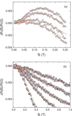
mag-netic field at four temperatures between 0.26 and 4 K. Figure 3共b兲shows the normalized magnetoresistances as a function of magnetic field at five temperatures between 8.5 and 40 K. These figures reveal that the magnetoresistances are negative in all fields at temperatures above ⬃6 K. Nevertheless, be-low 4 K, the magnetoresistances are positive in be-low magnetic fields, changing to negative magnetoresistances in higher magnetic fields. The positive contribution is more pro-nounced at lower temperatures. This marked behavior can be readily understood in terms of the quantum-interference ef-fect in the presence of a notable spin-orbit scattering rate relative to the inelastic electron and electron-phonon scattering rates. Under such conditions, positive magnetoresistances arise owing to the weak-antilocalization effect.4,5
The presence of a notable spin-orbit scattering rate in the ITO-f nanowire can be explained as follows. In this nano-wire, the resistivity 关共共10 K兲=1030 ⍀ cm兲兴 is consider-ably higher than that 共185 ⍀ cm兲 in the ITO-r nanowire.
Therefore, the spin-orbit interaction in this nanowire should be significantly enhanced according to the 共approximate兲 relation:20,33–35 1/
so⬀Z4/e, where Z is the atomic number of the relevant scatterer. A comparatively high resistivity in the ITO-f nanowire implies a relatively short e, which should lead to a large so−1. Quantitatively, we obtain
Lso⬇125 nm in this nanowire 共see below兲. The present
ex-periment suggests that one can tailor both the weak-localization and weak-antiweak-localization effects in ITO nano-wires by carefully controlling the level of atomic imperfections 共point defects and/or heavy impurities兲. This observation provides valuable information about the feasible implementation of future quantum-interference nanodevices. In addition to a long dephasing length 共leading to sensitive quantum transport effects兲, the capability of tuning spin-orbit coupling could be advantageous for the future realization of spintronic devices.36
Our measured magnetoresistances in the ITO-f nanowire can be well described by the predictions of Eq.共1兲 关the solid curves in Figs. 3共a兲 and 3共b兲兴, and the extracted L as a function of temperature is plotted in Fig.4. The inset shows an SEM image of this individual nanowire device. Inspection of Fig. 4 indicates that L in this nanowire is considerably shorter than that in the ITO-r nanowire. This can be ex-plained by the fact that L is suppressed by a high level of disorder, i.e., a short mean-free path, in the ITO-f nanowire. 关Note that Eq. 共3兲 predicts that 1/ee⬀1/
冑
e, and 1/ep⬀1/e in the quasiballistic limit.30,31兴 Our result was fitted to Eq.共2兲 共the solid curve in Fig.4兲 and the adjustable values of 0 and Aep are listed in Table I. Again, we obtain the exponent of temperature p⬇0.69⫾0.12 in ee−1, being very close to the theoretical value of 2/3. In addition, our fitted value of the one-dimensional electron-electron scatter-ing coefficient Aee= 6.4⫻109 K−2/3s−1is in excellent agree-ment with the theoretical prediction of 7.9⫻109 K−2/3s−1 from Eq.共3兲. Such close agreement between experiment and theory most likely arises from the intricate material fact that, though being a doped oxide, ITO possesses a free-carrierlike0.00 0.05 0.10 0.15 0.20 0.25 -0.004 -0.002 0.000 0.002 ∆ R (B )/ R (0 ) B (T) (a) 0.0 0.2 0.4 0.6 0.8 1.0 -0.004 -0.002 0.000 ∆ R (B )/ R (0 ) B (T) (b)
FIG. 3. 共Color online兲 共a兲 Normalized magnetoresistance as a function of perpendicular magnetic field of the ITO-f nanowire at 共form top down兲 0.26, 1.0, 2.0, and 4.0 K. 共b兲 Normalized magne-toresistances as a function of perpendicular magnetic field at共from bottom up兲 8.5, 18, 22, 30, and 40 K. The symbols are the experi-mental data and the solid curves are the theoretical predictions of Eq.共1兲. 0.1 1 10 10 100 L 0 L ϕ (n m ) T (K) 300 40 Lee
FIG. 4. 共Color online兲 Electron dephasing length as a function of temperature for the ITO-f nanowire. The symbols are the experi-mental data and the solid curve is the theoretical prediction of Eq. 共2兲. The extrapolated dashed curve above 12 K is a guide to the eye.
The two straight dashed lines represent our fitted values of L0and
Lee, as indicated. The inset shows an SEM image of this individual nanowire device. The scale bar is 1 m.
共i.e., parabolic兲 electronic band structure.7,12,13 We notice in
passing that, in another high-resistivity nanowire with
d = 110 nm and 共10 K兲=1690 ⍀ cm, we obtained
L共0.25 K兲=170 nm and Lso= 95 nm. These values共scaled for sample resistivities兲 are in good consistency with the cor-responding values in the ITO-f nanowire.
It should be noted that in the ITO-f nanowire, our extracted value of L becomes smaller than the nanowire diameter at a temperature of⬃12 K. That is, a dimension-ality crossover of the weak-localization effect nominally begins to set in at ⬃12 K in this particular nanowire device. Strictly speaking, the measured magnetoresistances should then be least-squares fitted with the three-dimensional weak-localization theoretical predictions5,37 in order to
extract L. However, we found that between 12 and 40 K, our measured magnetoresistances can still be satisfactorily described by Eq. 共1兲 关see Fig. 3共b兲兴 while the three-dimensional weak-localization theory does not apply.38 In any case, the extracted value of L
above 12 K in this nanowire device should be considered only qualitative and treated with caution. 共Hence, in Fig. 4, we only plotted our fitted values of the two contributions L0and
Lee.兲
IV. CONCLUSION
We have quantitatively measured the electron dephasing length in two individual ITO nanowires between 0.25 and 40 K. We observe that the electron dephasing length is very long, reaching 520 nm at 0.25 K in a low-resistivity ITO nanowire. As a consequence, the sample demonstrates strict one-dimensional weak-localization effect up to temperatures above 40 K. In a high-resistivity nanowire, the spin-orbit coupling is enhanced due to a short electron mean-free path, manifesting the weak-antilocalization effect at temperatures below⬃4 K. These observations provide strong indications that robust quantum-interference effects can be realized, and tunable, in ITO nanowires by controlling differing levels of atomic defects and impurities.
ACKNOWLEDGMENTS
The authors are grateful to C. Y. Wu for careful reading of the manuscript, and F. R. Chen and J. J. Kai for providing us with the ITO nanowires used in this study. This work was supported by Taiwan National Science Council through Grant No. NSC 98-2120-M-009-004, and by the MOE ATU Program.
1Y. Imry, Introduction to Mesoscopic Physics共Oxford University Press, Oxford, 1997兲.
2Y. V. Nazarov and Y. M. Blanter, Quantum Transport:
Introduc-tion to Nanoscience共Cambridge University Press, Cambridge,
2009兲.
3S. Washburn and R. A. Webb,Adv. Phys. 35, 375共1986兲. 4B. L. Altshuler, A. G. Aronov, M. E. Gershenson, and Yu. V.
Sharvin, Sov. Sci. Rev., Sect. A 9, 223共1987兲.
5J. J. Lin and J. P. Bird, J. Phys.: Condens. Matter 14, R501
共2002兲.
6Compared with other quantum-interference phenomena, the weak-共anti兲localization method provides the most quantitative way for extracting the electron dephasing time共Refs.5and35兲.
7S. P. Chiu, H. F. Chung, Y. H. Lin, J. J. Kai, F. R. Chen, and J. J. Lin,Nanotechnology 20, 105203共2009兲.
8S. P. Chiu, Y. H. Lin, and J. J. Lin,Nanotechnology 20, 015203
共2009兲.
9Q. Wan, E. N. Dattoli, W. Y. Fung, W. Guo, Y. Chen, X. Pan, and W. Lu,Nano Lett. 6, 2909共2006兲.
10D. Lin, H. Wu, R. Zhang, and W. Pan, Nanotechnology 18,
465301共2007兲.
11C. O’Dwyer, M. Szachowicz, G. Visimberga, V. Lavayen, S. B. Newcomb, and C. M. S. Torres, Nat. Nanotechnol. 4, 239 共2009兲.
12O. N. Mryasov and A. J. Freeman, Phys. Rev. B 64, 233111
共2001兲.
13Z. Q. Li and J. J. Lin,J. Appl. Phys. 96, 5918共2004兲.
14R. B. H. Tahar, T. Ban, Y. Ohya, and Y. Takahashi,J. Appl. Phys. 83, 2631共1998兲.
15A. J. Chiquito, A. J. C. Lanfredi, R. F. M. de Oliveira, L. P. Pozzi, and E. R. Leite,Nano Lett. 7, 1439共2007兲.
16F. Pierre, A. B. Gougam, A. Anthore, H. Pothier, D. Esteve, and N. O. Birge, Phys. Rev. B 68, 085413 共2003兲; Y. Niimi, Y. Baines, T. Capron, D. Mailly, F. Y. Lo, A. D. Wieck, T. Meunier, L. Saminadayar, and C. Bäuerle,ibid. 81, 245306共2010兲. 17While our ITO nanowires are one-dimensional with regard to the
quantum-interference weak-共anti兲localization effect, they are three dimensional with regard to the classical Boltzmann trans-port, i.e., the electron mean-free path l⬍d, the diameter of nano-wire.
18Our Fermi velocities were evaluated by using valus of E
F= 0.7
and 0.4 eV in the ITO-r and ITO-f nanowires, respectively. See Refs.7and13.
19G. Bergmann,Solid State Commun. 42, 815共1982兲.
20P. Santhanam, S. Wind, and D. E. Prober,Phys. Rev. B 35, 3188
共1987兲.
21We note that, in the studies of short nanowires, the effect of measurement-probe geometry on one-dimensional weak-localization magnetoresistance should be treated with caution and may not be always neglected, see V. Chandrasekhar, D. E. Prober, and P. Santhanam,Phys. Rev. Lett. 61, 2253共1988兲. In the present case, the ITO-r nanowire length Lⲏ3Lat the low-est temperatures. The ratio L/L is even larger at higher tem-peratures. In addition, our Cr/Au electrodes were deposited onto the ITO nanowire during separate lithography processes. There were “dirty” interfaces formed between the electrodes and the nanowire. All these factors will render the measuring probe ef-fect less significant. We estimate the efef-fect of measurement-probe geometry, if any exists, would cause a correction of less than a few percent to the present result.
22O. M. Berengue, A. J. C. Lanfredi, L. P. Pozzi, J. F. Q. Rey, E. R. Leite, and A. J. Chiquito,Nanoscale Res. Lett. 4, 921共2009兲.
共2009兲.
24D. Liang, J. Du, and X. P. A. Gao, Phys. Rev. B 81, 153304
共2010兲.
25F. J. Rueß, B. Weber, K. E. J. Goh, O. Klochan, A. R. Hamilton, and M. Y. Simmons,Phys. Rev. B 76, 085403共2007兲.
26J. J. Lin and N. Giordano,Phys. Rev. B 35, 1071共1987兲. 27P. Mohanty, E. M. Q. Jariwala, and R. A. Webb,Phys. Rev. Lett.
78, 3366共1997兲.
28J. J. Lin, T. J. Li, and Y. L. Zhong, J. Phys. Soc. Jpn. 72 共Suppl. A兲, 7 共2003兲.
29S. M. Huang, T. C. Lee, H. Akimoto, K. Kono, and J. J. Lin,
Phys. Rev. Lett. 99, 046601共2007兲.
30A. Sergeev and V. Mitin,Phys. Rev. B 61, 6041共2000兲. 31Y. L. Zhong, A. Sergeev, C. D. Chen, and J. J. Lin,Phys. Rev.
Lett. 104, 206803共2010兲.
32Recent experiment共Ref.9兲 reported that the resistivities of ITO nanowires grown under nominally similar conditions could vary
widely, from⬃100 ⍀ cm to values higher than several thou-sands of microhm centimeter. In our case, the resistivity differs by a much smaller factor of⬍10 共Ref.7兲.
33A. A. Abrikosov and L. P. Gorkov, Zh. Eksp. Teor. Fiz. 42, 1088 共1962兲 关Sov. Phys. JETP 15, 752 共1962兲兴.
34G. Bergmann and C. Horriar-Esser, Phys. Rev. B 31, 1161
共1985兲.
35G. Bergmann,Phys. Rep. 107, 1 共1984兲;Int. J. Mod. Phys. B 24, 2015共2010兲.
36I. Žutić, J. Fabian, and S. Das Sarma,Rev. Mod. Phys. 76, 323
共2004兲.
37C. Y. Wu and J. J. Lin,Phys. Rev. B 50, 385共1994兲.
38Least-squares fits of our measured magnetoresistances with a combined one-dimensional and three-dimensional weak-localization expression did not lead to acceptable values of the adjustable parameters. A weak-localization theory in the cross-over regime is yet to be established.