Optimization of Back Side Cleaning Process to Eliminate
Copper Contamination
Wei-Yang Chou,a,zBing-Yue Tsui,bChia-Wei Kuo,cand Tsung-Kuei Kangd
aInstitute of Electro-Optical Science and Engineering,cDepartment of Physics, National Cheng Kung
University, Tainan 701, Taiwan
bDepartment of Electronics Engineering and Institute of Electronics, National Chiao Tung University,
Hsinchu 300, Taiwan
dDepartment of Electronic Engineering, Feng-Chia University, Taichung, Taiwan
Copper共Cu兲 contamination at the wafer bevel, back side surface, and exclusion zone is identified step-by-step following a typical dual-damascene process. The shield ring of a physical vapor deposition system does not protect the exclusion zone and bevel efficiently. Also, Cu may dissolve and accumulate in the solvent used for post dielectric etch clean. Dissolved Cu atoms may then redeposit on the wafer surface. Furthermore, the rough back side surface traps Cu atoms easier than the smooth front side surface. If there is no SiO2film on the back side surface, post chemical mechanical polish cleaning using dilute HF cannot remove Cu at the back side surface. An optimized single-wafer spin-etch process was proposed. An optimal etchant consisting of HF, HNO3, H2SO4, and H3PO4with ratios 0.5:3:1:0.5 showed excellent performance. Experiments demonstrated that a very short, 10 s, back side clean can totally remove Cu from back side surface, bevel, and 2 mm exclusion zone. A ‘‘wafer shift’’ procedure was also proposed to solve the pinmark issue near the edge pin due to etchant remnant. The optimized cleaning technique shows shorter process time and higher cleaning efficiency than those reported previously.
© 2005 The Electrochemical Society. 关DOI: 10.1149/1.1850381兴 All rights reserved.
Manuscript submitted May 25, 2004; revised manuscript received July 14, 2004. Available electronically January 5, 2005.
With the progress of integrated circuit共IC兲 processing technol-ogy, the feature size is scaled down continuously. As the device performance and the circuit density are improved due to shorter channel length and smaller device geometry, the resistance and ca-pacitance of multilevel interconnects are increased due to the thinner and longer metal wires and the narrower space between them. Cop-per 共Cu兲 has been recognized as the most suitable alternative for aluminum as an interconnect material because of its low electrical resistivity and excellent electromigration resistance.1,2However, Cu is a fast diffuser in both silicon and silicon dioxide.3-5Copper con-tamination in the dielectric results in device instability and degrada-tion of dielectric reliability.6-12Also, Cu in the silicon serves as a defect center to kill minority carrier lifetime and to increase junction leakage current.13-17Much effort has been devoted to controlling Cu contamination at front side wafer surfaces. Low power dielectric etching, high efficiency cleaning solutions, and reliable diffusion barriers have been developed. Although it was reported that Cu con-tamination at the back side surface of wafers cannot diffuse to the front surface of wafers under the thermal budget of the backend of line 共BEOL兲,18 apparent Cu migration from back side surface to front surface has been observed under the thermal budget of fron-tend of line共FEOL兲 processing.19Furthermore, cross contamination through direct contact to the contaminated bevel and back side sur-face of wafers during wafer transfer and handling is still a major issue in manufacturing.
The dual damascene process is well accepted for Cu intercon-nects, due to the difficulty in plasma etching Cu films. After the first Cu-interconnect layer is completed, the intermetal dielectric共IMD兲 is deposited as the next layer in a typical Cu dual damascene pro-cess. The sequential photolithography process and dielectric etching processes are performed twice to form the via holes and trenches in the IMD. After premetal deposition cleaning, the barrier metal and Cu are then deposited in the via holes and trenches. Generally, Cu deposition is performed with two steps: a seed layer deposited by physical vapor deposition 共PVD兲 and a main layer deposition by electroplating. A chemical mechanical polishing共CMP兲 process is performed to finish the second layer Cu-interconnect. There are many opportunities for Cu to be exposed to the process environment or for wafers to be exposed to a Cu contaminated environment. For example, after IMD patterning, Cu at the via bottom is exposed to
the postetch cleaning environment. Also, the wafer back side surface may contact with a solution containing copper during CMP.
The increased use of copper in semiconductor industries creates the problem of Cu cross contamination from one wafer to another via handling tools which handle wafers only at the wafer edge to avoid damaging the active devices fabricated on the wafer front side. Copper must be eliminated from each wafer back side surface, bevel edge, and front side exclusion zone to prevent contamination of subsequent wafers being processed. Therefore, it is important to clean the wafer bevel and back side surface after every process step that may expose the wafer to copper contamination. A single-wafer cleaning technology, known as spin-process contamination elimina-tion (SpCE), was proposed to reduce Cu contamination.20-23 How-ever, the process conditions and chemicals are not optimized. Fur-thermore, the acid remnant problem at the wafer edge where perimeter pins contact the wafer damages the device on the front side of the wafer. Traditionally, the method to solve the acid remnant problem is to provide an undercut rinse共UCR兲 module in the clean-ing equipment or to add a process step of deionized共DI兲 water rinse on the front side of wafer after cleaning the back side. However, the stability of the UCR module is still questionable and the DI water rinse increases process time.
In this work, Cu contamination at the wafer bevel and back side surface was investigated at each step in the typical dual-damascene process. The results are presented and discussed in the next section. The structure and operation principle of the cleaning equipment used in this work are explained later. A newly developed chemistry was used to remove Cu from the wafer back side, bevel edge, and front edge exclusion zone. A simple wafer-shift scheme was pro-posed to efficiently eliminate the deleterious effects of acid remnants at the perimeter pins centering the wafer. The detailed process con-ditions and experimental results are discussed last. Finally, by adopt-ing this optimized cleanadopt-ing process in the BEOL process, we dem-onstrate that the yield of product with Cu interconnect can be as high as that with Al interconnect.
Cu Contamination during Processes
Cu contamination during postetch clean.—After IMD etching to form a dual-damascene structure, wafers are typically cleaned with solvents in a wet bench to remove polymer residues and Cu contain-ing compounds on the sidewall and bottom of the damascene struc-ture. Cu dissolves in the solvent and then the Cu content in it in-creases with increasing process time. In this subsection, we examine whether Cu in the solvent will redeposit on wafer surface. zE-mail: weiyang@mail.ncku.edu.tw
In this experiment, a widely used solvent for the Cu process, ACT-970, was used. The typical process condition is at 80°C for 20 min. The etching rate of copper in ACT-970 is 2.17 Å/min at 80°C. Before the experiment, the wet bench was flushed with DI water and all filters were replaced with new filters. The process tank was then filled with fresh solvent. Approximately 100 mL of solvent was sampled from the tank before the process. To increase Cu in the solvent, 25 wafers共diameter 200 mm兲 with a blanket Cu film of 200 nm were processed with the standard postetch clean recipe eight times. Again, approximately 100 mL of solvent was sampled from the tank. The Cu content in fresh as well as processed solvents was analyzed by inductively coupled plasma mass spectrometry 共ICP-MS兲. A similar sampling procedure was performed once again after the wet bench was in normal operating conditions for three months. DI water flushing and filter replacement were not done during this three month period, but the solvent was drained and replenished with fresh solvent every 2-3 days. The fresh solvent was also sampled. 25 200 mm wafers with a 200 nm blanket Cu film were processed with the standard postetch clean recipe eight times. Again, approximately 100 mL of the solvent was sampled from the tank. The original Cu content is lower than 1 ppb. After eight continuous runs with the copper-coated wafers, the Cu content increased dra-matically to 2483 ppb. The Cu content in the tank accumulates with increasing process time. After three months, even if fresh solvent was fed into tank, the Cu content was as high as 245 ppb. Once again, the Cu content increased to 2650 ppb after eight continuous runs of copper-coated wafers at this time.
A bare Si wafer and a blanket undoped silica glass 共USG兲/Si wafer were processed with the standard postetch clean recipe imme-diately after the eight continuous runs of blanket Cu wafers. The
concentrations of Cu on the front side as well as back side surfaces of bare Si wafer and on the front side surface of USG/Si wafers were analyzed by vapor-phase decomposition ICP-MS 共VPD-ICP-MS兲 and were 1.25⫻ 1010, 5.76⫻ 1012, and 0.89 ⫻ 1010
atom/cm2, respectively. The detection limit for Cu is 109atom/cm2. Cu does not redeposit on the front side surface of a wafer regardless whether the surface material is Si or SiO2. A very high surface concentration of Cu was observed on the back side surface of bare Si wafer. Possibly, Cu atoms were trapped in the valleys of the rough back side surface of the wafer.
The proceeding experiment indicates that Cu atoms may accu-mulate in the solvent and process tank. It also shows that they can redeposit on wafer rough surfaces. The DI water should be flushed periodically and filters should be replaced to maintain the wet bench for processing. Also, a suitable back side cleaning is strongly rec-ommended to reduce the risk of Cu redeposition.
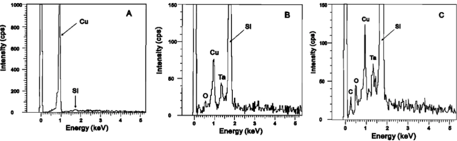
Cu contamination during Cu deposition.—A 1m SiO2film was thermally grown on a 200 mm Si wafer. A 100 nm tantalum layer was deposited in a PVD system with no shield ring at the wafer edge. Then a 1 m Cu film was deposited in a long-throw PVD system with a shield ring at the wafer edge. The gap between wafer surface and shield ring was approximately 1 mm and the exclusion zone was approximately 3 mm in width from the edge of the wafer. Optical microscope inspection showed a clear boundary for the exclusion zone. However, energy dispersion spectroscopy 共EDS兲 analysis in a scanning electron microscope共SEM兲 system performed at the exclusion zone detected a strong Cu signal. Figure 1 illustrates the positions where the EDS analyses were performed. Position A is near the boundary of exclusion zone, position B is at the midpoint of the exclusion zone, and position C is at the wafer bevel. Figure 2a-c shows the EDS spectra at position A, B, and C, respectively. A strong Cu signal is still detected even at the wafer bevel. Clearly the shield ring does not effectively prevent Cu deposition in the exclu-sion zone. Therefore, a suitable cleaning process to remove Cu in the exclusion zone and at the wafer bevel is necessary.
Cu contamination during CMP.—During CMP, wafers are im-mersed in a solution containing Cu. Copper particles and dissolved Cu atoms may redeposit not only on the wafer front surface but also on the back side and on the bevel. The typical post Cu CMP clean-ing method is a double-side cleanclean-ing with dilute HF共DHF兲 solution. The wafer structure used in this experiment is Cu共200 nm兲/USG 共1 m兲/Si. The 1 m USG film was deposited in a plasma-enhanced chemical vapor deposition共PECVD兲 system and the 200 nm Cu film was deposited in a PVD system. The Cu film was removed by stan-dard Cu CMP process followed by post-CMP cleaning process using DHF. Wafers 1 and 2 received the CMP and post-CMP cleaning processes one time. The other three wafers共3-5兲 received the CMP and post-CMP cleaning processes two times. The CMP process
re-Figure 1. Three measurement positions where EDS analysis was performed.
共A兲 Nearby the edge of exclusion zone 共about 3 mm away from wafer edge兲, 共B兲 midway of exclusion zone, and 共C兲 at wafer bevel.
moved 20 and 50 nm USG at the first and second CMP processes, respectively. The surface concentration of Cu at the back side and front side of wafers was then analyzed by total reflective X-ray fluorescence spectroscopy共TXRF兲. The detection limit for Cu was 1010atom/cm2. Five positions were measured on each wafer. The positions of the five measurement points are shown in Fig. 3.
Table 1 lists the split conditions and results of this experiment. When the wafers were processed by CMP once共wafers 1 and 2兲, copper contamination on the back side surface of wafers was below the detection limit of TXRF. For the wafers that received the CMP process twice, severe Cu contamination was observed at the wafer back side surface共wafers 3 and 4兲 but no Cu contamination on the front side surface共wafer 5兲. Because DHF was used for post-CMP cleaning, a thin SiO2 layer of about 10 nm on the front side was etched away. It is an efficient method to remove contamination on or embedded in SiO2. Thus, even if the wafers received the CMP process several times, no Cu signal was detected on the front side after post-CMP cleaning. There was a thin native SiO2layer at the back side originally. Before post-CMP the back side surface was hydrophilic because of a large amount of Si-O bonds on it. The first post-CMP clean etched this copper contaminated surface oxide layer, which explains the high efficiency of post-CMP cleaning on back surface of the wafers that received the Cu CMP once. After
post-CMP treatment, Si-H bonds appeared on the back side surface at about a monolayer density. For wafers that received the Cu CMP process twice, the property of back side surface was hydrophobic due to Si-H bonds on the back side surface; hence the post-CMP cleaning efficiency became relatively weak. If the copper adheres to the back side, the silicon and copper may not be etched by the post-CMP echant.24,25
This study indicates that the efficiency of post-CMP cleaning depends on the properties of wafer surface. If Si-H bonds appear on wafer surface during the post-CMP clean, it is possible for Cu atoms to remain on the wafer surface.
Equipment Description
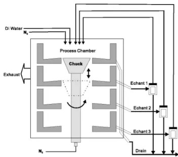
As described in the previous section, Cu contamination may oc-cur at the wafer back side, bevel edge, and front surface exclusion zone. Such Cu contamination must be removed entirely to prevent cross contamination and subsequent processing problems. A single-wafer spin-etch equipment with a Bernoulli chuck was used for this purpose.
As shown in Fig. 4, the core of the equipment is a single wafer process chamber within which the wafer is supported on the Ber-noulli chuck. The wafer is supported, with the front side down and back side up, on a nitrogen gas blanket created by controlled nitro-gen flow through the chuck. Six perimeter pins共not shown in Fig. 4兲 are in contact with the wafer edge to center the wafer within the process chamber. A pipe vents gases, e.g., nitrogen from the wafer chuck, from the process chamber. The wafer is spun with the chuck and perimeter pins. Supply lines from media tanks supply the se-lected media, or chemicals/solutions to the process chamber and terminate at radially oscillating overhead nozzles spaced apart from the wafer. An etchant, for example, is dispensed from an overhead nozzle onto the back side of wafer. Control of etchant viscosity, simultaneous radial and tangential etchant flow, and Bernoulli gas flow enables etching of Cu contamination from the wafer back side. A ‘‘wraparound’’ effect also permits removal of thin-film contami-nation from the bevel and front side exclusion zone from 0.5 to 5.0 mm of the wafer edge.
The process chamber includes stacked process levels, which re-ceive the specific chemicals applied to the spinning wafer from the respective media supply lines. The wafer is raised or lowered with the chuck and perimeter pins to level with the stacked process level corresponding to the chemical to be applied to the wafer. The chemi-cals are collected and removed from the process chamber via
respec-Figure 3. Five measurement positions where the TXRF analysis was
per-formed.
Figure 4. Schematic cross-sectional illustration of the process chamber of
the single-wafer spin-etch equipment used in this work.
Table I. Cu contamination at wafer back side surface or front side surface after Cu-CMP and post-CMP cleaning with DHF.
Wafer ID Structure
Cu-CMP 共times兲 TXRF
Average Cu concentration (1010atom/cm2) 1 Cu/SiO2/Si 1 Back side Below detection limit 2 Cu/SiO2/Si 1 Back side Below detection limit
3 Cu/SiO2/Si 2 Back side 11-67
4 Cu/SiO2/Si 2 Back side 18-104
tive media return lines. The collected chemicals can be filtered, re-turned to the media tanks, and reused. If the contamination from recirculated chemicals is a concern, the used chemical can be drained directly. The above process avoids the necessity of having to protect the front side of the wafer from the etchant. For example, the etchant is selectively applied to the back side of a spinning wafer and spun off the wafer into the selected process level. After the etching or cleaning step, the wafer is then repositioned adjacent to another corresponding process level and is then cleaned or rinsed with DI water and then rapidly dried with a flow of nitrogen.
Optimized Cleaning Process
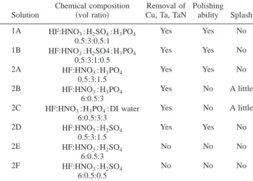
Etchant selection.—To etch away a thin surface layer one must remove Cu contamination completely. Furthermore, a smooth sur-face is preferred to avoid trapping of Cu atoms. Thus, an acceptable Cu-clean recipe must satisfy several requirements including good uniformity, suitable viscosity to clean the bevel and exclusion zone, the ability to etch several thin films such as Si, SiO2, Ta, and TaN, and the ability to polish the back side of the wafer.
First a suitable etchant composition was developed. Etchants with various compositions from the four acids; HF, HNO3, H2SO4, and H3PO4were mixed and the basic performance was evaluated. The role of nitric acid was to eliminate Cu contamination and oxi-dize the silicon on the back surface of wafer.21 HNO3 can also oxidize most metals to the corresponding cation. Hydrofluoric acid was used to remove silicon dioxide from the back side or bevel of the wafer and also the barrier film of Ta or TaN at the bevel or exclusion zone of the wafer. The etch rate of Si and SiO2 may be adjusted by altering the content of HF and HNO3 in the etchant. Phosphoric acid and sulfuric acid were used to polish the silicon surface to reduce the trapping of metal atoms in the subsequent process.
Two sets of four acid etchants consisted of HF, HNO3, H2SO4, and H3PO4, three sets of three acid etchants consisted of HF, HNO3, and H3PO4, and another three sets of three acid etchants consisted of HF, HNO3, and H2SO4. These etchants were prepared for cleaning processes and all are listed in Table II. Two acid etchants consisting of only HF and HNO3were also evaluated. The etch rate of Si and SiO2and the polishing ability was much poorer than those of the three acid and four acid etchant mixtures.
Table II shows the eight etchant mixtures in which the etching ability of Cu共1 m兲/Ta or TaN 共500 Å兲 film grown on the silicon wafer, the polishing ability on the wafer back side surface, and the splash phenomenon at perimeter pins are also listed. Etchants 2E and 2F cannot remove the Cu共1 m兲/Ta or TaN 共500 Å兲 film
com-pletely within the 60 s processing time, because these etchants have very low etch rates for Ta and TaN films. Etchants 2B, 2C, 2E, and 2F with high ratio of HF can not polish the back surface of the wafer because the etch rate of silicon dioxide is too high. A high amount of acid accumulated near the pin splashes onto the wafer front side when the back side cleaning process is performed. The splash phe-nomenon depends on the viscosity of the etchant mixture. Splashing at the perimeter pins may occur due to increasing the ratio of HF or adding DI water.
The polishing ability can be judged qualitatively by inspecting the surface reflectivity. The polishing ability strongly depends on the ratio of HF and HNO3. For a high HF/HNO3 ratio, the polishing ability was diminished. H2SO4 and H3PO4 play a similar role on polishing ability. Among the eight etchants, only four etchants, 1A, 1B, 2A, and 2D, have the ability to polish Si. Microroughness mea-surements were performed on the back side surface of a bare silicon wafer using a contact mode atomic force microscope共AFM兲 before and after a wafer processed with the 1B or 2B etchant for 60 s. Figure 5a, b, and c shows the morphology states before and after processing with etchants 1B and 2B, respectively. The
root-mean-Figure 5. Three-dimensional maps of microroughness of the back side
sur-face of wafers共a兲 before back side cleaning process, 共b兲 after cleaning with the 1B etchant for 60 s, and共c兲 after cleaning with the 2B etchant for 60 s.
Table II. Chemical compositions of etchants and the correspond-ing process properties.
Solution
Chemical composition
共vol ratio兲 Cu, Ta, TaNRemoval of
Polishing ability Splash 1A HF:HNO3:H2SO4:H3PO4 0.5:3:0.5:1 Yes Yes No 1B HF:HNO3:H2SO4:H3PO4 0.5:3:1:0.5 Yes Yes No 2A HF:HNO3:H3PO4 0.5:3:1.5 Yes Yes No 2B HF:HNO3:H3PO4 6:0.5:3 Yes No A little 2C HF:HNO3:H3PO4:DI water
6:0.5:3:3 Yes No A little 2D HF:HNO3:H2SO4 0.5:3:1.5 Yes Yes No 2E HF:HNO3:H2SO4 6:0.5:3 No No No 2F HF:HNO3:H2SO4 6:0.5:0.5 No No No
square 共rms兲 roughness of the initial wafer was 0.177 m. After processing with the 1B etchant, the rms roughness decreased to 0.104m. When processed with the 2B etchants, the rms roughness increased to 0.208m. Apparently the high HF content degrades the polishing ability.
Table III lists the etch rate uniformity of 1A, 1B, 2A, and 2D etchants. Because the etch rate of bare Si is difficult to measure, the etch rate of SiO2was measured instead. The etch rate for the four etchant mixtures were similar, but the 1B etchant showed the best etching rate uniformity.
According to the above results, the 1B etchant showed the best uniformity, good polishing ability of Si surface, good ability to etch Cu, Ta, and TaN, and no splash problem at the perimeter pins. Therefore, the 1B etchant was employed in the following subsec-tions to further optimize the cleaning techniques.
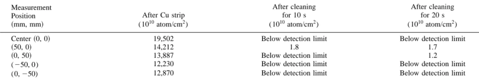
Back side clean.—To evaluate the efficiency of the back side cleaning with the four acid mixture, the cleaning process with etchant 1B was performed on wafers that had a 2000 Å thick copper layer deposited directly on bare silicon. The copper film was stripped using an etchant consisting of H3PO4and HNO3in a vol-ume ratio of 2:0.12 at 45°C. The etch rate of etchant 1B was mea-sured on a photoresist patterned wafer. After etching with etchant 1B for 10 and 20 s and removal of photoresist, the thicknesses of Si removed were measured with a surface profiler and were 260 and 530 nm, respectively. The copper concentration on the wafer surface before and after cleaning was analyzed with TXRF. Table IV lists the measurement results. A very high surface concentration of Cu, higher than 1⫻ 1014atom/cm2, was detected on the Si surface after stripping of Cu film. This result indicates that even without thermal treatment, Cu atoms are still interacted with Si or diffused into it to a shallow depth. A 10 s cleaning with etchant 1B was sufficient to reduce the surface concentration of Cu to 1⫻ 1010atom/cm2 or below. This is far below the failure threshold of 5.0 ⫻ 1010atom/cm2for copper at BEOL processes.21,26-28The process time used in this work is shorter than that reported by Itoh et al.23 and the efficiency of cleaning is also better.
Bevel and exclusion zone clean.—Cu was deposited on the wafer bevel and exclusion zone during the PVD process step. It is prefer-able to clean the bevel and exclusion zone simultaneously with the back side surface in the same process step. During the back side clean, the etchant removed approximately 200 nm of Si from the back surface of the wafer so that any Cu contamination within the Si surface layer was removed. A ‘‘wraparound effect’’ permited the
removal of the thin film at the beveled edge and the front side exclusion zone. The width of exclusion zone that can be cleaned depended on the viscosity of etchant, the spin speed, and the nitro-gen flow rate of the Bernoulli chuck. The exclusion zone resulted from the photolithography process and was variable. Typically it was 2 mm for the current deep submicrometer process technology. Therefore, it is satisfactory to clean the wafer bevel edge and front side exclusion zone of 1 to 2 mm when the wafer back side is cleaned.
To evaluate the cleaning ability at the wafer bevel and exclusion zone, wafers with Cu共200 nm兲/SiO2共1 m兲/Si were prepared. No shield ring was used during the Cu deposition. Therefore, the exclu-sion zone and wafer bevel were covered with Cu film. With a chuck spin speed from about 175 to 300 rpm and a nitrogen chuck flow rate from about 70 to 300 L/min, the exclusion zone can be cleaned from 2 to 1 mm, respectively. This result is similar to that reported in Ref. 23. Figure 6 shows the EDS spectra on the front side of wafer at the position of 2 and 2.5 mm away from the wafer edge after cleaning at a chuck spin speed of 175 rpm and a chuck nitrogen flow rate of 70 L/min for 10 s. Clearly, within the 2 mm exclusion zone, all the Cu can be removed using the above cleaning recipe.
Pinmarks.—Although no splash problem was encountered in the above experiments, it was observed that the etchant, i.e., acid solu-tion, accumulated near the perimeter pins at the wafer edge and corroded the Cu film around the perimeter pins gradually forming a pinmark. Figure 7 shows an example of the pinmark. The process parameters must be further optimized to solve this problem. In this work, a ‘‘wafer shift’’ technique is proposed to solve the pinmark problem.
Figure 6. EDS spectra on the front side of wafer at the position of共a兲 2 mm
共solid line兲 and 共b兲 2.5 mm 共dashed line兲 away from wafer edge after clean-ing at a chuck spin speed of 175 rpm and a chuck nitrogen flow rate of 70 L/min for 10 s.
Table III. Etching rate and uniformity of the etchants that can polish the wafer back side surface.
Solution
Etching rate for SiO2
共nm/min兲 Uniformity 共3兲 共%兲 1A 149 3.7 1B 148 2.9 2A 144 5.2 2D 144 4.7
Table IV. Cu concentration on wafer back side surface after cleaning it with the 1B etchant for 10 and 20 s.
Measurement Position
共mm, mm兲 (10After Cu strip10atom/cm2)
After cleaning for 10 s (1010atom/cm2) After cleaning for 20 s (1010atom/cm2)
Center共0, 0兲 19,502 Below detection limit Below detection limit
共50, 0兲 14,212 1.8 1.7
共0, 50兲 13,887 Below detection limit 1.2
(⫺50, 0) 12,230 Below detection limit Below detection limit
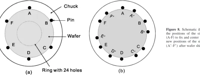
As shown in Fig. 8a, nitrogen gas flows through the Bernoulli chuck in a predetermined pattern and supports the wafer back side on a cushion of nitrogen gas. In this work, the chuck has 24 holes through which nitrogen flows to support the wafer initially and then six perimeter pins contact the wafer edge共labeled A-F兲 to fix the wafer position. At a predetermined time, the etchant flow was stopped and wafer was rotated relative to the chuck so that the contact positions A-F were shifted to A⬘-F⬘ as shown in Fig. 8b. Specifically, the rotation speed of chuck was accelerated so that the rotation speed of pins was greater than the rotation speed of the wafer. Nitrogen flow through the chuck was maintained. At the point of wafer shift, the perimeter pins released briefly to avoid acid ac-cumulation at pin locations A-F and the pins then recontacted the wafer at A⬘-F⬘. This process was repeated at predetermined
inter-vals. This washed away any accumulation of the etchant in the prox-imity of contacts A-F. At the next and any subsequent wafer shifts, contact positions A⬘-F⬘are changed to A⬙-F⬙, and contact positions A⬙-F⬙are subsequently changed to contacts A-Fand so on. The wafer shift procedure was continuously performed throughout the clean step and the DI water rinse step.
Based on the above concept, the back side clean recipe used in the previous section was modified by incorporating the wafer shift procedure. The etchant was applied to the wafer for a total time of 10 s. The wafer shift function was done every 3 s, that is the wafer shift occurred around the third and sixth second of the 10 s cleaning step. Once the cleaning step was completed, the wafer was shifted again and DI water was applied to rinse the wafer. During the 30 s rinsing step, the wafer was shifted about every 10 or 15 s with a DI water flow rate of 1-2 L/min. With the wafer shift operation, the pinmark totally disappeared.
Product Verification
The optimized cleaning technique has been integrated into the multilevel interconnect process. The back side of the wafer is cleaned after every process step of Cu deposition, IMD postetch cleaning, and post-CMP cleaning. A test vehicle with one poly-Si layer and three Al-interconnect layers was used to verify the clean-ing technique. There are six test circuits in the test vehicle: Two logic circuits and four static random access memory共SRAM兲 cir-cuits. Wafers were processed to the formation of W-contact plug. Four wafers were fabricated with the conventional Al-interconnect process and the other four wafers were fabricated with the Cu-interconnect process. The first Cu layer was formed with a single-damascene process and the other layers were formed with a dual-damascene process. 97 dies were measured on each wafer. Figure 9
Figure 7. Optical microscopic image of pinmark at wafer edge proximate to
the perimeter pins.
Figure 8. Schematic illustrations of 共a兲
the positions of the six perimeter pins 共A-F兲 to fix and center wafer and 共b兲 the new positions of the six perimeter pins (A⬘-F⬘) after wafer shift.
Figure 9. The yield of the six test circuits with Cu interconnect. The results
shows the average yield of Cu-interconnect wafers normalized to the yield of Al-interconnect wafers. The yields of the six test circuits were almost identical.
Conclusions
Copper contamination of the wafer bevel, back side surface, and exclusion zone were identified step-by-step for the dual-damascene process. It was observed that the shield ring of the PVD system did not protect the exclusion zone and wafer bevel from Cu contamina-tion efficiently. It was also observed that Cu may dissolve and ac-cumulate in the solvent used for post-IMD etch clean and the dis-solved Cu atoms may redeposit on the back side surface due to the surface roughness. Once Cu atoms are deposited on the wafer sur-face, a simple surface cleaning is not able to remove them entirely. The most efficient method to remove Cu totally is to etch away the thin oxide surface layer. It was also shown that the rough back side surface more easily trapped Cu atoms than the smooth front surface. The back side surface polished wafer is not sensitive to Cu contami-nation. In that there is no SiO2on the back side surface, post-CMP cleaning using dilute HF is unable to remove Cu from the back side surface.
To ensure that the wafer bevel, back side surface, and exclusion zone are free of Cu contamination, an optimized single-wafer spin clean process was developed. Several etchants, mixtures of four ac-ids, three acac-ids, and two acac-ids, were prepared and examined. An etchant consisting of HF, HNO3, H2SO4, and H3PO4 with ratios 0.5:3:1:0.5 showed the best uniformity, good polishing ability for the back side surface, good etching ability of Cu, Ta, and TaN, and no splash problem at the perimeter pins. Experiments demonstrated that a very short 10 s back side cleaning can totally remove Cu from the back side surface, bevel, and 2 mm exclusion zone. A wafer shift procedure was also proposed to solve the issue of pinmarks at the edge pins due to etchant accumulation. The optimized cleaning dem-onstrated shorter process time and higher cleaning efficiency than processes reported previously. Finally, a test vehicle with six types of circuits demonstrated identical yield of wafers fabricated with Al-interconnect and Cu-interconnect.
It is concluded that with a suitable back side cleaning process, wafers with no Cu contamination at the wafer bevel, back side, and exclusion zone can be guaranteed. A low cost, high throughput, high efficiency back side cleaning technique was demonstrated using a single-wafer spin clean equipment with a Bernoulli chuck. With this optimized cleaning technique, cross contamination during the Cu process during wafer handling and wafer transfer can be eliminated.
Acknowledgment
The authors thank everybody in the deep sub-micron technology division, ERSO/ITRI involved in wafer processing, electrical mea-surement, and contamination monitoring; and further thank the Na-tional Science Council of Taiwan for financially supporting this re-search under contract no. NSC92-2112-M-006-018. We are also grateful to Professor Gwo at the Department of Physics, National
Tsing Hua University for his help with AFM measurement. The Macronix International Co. Ltd., Taiwan, provided the test vehicle. National Cheng Kung University assisted in meeting the publication costs of this article.
References
1. S. P. Muraka, R. J. Gutmann, A. E. Kaloyeros, and W. A. Lanford, Thin Solid
Films, 236, 257共1993兲.
2. D. Edelstein, J. Heidenreich, R. Goldblatt, W. Cote, C. Uzoh, N. Lustig, P. Roper, T. McDevitt, W. Motsiff, A. Simon, J. Dukovic, R. Wachnik, H. Rathore, R. Schulz, L. Su, S. Luce, and J. Slattery, in Tech. Dig. - Int. Electron Devices Meet., 1997, 773.
3. R. N. Hall and J. H. Racette, J. Appl. Phys., 35, 379共1964兲.
4. J. D. McBrayer, R. M. Swanson, and T. W. Sigmon, J. Electrochem. Soc., 133, 1242共1986兲.
5. Y. J. Kim, K. K. Choi, and O. Kim, IEEE Electron Device Lett., 23, 479共2002兲. 6. K. Hiramoto, M. Sano, S. Sadamitsu, and N. Fujino, Jpn. J. Appl. Phys., Part 2, 28,
L2109共1989兲.
7. A. L. S. Loke, J. T. Wetzel, P. H. Townsend, T. Tanabe, R. N. Vrtis, M. P. Zussman, D. Kumar, C. Ryu, and S. S. Wong, IEEE Trans. Electron Devices, 46, 2178
共1999兲.
8. M. Inohara, H. Sakurai, T. Yamaguchi, H. Tomita, T. Iijima, H. Oyamatsu, T. nakayama, H. Yoshimura, and Y. Toyoshima, in Proceedings of the 2000
Sympo-sium VLSI Technology, p. 26共2000兲.
9. A. Mallikarjunan, S. P. Murarka, and T. M. Lu, Appl. Phys. Lett., 79, 1855共2001兲. 10. K. L. Fang and B. Y. Tsui, J. Appl. Phys., 93, 5546共2003兲.
11. C. C. Chiang, M. C. Chen, Z. C. Wu, L. J. Li, S. M. Jang, C. H. Yu, and M. S. Liang, J. Electrochem. Soc., 151, G89共2004兲.
12. T. K. Kang and W. Y. Chou, J. Electrochem. Soc., 151, G391共2004兲.
13. C. Ahrens, D. Depta, F. Schitthelm, and S. Wilhelm, Appl. Surf. Sci., 91, 285
共1995兲.
14. B. Vermeire, L. Lee, and H. G. Parks, IEEE Trans. Semicond. Manuf., 11, 232
共1998兲.
15. K. S. Low, M. Schwerd, H. Koerner, H. J. Barth, and A. O’Neill, in Proceedings of
the SPIE 1999 Symposium and Continuing Education Program Microelectronic Manufacturing, p. 24共1999兲.
16. K. Hozawa, H. Miyazaki, and J. Yugami, Tech. Dig. - Int. Electron Devices Meet., 2002, 737.
17. Y. J. Kim and O. Kim, in Digest of Microprocesses and Nanotechnology
Confer-ence, p. 126共2002兲.
18. K. C. Tee, K. Prasad, C. S. Lee, H. Gone, C. L. Cha, L. Chan, and A. K. See, IEEE
Trans. Semicond. Manuf., 14, 170共2001兲.
19. K. Hozawa, T. Itogo, S. Isomae, and M. Ohkura, in Proceedings 1999 Symposium
on VLSI Technology, p. 129共1999兲.
20. P. S. Lysaght and M. West, Solid State Technol., 1999, 63共Nov兲.
21. P. S. Lysaght, I. Ybarra, T. Doros, J. V. Beach, H. Sax, J. L. Mello, M. G. West, and G. Gupta, in Cleaning Technology in Semiconductor Device Manufacturing VI, T. Hattori, R. E. Novak, and J. Ruzyllo, Editors, PV99-36, p. 343, The Electrochemi-cal Society Proceedings Series, Pennington, NJ共1999兲.
22. E. Gaulhofer, H. Oyrer, and B. Y. Tsui, in Semiconductor Fabtech, 11th ed., p. 289
共2000兲.
23. M. Itoh, Y. Ishii, T. Jinbo, H. Akimori, T. Futase, and T. Saeki, IEEE Trans.
Semicond. Manuf., 13, 300共2000兲.
24. T. Takahagi, I. Nagai, A. Ishitani, H. Huroda, and Y. Nagasawa, J. Appl. Phys., 64, 3516共1988兲.
25. N. Hirashita, M. Kinoshita, I. Aikawa, and T. Ajioka, Appl. Phys. Lett., 56, 451
共1990兲.
26. N. Awaya, H. Inokawa, E. Yamamoto, Y. Okazaki, M. Miyake, Y. Arita, and T. Kobayashi, IEEE Trans. Electron Devices, 43, 1206共1996兲.
27. H. Miyazaki, H. Kojima, and K. Hinode, J. Appl. Phys., 81, 7746共1997兲. 28. B. Vermeire, C. A. Peterson, H. G. Parks, and D. Sarid, in IEEE 37th Annual