~
332 IEEE TRANSACTIONS ON CIRCUITS AND SYSTEMS FOR VIDEO TECHNOLOGY, VOL. 5, NO. 4, AUGUST 1995
Scalable Array Architecture Design
for Full Search Block Matching
Shifan
Chang,
Juin-HaurHwang,
and Chein-Wei Jen, Member, IEEEAbstract-Block matching is a widely used motion estimation algorithm in current video systems. Among typical searching strategies, the full search scheme provides better precision and regular data flow as well as higher parallelism, a character- istic that is advantageous for VLSI implementation. However, the huge computation load incurred by full search results in high cost, especially in high pixel rate applications. Since block matching algorithm is used in a wide range of pixel rates, an architecture that is cascadable and offers variable computing power is promising. In the first part of this paper, an approach based on dependence graph (DG) is proposed to analyze the operation sequence and data flow of full search block match- ing. The approach employs a transformation on DG’s, called slice and tile, to produce different forms of DG’s. Through this technique, most existing architectures can be represented in graphs for analysis, and new architectures can be found. In the second part of this paper, a new architecture is presented that features cascadable modules of processing elements (PE’s) with simple interconnection. Therefore, flexibility in computing power is available. The other advantages include variable sizes of the search area and 100% PE utilization. These characteristics offer great flexibility and efficiency for different applications. This architecture is implemented with thirty-two PE’s in one chip that consists of 102 K transistors.
I. INTRODUCTION
LOCK MATCHING is widely adopted in video applica-
B
tions to identify redundancy between frames. An image frame is partitioned into equal-sized template blocks, and for each template block, a similar block is found among the candidate blocks in a search area located in some other frame. The position of the similar block in the search area is called motion vector, which is the target of block matching because the motion vector can be used to find the similar block and reconstruct the image. The measure of closeness between the template block and the similar block can be sum of absolute difference (SAD), mean square error, pel-difference classification [l], minimax [ 2 ] , etc. In this paper, SAD is assumed, but other measures that are based on pixel-to-pixel operations are also implied.To find a similar block, a better approach is to check all the candidate blocks in the search area. This approach, called full search block matching (FSBM), can be formulated as follows:
Manuscript received February 3, 1994; revised December 21, 1994. This
work was supported by National Science Council under Grant NSC81-0404- EOO9-134. This paper was recommended by Associate Editor P. Pirsch.
The authors are with the Department of Electronics Engineering and Institute of Electronics, National Chiao Tung University, Hsinchu 300 Taiwan,
R.O.C.
IEEE Log Number 9414224.
Y
0 1 2 3 4 s
(k,l)= position of (0.0) of template block on search area Fig. 1. Template block and search area. N = A- = 4.
Let Block size = N x N Tracking range =
K
xK
c ( m , n ) : template block m = ( K + N - l ) x ( K - ) p ( z , y): search areamv(k, 2): index of position IC, 2 = 0 . .
.
( K - 1)z, y = 0 . .
.
( K
+
N
- 2) N-1 N-1m=O n=O
The motion vector is
(L,i)
that produces the smallest SAD(k,Z). Fig. 1 shows a typical template block and the corresponding search area withN
=K
= 4. The template block can be placed over the search area and moves four positions both horizontally and vertically. Compared with some simplified algorithms [3]-[6], FSBM also provides regular operatioddata sequences, which is advantageous for VLSI implementation. However, the large amount of computation and the high input bandwidth are the challenges in realization, especially for high pixel rate applications.Many hardware realizations of FSBM have been proposed. However, for higher pixel rate applications, some 2-D ar- ray architectures have more complex connections between PE’s [7]-[ 131 and require more hardware when partitioned or cascaded. As FSBM is used in different pixel rates, a scalable design that offers variable computing power and accommodates different sizes of search area would avoid the need of redesigning specific hardware. Moreover, since the pixels in a search area are several times more than those in a template block, the interfacing mechanism must supply enough
U 0 bandwidth with reasonable hardware overhead, e.g., pin- count and buffer size, and the hardware efficiency must be as high as possible. These characteristics can only be achieved with well-arranged data flow.
CHANG et al.: SCALABLE ARRAY ARCHITECTURE DESIGN FOR FULL SEARCH BLOCK MATCHING 333
In this paper, a method is presented to map FSBM into architectures with the aid of dependence graphs (DG’s) [14], so that the data flow can be arranged more easily and efficiently. As FSBM has four indexes ( m , n , k , l ) , the DG has four dimensions originally. It is transformed into a 2-D graph by employing a transformation called slice and tile (S&T) [15], [16]. Architectures can be found through projection and scheduling [14], which is the basic process to derive systolic array processors. Since the transformation is not unique, various architectures can be derived, and existing architectures can be inversely transformed and modified. With this method, a scalable array architecture is proposed. This architecture is constructed by connecting modules of PE’s in series. Each module is a 1-D array of
N
PE’s, and several modules can be implemented in one chip. The interconnection between modules is simple to ensure reasonable pin-count. Moreover, this architecture can work under several tracking ranges, and allows some specific numbers of modules to be cascaded. Since the computation load is jointly determined by frame size, frame rate, and the size of search area, the number of cascaded modules can be selected among the specific numbers, independent of tracking range. Therefore, the same hardware can be used in applications that demand the same computing power even if their tracking ranges are different. All the PE’s can be well exploited with 100% utilization. These characteristics provide great flexibility and efficiency for a wide range of applications. When compared with another type of scaling, which divides an image into several regions for different processors, the advantage is that the overall control and data flow can be simplified because only one array processor needs to be cared. If much more computing power is required, several array processors can also be incorporated and work on respective subdivisions of image.In realization of the proposed architecture, a chip of thirty- two PE’s is designed. Because the architecture is designed through a variable mapping procedure, freedom is left for further improvement or fine-tuning.
The organization of this paper is as follows. Section I1 describes the DG representations of FSBM and the S&T principles, and then presents a rough classification of the 2-D array architectures. Section III describes the proposed architecture, including the derivation from DG’s, the structure and timing of a module, the interconnection and timing of cascaded modules, and a typical input buffer design. Section IV presents the chip implementation. Section V concludes this paper.
11. DEPENDENCE GRAPH OF FSBM
AND 2-D ARRAY ARCHITECTURE DESIGN
DG is a graphical representation of algorithms. Operations and data dependencies are denoted by nodes and directed arcs, respectively, while the axes of the graph are the indexes of operations or data. As the indexes can be transformed, the pattern of DG may not be unique. From DG, systolic array processors can be derived through the mapping procedure of projection and scheduling [ 141. Projection is a linear operation- assigning process, which assigns all the nodes along some
direction to one PE, and scheduling determines the execution sequence of these nodes and global timing by specifying another direction. DG has been used in designing architectures for FSBM [7], [15], [16], since it is a more efficient and productive tool to arrange timing and data flow. The former paper [7] starts from a DG of a direct form, while the latter [ 151, [ 161 adopted another form. Therefore, the resultant architectures may be different. In this paper, the method in [ 151 and [ 161 is used to achieve more DG’s of different forms. The transformation method is called slice and tile (S&T). These DG’s incorporating various mapping directions can represent most existing array architectures and help to find new ones. The combinations can also be used to classify architectures since architectures derived from DG’s of similar forms exhibit some common characteristics. The proposed transformation, S&T, is described in Section 11-A below. Section 11-B explains a rough classification of 2-D array architectures for FSBM, including their specific forms and projection directions of DG’s. Section 11-C shows selection of the target architecture among the types, including some manipulation of DG’s to modify architectures.
A. DG of FSBM and S&T
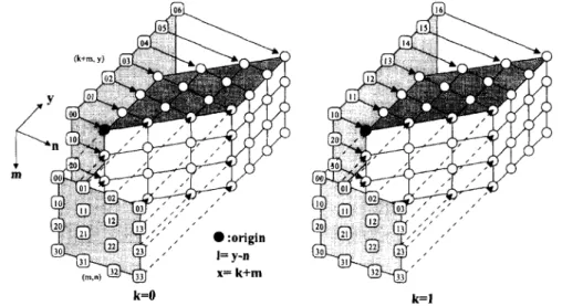
The direct-form DG has four dimensions since template blocks and search areas are both two dimensional. An example DG for
N
=K
=4
is shown in Fig. 2, which is of the same form as the DG in [7] but viewed from a different direction. As the illustration of 4-D graphs is quite complex, several 3- D graphs (sub-DG’s) are sketched instead. The 3-D graphs have the indexes ( m , n , y ) as their axes andk
as the index of each graph. The remaining two indexes, 2 andI ,
can bederived from others.
x
is equal tok
+
m, and l is equal to y - n. As a result, in each 3-D sub-DG, z-axis is parallel with m-axis, and Z-axis is parallel with the plane y+
n = 0. Note that Fig. 2 only illustrates two 3-D sub-DG’s indexed ask
= 0 and 1, while the others, withk
= 2 andk
= 3, are omitted for simplicity. Each sub-DG represents the matching between the template block and four candidate blocks from left to right in the search area (or top to bottom if z is parallel with the vertical axis of frames). Each unit operation, i.e., the combination of a subtraction, an absolute-value, and an accumulation, is denoted by a node. The template block pixels run along the y direction in each sub-DG, and the search area pixels run along the n direction. In other words, the nodes along the y direction receive the same template block pixel, as indicated by the number on the shaded plane over the m-ndomain, while the nodes along the n direction use the same search area pixel, whose index is the number on the shaded plane over the m-y domain. For consecutive sub-DG’s, the working regions on the search area overlap. This can be seen in the sub-DG’s. Each SAD corresponds to the accumulation of all the node outputs over the plane y = n+Z, where 1 ranges from 0 to
( K
- 1). The order of accumulating the node outputs is not specified because it can be changed without affecting the results.The direct-form DG described above is not the unique DG for FSBM. It is a straightforward form and the derived
~
334 IEEE TRANSACTIONS ON CIRCUITS AND SYSTEMS FOR VIDEO TECHNOLOGY, VOL. 5, NO. 4. AUGUST 1995
x= k+m k=O
Fig. 2 . Direct-form dependence graph for full search block matching
architectures can work at high speed and incorporates simple control schemes. However, considering partitionability. serial input and single time access of pixels will simplify input connections. These characteristics will be easier to be achieved if search area pixels are sequentially sketched in one dimen- sion, as it will be more instructive than the direct-form DG, in which the search area pixels appear in three dimensions. The proposed approach to achieve the desired DG is breaking the direct form DG into two-dimensional parts, placing these parts on a plane, and adjusting their relative positions so that the search area pixels are spread in one dimension. Since the same approach is also applied to arrange the template block pixels, the only way to partition sub-DG’s is using m.
index. The resultant 2-D parts (slices) are parallelograms with template block pixels running along one direction and search area pixels running along the perpendicular direction. Each slice is associated with one row of template block pixels and one row of search area pixels, but the association is multiple slices to one row of pixels. The distribution of SAD in different slices will not affect the results because the accumulation can be in any order. This partitioning process is called slicing.
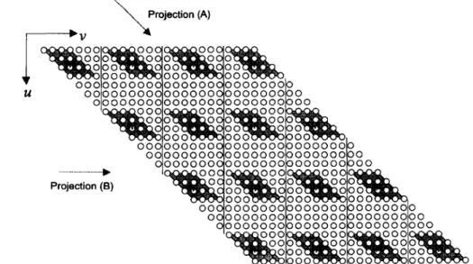
After the slicing process, a new DG is constructed by arranging the relative positions of the 2-D slices on a plane. This process is referred to as tiling. Tiling also replaces one step of projection and scheduling, since two steps are required to derive a 2-D array from the direct-form DG, while only one step is needed after tiling. A typical result of tiling is shown in Fig. 3, where the slices from the same sub-DG are tiled along ( u - u ) = (1, 1). This form was originally illustrated in [15]. The parallelograms enclose the nodes of the slices, which consist of operations, while the nodes outside represent no-operation (NOP) states except for data transferring. The two numbers over each slice are the corresponding k and m.
which indicate the sub-DG that the slice comes from, and the position of the slice in the sub-DG, respectively. In each slice, the nodes along the U direction use the same search
area pixel, and those along the ‘U direction use the same
current block pixel. As the association of slices with pixels is multiple to one, the alignment of slices, in this figure,
k=I
makes each search area pixel runs along the U direction,
and each template block pixel runs along the
v
direction. The vertical lines separate the different rows of search area pixels. The operations of each SAD are distributed along( U . U) = (1, 1) direction. 2-D array architectures can be
achieved with projection along any direction, but only (0,l) and ( I , 1 ) are reasonable, because others obviously result in architectures with very low utilization. The scheduling can also be performed along many directions, but it is not described here because it affects timing only.
In addition to the above example, other DG’s can be found in a similar way. Fig. 4 shows an alternative tiling arrangement, in which the slices of each sub-DG are tiled along the v direction. For example, the slices of the first sub- DG, k = 0, constitute the first row of slices. Thus, the search area pixels still run along the U axis, but the template block
pixels and the operations of a SAD are not aligned as in Fig. 3.
For the slices that are tiled along the U direction, the associated
row of pixels in the template block is different for different slices. On the other hand, the slices along ( U : w) = (1.1) are
associated with the same row of pixels in a template block. As a result, the template block pixels run horizontally inside slices only, but not in the entire DG. For example, c(0,O) is used by the first row of nodes in slices (O,O), (1,0), (2,0), (3,O). The operations of a SAD are not aligned in one line as in Fig. 3. For example, SAD(0,O) is distributed in the left-most diagonal nodes of slices (O,O), (0, I), (0,2), (O,3). Reasonable projection directions are also ( U , w ) = (0, 1) and (1,l). Nevertheless, the
resultant architectures exhibits different characteristics from those of Fig. 3. More variations due to scheduling can be found in [16].
Although the above DG’s are focused on full-pixel FSBM, it is also possible to accommodate them to some algorithms that are based on subsampled template blocks or search areas, if these algorithms still have regular operations. As each node consists of two input pixels, if one of the pixel does not exist, this node can be removed or replaced by an NOP node, and it is possible to use less hardware. The techniques that are used to manipulate DG’s of full-pixel FSBM are still usable.
CHANG ef al.: SCALABLE ARRAY ARCHITECTURE DESIGN FOR FULL SEARCH BLOCK MATCHING 335
Projection (A)
Fig. 3. Transformed DG for type A and B architectures. Note: (U. U ) is to indicate directions and does not have relationship with data or operation.
Projection (C) I v
I
lo U 0 0 0 0 0 0 0 0 0 0 0 0 0 0 0 0 0 0 0 0 0 0 0 0 0 010 0 0 0 0 0 010 0 0 0 0 0 010 0 0 0 0 0 010 0 0 ProjectioiFig. 4. Transformed DG for type C and D architectures. Note: (U, U) is to indicate directions and does not have relationship with data or operation.
However, such algorithms are usually followed by fine-search, which needs much fewer operations, and the sequence of data access is not regular. Consequently, array architectures are not suitable to handle them, and some special hardware is required [201.
B. Class$cation of 2 - 0 Array Architectures for FSBM
In the previous subsection, two reasonable projection di- rections are indicated to accompany each transformed DG.
Each projection direction can produce one type of 2-D array architecture with specific characteristics. Therefore, four types of 2-D array architectures are available by combining two tiling approaches and two projection directions, but the four combinations do not cover all possibilities. As the number of
PE’s in a 2-D array architectures is related to N or K in either dimension, the architectures can be classified according to the assignment of unit operations to PE’s and the execution order
in each PE. To define this classification, FSBM is represented in loops as follows.
Initialization, SAD(IC,
1)
= 0 for all IC, 1. for IC = 0 to K-
1 for1
= 0 toK
- 1 for m = 0 to N - 1 for n = 0 toN
- 1 SAD(lc, 2 ) = SAD(lc,1)
end n+f(k
4
m, n ) end m end 1 endIC
Find
(i,
i)
such that SAD(k,i)
= min{SAD(IC, 1 ) )for all (IC, 1).
where f ( k , Z , m , n ) = Ic(m,n) - p ( k
+
m,l+
n)l, and336 IEEE TRANSACTIONS ON CIRCUITS AND SYSTEMS FOR VlDEO TECHNOLOGY. VOL. 5. NO. 4. AUGUST 1995
four dimensions, the mapping from FSBM to a 2-D array architecture is equivalent to taking two indexes as the indexes of PE’s and setting the order of the remaining two indexes as the loop indexes for the operation sequence in each PE. Thus, C;.:! or twelve different combinations can be found. For simplicity, the relative orientation of the template blockhearch area to the image frames is not defined temporarily. Thus, the twelve combinations are not unique, but fall into six categories. For example, if X . I is taken as the indexes of PE’s, taking
rrt,. ‘ti as the loop order is equivalent to taking 71, rrt, as the
loop order. The influence of the relative orientation to frames is important when we need to consider the relationship of data flows between consecutive template blocks. This part is presented in the appendix. The notation for the assignments of operations to PE’s is of the form f ( k . 1 .
*,
*), which means all the f s with the 4ame k and I are assigned to PE ( k , 1). The operation sequence is denoted by siii + ‘it,. which means frr) is the outer loop, and 7) is the inner loop. The six types ofarchitectures. including their numbers of PE’s, are described as follows. Typical designs are also indicated. Designs of the same types may not be equivalent in every aspect because global timing is not considered in this classification.
Type A: f ( X 1 , 2:. ”) Number of PE’s: Typical designs: Type B: f ( ” ,
”,
T t l , . n ) , Number of PE’s: Typical designs: Type C: f ( * , 1. 111. >k), f ( * , 1 . 7 1 1 . *), Number of PE’s: Type D: Number of PE’s: Typical designs: Type E: , f ( * , 1.*,
i t , ) , Number of PE’s: Typical designs: Type F: f ( * . 1.*.
I t , ) , Number of PE’s: 111 --i I 1 K x K . Type 2 in 191, [171, [IS]. k + l 1v x N . AB2 in [ 7 ] , Type 1 in [9], [IO], [19]. A: + ‘ri K x N . k --i 711 K xAV.
AS2 in [ 7 ] . / I / + h: K x N .Among the six types, Types A to D can be easily repre- sented using the DG’s transformed by S&T, as indicated by Figs. 3 and 4. However. Types A and D cannot be easily expressed with simple projection operation on the direct-form DG, because different sub-DG’s must be considered together. Although Types B and C can also be expressed with the direct-form DG and projection directions along :y axis and the direction of y - ‘11 = 0. respectively, transformed DG’s
are preferred because some manipulation techniques of DG’s are available. Fig. 3 also shows the two projection directions to produce Types A and B architectures, and Fig. 4 shows the two projection directions to produce Types C and D. Types E
U U U U U uuuu 0 0 0 0 0 0 0 0 0 0 c‘ooooooo 0 0 0 0 3 0 0 0 0 0 0 0 0 0 0 ocOoooo3c3oc 000030000c00
Fig. 5 . Another form of DG for Type D architecture to eliminate no-operation states between slices.
and F can be achieved through the projection of the direct form DG along the rrt direction, but with different scheduling. Type E is achieved by scheduling sub-DG’s one-by-one, while Type F is achieved by scheduling them in an interleaved way. S&T is not suitable for the two types because on the direct-form DG, nodes along the vi direction are distributed in different
slices after slicing using the mi index, while slicing using other
indexes does not offer advantages for arranging the data flows of both template blocks and search areas.
C. Selection of the Architecture
The data in FSBM consist of template block pixels, search area pixels, and partial sums of SAD’s. Considering 2-D arrays, the transfer of data may be different along differ- ent directions. Since our target is a cascadable architecture, the array must be partitioned, and the connections between partitions should be simplified. Consequently, the results of partitioning are used to judge architectures. It is assumed that arrays are two-dimensional and rectangular. Considering search area pixels, Type E and Type F are not suitable for partitioning because the data are shared by the PE’s along 45” direction, e.g., AS2 in [ 7 ) , and therefore, either horizontal or vertical partitioning produces many connection lines across the boundary. For Types A, B, C, and D, since the search area pixels may be shared by all PE’s, fewer connections are required after partitioning. This result can be seen in the proposed architecture. The second to be considered is the distribution of the unit operations of SAD’s. Separating the unit operations of one SAD in different partitions requires extra connection lines in-between. For this reason, Types B and C are not suitable because partitioning separates the unit operations of one SAD in different parts. This can be seen for Type B, if the DG in Fig. 3 is divided into upper and lower parts, and for Type C, if the DG in Fig. 4 is divided along the diagonal direction.
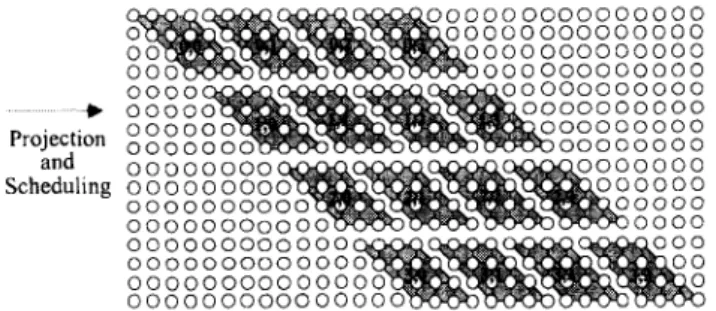
Figs. 3 and 4 consider serial input of search area pixels only. However, the resultant PE utilization is quite low because many NOP nodes are projected onto PE’s. To achieve 100% utilization, the only way is to have the slices abut. An example for Type D is shown in Fig. 5 , where the NOP nodes are overlapped with slices. As the SOP nodes and the OP nodes both imply data transferring, the result is that two search area pixels are simultaneously carried by the PE’s. For the PE’s that come from the first row of slices, (0,O) to (0,3), two data
CHANG et al.: SCALABLE ARRAY ARCHITECTLTRE DESIGN FOR FULL SEARCH BLOCK MATCHING 331
Projection ’
a I
Fig. 6 . DG for Type A and 8 x 4 array after partitioning slices. The scheduling direction makes search area pixels broadcast in each 1-D array.
+”
I
*
Projection and Scheduling
Fig. 7. DG for Type D and 8 x 4 array after partitioning slices. The scheduling direction makes search area pixels broadcast in each 1-D array.
lines will be required. These lines are called main lines, and the 1-D array of PE’s that comes from one row of slices is called a module. The other modules can share the data with the previous modules, but for slice (1,3), (2,3), (3,3), the data do not exist in the upper slices. Consequently, each of the modules that execute these slices needs an extra connection to the input source. As these modules do not use the extra connection lines simultaneously, these lines can be connected with fewer lines that are actually linked with the input source. The latter lines are called force lines because the data can ovemde those coming from the previous module. In Fig. 5, the array will require two main lines and two force lines, since two of slices (1,3), (2,3), (3,3) are executed simultaneously at most.
For a modular design with variable sizes of search area, each slice of Type A must be further divided into N x N parallelograms. Otherwise, each module will consist of K PE’s, and the number of main lines increases as
K
grows to some extent. For example, three main lines is needed ifK
= 2N. When Type D is compared with Type A, Type D requires a local buffer of size K for each module to store temporary results of SAD’S, but Type A does not need such buffers. However, when K is larger than N, and the array size is larger than N x N, Type A requires more force lines than Type D if implemented in the target connection style. Figs. 6and 7 explain the results for Type A and Type D when K is 8,
N
is 4, and the array sizes are both 8x 4. In Fig. 6, each slice has been partitioned into two 4 x 4 parallelograms. The first row of slices denotes the task of the previous template block, and the second row to fifth row represent half part of a complete DG. The other half part starts from the sixth row, so that a complete job is accomplished in two steps. As Type A uses the projection direction ( l , l ) , the 1-D array that comes from one diagonal string of slices is a module, which consists of N PE’s. Note that since scheduling is along ( U ,w)
= (0, l ) ,each slice is shifted one node right away from its left neighbor so that the search area pixels will not be broadcast to every PE. Each module will receive search area pixels with one cycle delay after the previous module. In this figure, the slices (1,3), (2,3), (3,3), (4,3), (5,3), (6,3), and (7,3) must use force lines because no other slices access the same data before them. As the same reason also holds for the previous job, i.e., the white slices, it can be seen that totally four force lines are required. Fig. 7 shows the DG for Type D, but no partitioning is employed because this DG makes a K x N array. The white slices also denote the previous task. To avoid broadcasting data to the entire array, each row of slices is moved one node right from its upper neighbor. The slices that use force lines are still (1,3), (2,3), (3,3), (4,3), (5,3), (6,3), and (7,3). From this figure, it can be seen that three force lines are enough. As a
-
338 IEEE TRANSACTIONS ON CIRCUITS AND SYSTEMS FOR VIDEO TECHNOLOGY. VOL. 5. NO. 4, AUGUST 1995
I I 1st position. SAD. MV 1st position, SAD. M V
L
1
D f l1
- Pf2 WI st osition index of the first candidare black that IS asslgned to thls module SAL. MV local minimal SAD and the corresponding motion vecfor
Fig. 8. Two chips cascaded
result, Type D is adopted in the architecture design to reduce the maximal number of force lines.
In Figs. 6 and 7, scheduling directions are both (0,l) to make search area pixels broadcast inside each module, other directions can be adopted to avoid broadcasting. For example, (-2,l) will result in delay elements between PE’s for both template block and search area pixels. On the other hand, the tight abutment of the DG’s of the current task and the previous task, i.e., the white slices, indicates that the processors are not idle when one task ends.
If search areas are centered at the positions of corresponding template blocks on the picture, there will be overlap between adjacent search areas. This overlap can be exploited to reduce input bandwidth. The explanation is in the Appendix.
111. THE PROPOSED ARCHITECTURE
The proposed architecture is constructed by cascading mod- ules of PE’s with simple connections, and several numbers of cascaded modules are allowed, depending on the demanded computing power. Moreover, some frequently used tracking ranges are supported. Therefore, the design would be more economical and efficient than specific architectures for desig- nated applications.
This section is divided into two subsections. Section III- A describes the architecture and data flow. The connection of modules and the structures of PE’s are presented, and the flows of different data are explained, including the operation modes for different tracking ranges and numbers of modules. Section 111-B presents a typical input buffer design that can act as a bridge between the data source and the processors.
A . Connection and Datu Flow
The connection style for transfemng input data is serial cascading, which requires fewer data lines from the input buffer and enables modules to be attached or removed with minor global change. Fig. 8 shows the connection of two chips and the host. The global data lines are force lines to sustain optimal utilization. The input data, either template blocks or search areas, are sent to the first module, which transfers the data to the second module, and then further ones. The local
minimal SAD and the corresponding motion vector of each module are compared with those from the previous module, and the results are transferred to the next module. The output of the last module is directed to the host, which controls the overall timing and input data sequences. If fewer modules are used, each module must be responsible for several rows of SAD’S. In this case, the host will feed the partial results received from the last module into the first module to update the data for more rounds.
Fig. 9 shows two modules cascaded inside a chip. pl and p 2 are main lines, which are from the previous chip, and p f l and p f 2 are force lines. Each module has two buses for search
area pixels. The upper module has busl directly connected to p l . and bus2 connected to either p 2 . p f l , or p f a . On the other hand, the lower module has bus3 connected to bus2 and has
bus4 connected to either busl, p f l , or p f 2 . bus3 and bus4
are also connected with p l and p 2 of the next chip. For an array of fewer than N modules, every two modules can be connected in the same way.
An example DG of the proposed architecture is shown in Fig. 10 for N =
K
= 4 and a 4 x 4 array, i.e., four modules with four PE’s in each module. As explained in Fig. 7, all NOP nodes are covered with OP nodes to ensure 100% utilization, and each row of slices is further shifted one node right from the upper row to prevent broadcasting each search area pixel to all PE’s. The first module comes from the slices (O,O), (0,1), (0,2), (0,3), in which main lines are used, while the other modules use force lines when executing the slices (l,3), (2,3), (3,3).In this example, two force lines are sufficient, because when scheduling through the DG, only two slices, e.g., (1,3) and (2,3), need to use force lines simultaneously.
The input sequence on the main lines and force lines is illustrated in Fig. 11 for an array of four modules. The light- gray squares denote the data for the current motion vector, dark-gray squares are for previous or next ones, and white squares mean no data on the buses. Each string of light-gray squares is assigned a number to indicate its row index in the search area. The sequence is row-wise but overlapped. When a PE receives the selection signal, it switches to the other bus to access a new row of search area pixels.
The data Row of template block pixels is different from that of search area pixels. In each module, a PE uses a specific
339
CHANG et al.: SCALABLE ARRAY ARCHITECTURE DESIGN FOR FULL SEARCH BLOCK MATCHING
First
M v SAD,
r - - - -
: m
_ _ _ _ _ _ _ _ _ _ _ _ _ _ _ _ _ _ _ _ _ - - - _ - - - : parallel in serial out
I
I
v
threestatebuffer II semal in parallel out
I
’ delay element II
Fig. 9. Two modules cascaded inside chip.
Fig. 10.
exists. The white slices are for the next template block.
DG of the proposed architecture with N = K = 4. No NOP nodes
f P2 C C P l P2 Pfl (global) Pf2 (global)
~ delay element Ej Dfltp-flop ’ I V time-statebuffer Tfllpflop I
P I ...-... .... ...-... - - - -
PZ Fig. 12. Internal structures of PE’s.
Pfl
Pfi
: prevlous or next
area.
column of pixels, and each pixel is used for
K
cycles. Since the same sequence is used in all modules, the data can be shared between modules, and individual lines to the input buffer are not needed. The template block pixels are sent to the PE’s through a bus in the first module of a chip, because only one PE needs to latch a template block pixel at a time. The other modules on the same chip receive the data through PE-to-PE connections, and the last module transfers the pixels to thenext chip through a bus. The selection signal for search area data is also used here to control the latch. No other control signal is needed.
For SAD’s, one module is responsible for one row of
SAD’s, and each PE executes a specific column of operations in every SAD assigned to the module. Only the local minimal
SAD and the corresponding motion vector need to be trans- ferred between modules. In each time slot, each PE calculates one pixel difference and its absolute value and adds this result
340 IEEE TRANSACTIONS ON ClRCUITS AND SYSTEMS FOR VIDEO TECHNOLOGY, VOL. 5, NO. 4, AUGUST 1995
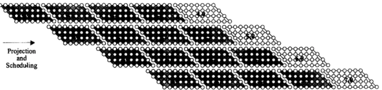
Fig. 14. DG for larger search area and our modules with Ai = 4. li = 8. The white nodes are the second round for the same motion vector
to the partial sum received from the right neighboring PE of the same module. The new partial sum is sent to the PE on the left side at the next time slot. Since there are N PE’s in a module, the final result at the left-most PE is the accumulation of only one row of pixel differences associated with one SAD. Then, the module proceeds with the same row of pixel differences associated with another SAD. Because the SAD’s are not completed for comparison, each module includes a buffer of size K to store the partial sums and an accumulator to update the sums. The buffer size must be variable if the modules are to be used for different tracking ranges.
Other information transmitted to the next module includes an index that indicates the row of SAD’s assigned to the next module. This index is incremented and sent to the further modules. In addition, the minimal value of the SAD’s and the corresponding motion vector are also sent in the same way.
The internal structure of the PE’s is sketched in Fig. 12. The left PE is for the upper module, and the right PE is for the lower module. If more modules are implemented in a chip, a third type of PE needs to be designed. Except for the template block path, the data paths are equivalent in the two kinds of PE’s. The selection signal is received from the right PE and sent to the left one.
For different demands of computing power and tracking ranges, the modes of this architecture can also be explained using DG’s. The cases when K
>
N and K x N PE’s have been explained in Fig. 7, in which K = 8, N = 4, and the array size is 8 x 4. Although the minimal number of force lines is three, it is more regular to divide the array into groups ofN
modules each, so that each group uses two force lines. If half computing power is enough, the DG in Fig. 10 can be modified to Fig. 13, where the slices, (2,”) and (3,*), are moved to the left of (O,*) and (l,*) so that two modules are used. For K = 8, N = 4 and four modules, the DG is shown in Fig. 14. In these examples, it can be seen that all the partitions of DG are of the same shape and size. This rule is to keep data flow consistent in every partitioned task. Although irregular partitions provide much higher flexibility, it also complicates the design. Following this rule limits the possible numbers of cascadable modules, e.g., 1, 2, 4, and 8 forK
= 8,N
= 4. On the other hand, PE count in a module is also limited to N for Type D.B. Organization of Input Buffers
The input buffer acts as a bridge between the signal source, e.g., the frame buffer, and the processors so that only simple data sequences need to be provided from the signal source. The
input data consists of template block and search area pixels. The template block has fewer pixels, so two memory banks working alternately in read and write modes are sufficient. However, the input buffer for the search area is more complex because it has several times more pixels. Furthermore, in the proposed architecture, four external data lines are connected to the input buffer when
N
modules are used. A typical memory organization is proposed to the convert simple input sequences to the desired ones. This organization can also provide different data sequences for various sizes of search areas and various numbers of modules from one toN .
Further modifications can be made if more modules are cascaded. The advantage of search area overlap is not utilized because of flexibility reason. For example, in MPEG, the time distance for motion estimation may be more than one frame, but the tracking range cannot increase in proportion to the time distance. Otherwise, the computational load will also increase in proportion. As a result, the location of the search area on the frame might have to be determined through prediction, instead of regularly positioned [21].For nonoverlapped search areas, the average input rate of search area pixels can be found by dividing the total number of pixels by the block pipeline period. Assume
K
is larger than or equal to N , as in most cases. The block pipeline period of the proposed architecture is r K / $ ] N K , where N is the number of modules; if K is a multiple ofN ,
the shortest block pipeline period isK 2 .
Since the number of pixels is ( N+
K - 1)2, the input rate can be proved to be lower than four pixels per time slot, which matches the usage of four data lines. The organization of this buffer is shown in Fig. 15. Two pairs of output lines, p l , p 2 and p f l , pf2, are provided by the two groups of memory blocks, called upper clusters and lower clusters. The upper clusters have two duplicates and the lower clusters have three so that all the pixels of a search area are available when the computation of a motion vector starts. The upper clusters store only the data for the current and next motion vectors, while the lower clusters have to store the data for the previous, current and next motion vectors. This arrangement is to support the pipeline of the architecture. Each upper cluster can store N ( N+
K,,,) pixels, and each lower cluster can storeK,,,(N
+
Kmax),
whereK,,,
is the maximal value ofK
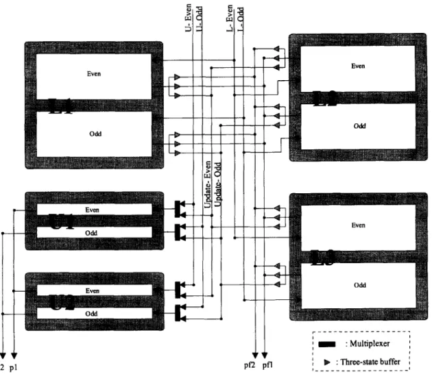
allowed. Thus, one upper cluster and one lower cluster can hold an entire search area. Moreover, a cluster is divided into an even bank and an odd bank for the even and odd rows of pixels, respectively. Each bank allows reading and writing simultaneously, so a cluster can provide two pixels at a time.CHANG et al.: SCALABLE ARRAY ARCHITECTURE DESIGN FOR FULL SEARCH BLOCK MATCHING
~
34 1
f
wP2 Pl
Fig. 15. Input buffer for search area.
Fig. 16. Data squence of input buffer for search area.
The upper clusters can accept data either from the signal source or from the lower clusters, because some of the data in the lower clusters may be sent through pl or p 2 . This internal transfer is accomplished through the two buses,
Update-Even
andUpdate-Odd.
Fig. 16 depicts the timing of the output portsand intemal buses in the input buffer with N = 4,
K
= 8, and four modules. p f l and p f 2 are not used very often, because in this case, some of their data are the same as those on pl and p2.As this memory organization is expected to satisfy several processing modes, it is designed to provide different data
sequences. Further pruning is needed if the architecture is used for dedicated modes.
IV. CHIP DESIGN
In the realization of this architecture, a module consists of sixteen PE’s because a 16
x
16 block is often adopted, and the tracking range can be 16x 16, 32x 32, or 6 4x 64. Two modules are implemented in a chip.The major building blocks of the architecture are the PE’s,
~
342 IEEE TRANSACTIONS ON CIRCUITS AND SYSTEMS FOR VIDEO TECHNOLOGY, VOL. 5 , NO. 4, AUGUST 1995
Fig. 17. Layout of the chip with two nodules.
TABLE I CHIP CHARACTERISTICS Block size 16 x 16 Tracking range Die size Transistor count 102 K Pin count 100 16 x 1 6 , 3 2 x 32,64 x 64 6.44 x 5.26 mm2
(PISO) circuits. The SIP0 and PIS0 circuits are to transfer in bit(s)-serial between chips the local results and the indexes of the starting SAD that is assigned to the modules, since these are a small amount of data. The buffers for temporary results are variable length delay lines that can store 16, 32, or 64 16-b words, depending on the tracking range. Two types of PE’s are designed as described in Section 111. The subtractor for pixel differences is 8 b long, and the accumulator is a 16- b adder. Since the partial results from the previous PE must wait for the output of the subtractor, the most significant eight bits of the accumulator in the previous PE are delayed one time slot and finished at the same time as the subtraction of the current PE. Consequently, the delay in the accumulator is changed from a 16-b addition to an 8-b one, and the path that contributes most delay in the PE consists of two 8-b adders plus two multiplexers.
The chip layout is illustrated in Fig. 17. The die size is 6.44 x 5.26 mm2 with 101 540 transistors in 0.8 pm technology, and the pin-count is 100. These characteristics are also listed in Table I.
V. CONCLUSION
Full search block matching is a widely used motion estima- tion algorithm in current video systems because of its better performance and high regularity. This paper presents a pro- cedure for designing architectures for FSBM. More solutions can be found, and the arrangement of timing can be simplified with the aid of dependence graphs. The proposed procedure is also used to design of a scalable architecture. Since different applications demand different levels of computing power, this architecture is constructed by cascading modules of processing
elements, so that the number of processing elements can be varied. In addition, several tracking ranges are supported, and the utilization of processing elements is optimized. These characteristics make the resulting architecture efficient and economical, as the hardware can be applied in a wide range of applications.
Although this architecture offers high flexibility, it is not intended to be a universal or optimal one, but rather a step- ping stone for further modification by applying the proposed design procedure. The architecture described here can serve as a foundation for developing more satisfactory designs for different applications.
APPENDIX
In some cases, the position of a template block on an image frame is at the center of search area. This results in overlap of search areas for consecutive template blocks, and the overlap is usually exploited to reduce the size of input buffer or input bandwidth [ l l ] , [13], [18]. For two horizontally abutted template blocks, their search areas have an overlap of ( K - 1) columns of pixels. As a result, to utilize this characteristic, it is better to access search area pixels column-by-column so that the addressing of input buffer can be simplified. If the architecture is a nonpartitioned array, overlap can also be used to reduce number of data lines. For example, in Fig. 5, assume that each slice is associated with one column of pixels. Slices (O,O), (O,l), (0,2), (0,3), (1,3), (2,3), and (3,3) are associated with column 0, 1, 2, 3, 4, 5, 6, respectively. For the next template block, its DG will have slices (O,O), (O,l), (0,2), (0,3), (1,3), (2,3), and (3,3) associated with column 4, 5, 6, 7 ,
8,
9, 10, respectively. If the second DG abuts the first DG on the left side, it can be seen that slices (1,3), (2,3), (3,3) of the first DG have exactly the same associations as slices (O,O), (O,l), (0,2) of the second DG. Consequently, the force lines are not needed, and only two pixels need to be accessed at a time.For template blocks, because of fewer pixels and no overlap, not much advantage can be gained. Although camera output is line-by-line, since each block occupies
N
lines, a buffer is still required between the camera and processors. Therefore, the access pattern, e.g., row-by-row or column-by-column, is not important.REFERENCES
H. Gharavi and M. Mills, “Blockmatching motion estimation algo- rithms-New results,” IEEE Trans. Circuits Syst., vol. 37, no. 5 , pp.
649-651, May 1990.
M.-J. Chen. Y.-P. Lee, L.-G. Chen, and T.-D. Chiueh, “VLSI implemen- tation of real-time motion estimation for video compression,” in Proc.
Fourth VLSI DesigdCAD Workshop, Taiwan, Aug. 1993, pp. 129-133. A. N. Netravali and B. G. Haskell, Digital Pictures: Represenration and
Compression. New York: Plenum, 1988.
M. Ghanbari, “The cross-search algorithm for motion estimation,” IEEE
Trans. Commun., vol. 38, no. 7, pp. 950-953, July 1990.
L. G. Chen, W. T. Chen, Y. S. Jehng, and C. T. Chuch, “An efficient parallel motion estimation algorithm for digital image processing,” IEEE
Trans. Circuits Syst. Video Technol., vol. 1, no. 4, pp. 378-385, Dec. 1991,
L. W. Lee, J. F. Wang, J, Y. Lee, and J. D. Shie, “Dynamic search- window adjustment and interlaced search for block-matching algo- rithm,” IEEE Trans. Circuits Syst. Video Technol., vol. 3, no. 1, pp. 85-87. Feb. 1993.
CHANG et al.: SCALABLE ARRAY ARCHITECTURE DESIGN FOR FULL SEARCH BLOCK MATCHING 343
[7] T. Komarek and P. Pirsch, “Array architectures for block matching algorithm,” IEEE Trans. Circuits Syst., vol. 36, no. 10, pp. 1301-1308, Oct. 1989.
[8] C. H. Chou and Y. C. Chen, “A VLSI architecture for real-time and flexible image template matching,” IEEE Trans. Circuits Syst., vol. 36, no. 10, pp. 1336-1342, Oct. 1989.
[9] L. De Vos and M. Stegherr, “Parameterizable VLSI architectures for the full-search block-matching algorithm,” IEEE Trans. Circuits Syst., vol. 36, no. 10, pp. 1309-1316, Oct. 1989.
[IO] C. H. Hsieh and T. P. Lin, “VLSI architecture for block-matching motion estimation algorithm,” IEEE Trans. Circuits Syst. video Technol., vol. 2, no. 2, pp. 169-175, June 1992.
[ l 11 S. Uramoto, A. Takabatake, M. Suzuki, H. Sakurai and M. Yoshimoto, “A half-pel precision motion estimation processor for NTSC-resolution video,” Proc. IEEE 1993 Custom Integrated Circuits Cont. 1993, pp.
11.2.1-1 1.2.4.
1121 A. Artieri and 0. Colavin, “A chip set core for image compression,”
IEEE Trans. ConsumerElectron., vol. 36, no. 3, pp. 395402, Aug. 1990. [13] C. M. Chen, Y. C. Chen, and H. H. Shen, “VLSI architecture design of a high-speed motion estimator for HDTV application,” in P roc. 1993 Inc. Symp. Commun., Hsinchu, Taiwan, vol. 2, pp. 19-9-19-16, 1993. [ 141 S. Y. Kung, VLSZ Array Processors. Englewood Cliffs, NJ: Prentice-
Hall, 1988.
[15] G. Privat and M. Renaudin, “Motion estimation VLSI architecture for image coding,” in Proc. Int. Con5 Comput. Design: VLSI Comput. Processors, 1989, pp. 78-81.
1161 S. Chang and C. W. Jen, “On the VLSI array architectures for full search block matching,” in Proc. IEEE Asia-Pacijc Con5 Circuits Syst., 1992, pp. 319-323.
[17] H. Fujiwara, M. L. Liou, M. T. Sun, K. M. Yang, M. Maruyama, K. Shomura, and K. Ohyama, “An all-ASIC implementation of a low bit- rate video codec,” IEEE Trans. Circuits Syst. video Technol., vol. 2, no. 2, pp. 123-134, June 1992.
[18] P. A. Ruetz, P. Tong, D. Bailey, D. A. Luthi, and P. H. Ang, “A high-performance full-motion video compression chip set,” IEEE Trans.
Circuits Syst. video Technol., vol. 2, no. 2, pp. 11 1-122, June 1992. [19] L. De Vos and M. Stegherr, “Systolic block-matching architectures
for large maximum displacements,” in Algorithms and Parallel VLSI
Architectures, Proceedings, vol. B. Amsterdam: Elsevier, 1991, pp. 221-228.
1201 K. M. Yang, M. T. Sun and L. Wu, “Family of VLSI designs for the motion compensation block-matching algorithm,” IEEE Trans. Circuirs
Syst., vol. 36, no. 10, pp. 1317-1325, Oct. 1989.
1211 Y. Q. Zhang and S. Zafar, “Predictive block-matching motion esti- mation for TV coding-Part 11: Inter-frame prediction,” IEEE Trans.
Broadcasting, vol. 37, no. 3, pp. 102-105, Sept. 1991.
Shifan Chang received the B.S. degree in electron-
ics engineering from National Chiao Tung Univer- sity, Hsinchu, Taiwan, in 1989.
He is currently working on the Ph.D. degree in electronics at National Chiao Tung University. His research interests include image processing, video applications, parallel processing, and VLSI architecture design.
Juin-Haur Hwang received the B.S. degree in
electrical engineenng from National Cheng Kung University, Tainan, Taiwan, in 1991, and the M.S.
degree in electronics engineering from National Chiao Tung University, Hsinchu, Taiwan, in 1993. He is with VIA Technologies, Inc., Taiwan. His research interests include computer architecture and VLSI design.
Chein-Wei Jen (S’78-M’84) received the B.S. de-
gree from National Chiao Tung University in 1970, the M.S. degree from Stanford University, Stanford, CA, in 1977, and the Ph.D. degree from National Chiao Tung University in 1983.
He is currently with the Department of Elec- tronics Engineering and the Institute of Electronics, Nahonal Chiao Tung University, Hsinchu, Taiwan,
as a Professor. During 1985-1986, he was with the
ty of Southem California, Los Angeles, as g Researcher. His current research interests include VLSI design, digital signal processing, processor architecture, and design automation.