國
立
交
通
大
學
電機學院光電顯示科技產業研發碩士班
碩
士
論
文
五環素沈積溫度對有機薄膜電晶體電性影響之研究
Effect of Deposition Temperature on the Device Properties of
Pentacene Thin-Film Transistors
研 究 生:陳映頻
指導教授:陳方中 教授
五環素沈積溫度對有機薄膜電晶體電性影響之研究
Effect of Deposition Temperature on the Device
Properties of Pentacene Thin-Film Transistors
研 究 生:陳映頻 Student:Ying-Pin Chen
指導教授:陳方中博士 Advisor:Dr. Fang-Chung Chen
國 立 交 通 大 學
電機學院光電顯示科技產業研發碩士班
碩 士 論 文
A Thesis
Submitted to College of Electrical and Computer Engineering National Chiao Tung University
in partial Fulfillment of the Requirements for the Degree of
Master in
Industrial Technology R & D Master Program on Photonics and Display Technologies
May 2007
Hsinchu, Taiwan, Republic of China
五環素沈積溫度對有機薄膜電晶體電性影響之研究
學生: 陳映頻 指導教授: 陳方中
國立交通大學電機學院產業研發碩士班
摘
要
本研究以沈積溫度為變因,探討五環素未經歷嚴重晶相變化時,晶粒形貌對 薄膜電晶體電性的影響。除了部分嚴重相變與高於表面處理物玻璃轉移溫度的元 件外,電洞遷移率與橫向晶粒都有隨溫度升高而增加的趨勢。透過電阻萃取的方 式,我們得到下述結果:通道電阻隨溫度升高而下降,此為升溫增大橫向晶粒所 致;接面電阻亦隨晶粒增大而降低;塊體電阻則與晶相變態的嚴重程度有關。此 外,基板經表面處理的電晶體,即使表面晶粒相似也可大幅提昇遷移率。 對表面處理的基板而言,平躺五環素的發生是一重大特徵。過去的研究仍未 明確指出此位向的分子對傳輸機制有何影響。另外,文獻表示五環素於二氧化矽 基板之縱向成長為丘狀成長,此將造成較深的縫道(晶界),而丘狀形貌也是 Ehrlich-Schwoebel 能障存在的表徵。 我們使用AFM 觀察 8nm 厚(五層分子)的五環素試片,發現經表面處理的試 片,其五環素晶界間有模糊化的現象,這暗示了當平躺分子存在時,E-S 能障降 低。我們認為平躺五環素的存在能提昇遷移率的原因,在於此時五環素塊體的晶 緣(step edge),其 E-S 能障較低,使得晶界填補較為容易。因此,即使平躺位 向之分子可能導致基板表面的排列較亂,但遷移率仍舊可提升,這說明了晶界對 遷移率而言仍為最具支配力的因素。
Effect of Deposition Temperature on the Device Properties
of Pentacene Thin-Film Transistors
Student: Ying-Pin Chen Advisor: Dr. Fang-Chung Chen
Industrial Technology R & D Master Program of
Electrical and Computer Engineering College
National Chiao Tung University
ABSTRACT
By varying the temperature during the deposition of pentacene, the effect of substrate temperature on the electrical performance of OTFTs, without serious disturbance of phase transition of pentacene is investigated.
First, the channel resistance is sensitive to the deposition temperature due to the difference size of grains. Second, the contact resistance reduces with increasing deposition temperature, which is likely attributed from the difference of the molecular orientation. Finally, the bulk resistance is more fluctuant to the deposition temperature for P MS -treated devices, whereas the case for HMDS-treated ones is less fluctuant probably arising from phase boundary.
Additionally, the existence of flat-lying pentacene is an important characteristic for the treated devices. However, it is unclear what role the in-plane π system plays. Based on Ehrlich-Schwoebel barrier effect, mound growth governs the vertical evolution, forming deeper crevices. According to the AFM images of initial layer, it suggests that flat-lying pentacene could lower the E-S barrier, leading to shallow boundaries. Consequently, effect of grain boundary is still the most dominant factor to the mobility.
Acknowledgement
研究所入學通知好像上星期才剛收到,兩年五千次的鐘聲卻已經從耳邊飛走 了。這一路的酸甜苦辣,回味無窮卻難以細數。本文順利完成,歸功大家的鼎力 相助,在這邊先向各位說一聲:謝了! 首先衷心感謝我的指導教授-陳方中老師,在科學之路上給予我很大的自 由,並總是適時的拉我一把。最重要的是,兩年過去讓我對自己有青出於藍的期 待。同時謝謝孟心飛老師、戴亞翔老師以及朱治偉博士所提供的寶貴意見,使得 本文更加完備。 接著,我要感謝實驗室學長:謝謝祖榮學長、喬舜學長、文生在知識觀念上 傾囊相授,也謝謝永昇、立仁、東賢在儀器實作上悉心教導,讓我在最短時間內 能夠登堂入室。工欲善其事,必先利其器,我更要特別感謝紓婷、呈祥以及昱仁 協助我對付難纏的AFM,婉琪提供我絕世武器-同幅 XRD,枝福、健富、宗銘 在Matlab 上的指教,才能讓本文畫上完美的句點。 謝謝實驗室的夥伴們:文奎學長、志平學長、尹婷、泰元、浩偉、上傑、瑞 祥、義凱、志力、太獅、曉芬,有你們在,生硬的實驗室增添許多歡樂;也謝謝 這兩年一同作戰的同學們:俞文、佳峰、子怡、卓志、虹娟、明倫……,有你們 在,枯躁的光電子學才走得過去;撰寫論文期間,我要特別謝謝文馨運送糧草支 援,就像驢子推磨一樣,沒有你的蘿蔔我大概推不完了。 謝謝我的電腦小黑,關鍵時刻從不耍脾氣,真是我的最佳戰友。 求學的路走來跌跌撞撞,特別特別感謝爸媽不斷給我安慰打氣,讓我可以支 撐到今天,也謝謝我的兩位二十年老友:昆融、亦桓,時常來電關心,我知道我 不是踽踽獨行。要感謝的人太多了,還是謝天吧! 最後,我要以本文紀念我的好友子怡,雖然我們暫時不能一起吃喝了,但也 許有一天會重逢,我們不會忘記相會時互放的光亮,也祝福你在另一個世界能夠 永遠健康平安,永遠都是最可愛的小白兔。Table of Contents
Abstract (Chinese)……….i Abstract (English)………...………..ii Acknowledgment……….……iii Table of Contents……….…iv Figure Captions……….………….………viii List of Tables……….………xiiiChapter 1 Introduction
1.1 Preface……….…..11.2 Objective and Motivation…..………..…3
1.3 Organization……….……….………4
Chapter 2 Review and Principles
2.1 Organic Thin-Film Transistors………...….52.1-1 Fundamental of Device Physics………..………..……….5
Modeling of the Field-Effect Transistors Limitation 2.1-2 Density of State (DOS)………..………..………6
2.1-3 Static Characteristics and Trapping States………7
Above-threshold & Forward Sub-threshold Region Poole-Frenkle Emission 2.2 Organic Conductors………...………9 2.2-1 Conduction Mechanism…….……..…………..………9 Band Transport Hopping Anisotropy
2.2-2 Crystal Structure………..………..………11
2.3 Pentacene………13
2.4 The Growth of Thin Film………15
2.4-1 The Mechanism of Deposition of Thin-Film…..………15
Nucleation Grain Growth and Coalescence 2.4-2 Fractal-Mound Growth of Pentacene Film..……..………17
Diffusion-Limited Aggregation Ehrlich-Schwoebel Barrier 2.5 X-Ray Diffraction Analysis………19
2.5-1 The Sherrer Equation……….………19
2.5-2 Distortion of the First and Second Kinds…..……..………19
Distortion of First Kind (gI) Distortion of Second Kind (gII) 2.5-3 Paracrystal Theory………20
Chapter 3 Experimental Methods
3.1 Device Fabrication..………..……….………..213.1-1 Preparation of Substrates.……….………21
3.1-2 Surface treatment……….………..………22
3.1-3 Growth of Thin Film and Electrodes…………....…..………..23
3.2 Device Measurement………..……….25
3.3 Instrument and Chemicals………..………25
Chapter 4 Results and Discussions
4.1 Review of Prior Arts……….…………264.2-1 The relationship beween the Deposition Temperature to the grain
Size……….………27
4.2-2 The Mobility Calculation….………..………28
4.2-3 The Transfer Characteristics………….………....…..………..29
4.2-4 The Phase Transition……….30
4.2-5 Conclusion………31
4.3 The Relationship of the Mobility to the Grains……….………33
4.3-1 The Transfer Characteristics without VT Shift………33
4.3-2 Inhibition of Phase Transition………..…..………35
Coherence of Phases Molecular Orientation Intensity 4.3-3 Morphology Evolution……….37
Evolution of Phases Evolution of Grain Shape Evolution of Initial Layers 4.3-4 The Comparison of Mobility………..43
4.4 Channel and Contact Resistance………….……..……….46
4.4-1 Transfer Line Method………46
4.4-2 The Resistance Extraction from HMDS-Treated Device……….47
Channel Resistance Parasitic Resistance Minimum Effective Contact Resistance Bulk Resistance 4.4-3 The Resistance Extraction from P S-Treated Device……….50
Channel Resistance
Minimum Effective Contact Resistance Bulk Resistance
4.4-4 Paracrystal Theory to Study the Bulk Resistance……….53
Paracrystal Theory Lattice Distortion Crystallite Size 4.5 Turn-On Voltage………57
4.5-1 Turn-on Voltage Shift with Surface Treatment………57
4.5-2 Sub-threshold Behavior………58
4.5-3 Turn-on Voltage Shift with Deposition Temperature……….60
Two Gradations of Slope Turn-on Voltage Shift 4.6 Leakage Current………62
4.6-1 Channel Length Dependence of Leakage Current………62
Poole-Frenkel Emission Channel Length Dependence 4.6-2 Gate Voltage Swept in Both Direction……….64
Chapter 5 Conclusion……….66
Appendix.………...…68
Figure Captions
Chapter 1 Introduction
Fig. 1.1. The applications of plastic transistors……...……...1 Fig. 1.2. Evolution of hole mobility for the most common p-type organic
semiconductors.………...……….…………...2
Chapter 2 Review and Principles
Fig. 2.1 Schematic diagram for the TOF system which could measure the carrier mobility directly………...……….…...5 Fig. 2.2 (a) Dependence of field-effect mobility on gate field, E. (b) Dependence of field-effect mobility on charge per unit area, Qs……...…....…………...…6 Fig. 2.3 Density states in the band gap of intrinsic a-Si:H..…………....…...7 Fig. 2.4 The plot of drain current as a function of gate voltage shows four regimes of operation………...………...……...………...…8 Fig. 2.5 Molecular structures of common p-type organic semiconductors…..………9 Fig. 2.6 Carrier transport in the organic semiconductors……...………10 Fig. 2.7 Hole mobility within the a-b plane of pentacene single crystals at room
temperature………...……….…11 Fig. 2.8 Four basic structural types were defined for these planar hydrocarbons.….12 Fig. 2.9 Lewis structure of pentacene……….…13 Fig. 2.10 X-ray patterns, schematic structural order, field effect mobility
corresponding to 3 substrate temperatures……….…13 Fig. 2.11 Common impurity in pentacene. Left: 6,13-dihydropentacene. Right:
Fig. 2.12 The 5 steps of deposition of thin film…………..………....15 Fig. 2.13 The relationship of free energy to radius of grains……….……….16 Fig. 2.14 Wetting angle in the heterogeneous nucleation…………..…….………….16 Fig. 2.15 Coverage-dependent fractal dimension of single-molecular-layer pentacene islands on cyclohexane-saturated Si(001)…………..……….18 Fig. 2.16 The cross section of a monatomic step in a surface and the hypothetical potential associated with the diffusion of an atom over such a surface…...18 Fig. 2.17 (Left) A simulated surface without the presence of the Ehrlich- Schwoebel barrier, (Meddle)A simulated surface approaching real situation, (Right) Fourier transform of a typical pentacene surface…………...……….18 Fig. 2.18 Optical diffraction models of lattice with 1-D distortions (a) of the first kind,
and (b) of the second kind……….………..19
Chapter 3 Experimental Methods
Fig. 3.1 The procedure of substrate cleaning.….……..………...………...21 Fig. 3.2 The chemical formula of 1,1,1,3,3,3- hexamethyldisilazane and
poly(α-methylstyrene).………..….………..……….22 Fig. 3.3 A probable mechanism for the chemical reaction of HMDS……….23 Fig. 3.4 The flow chart of experimental procedure…………..…..……….24
Chapter 4 Results and Discussions
Fig. 4.1 AFM images of 60-nm-thick pentacene deposited on a 200-nm-thick SiO2
substrate without surface treatment at various deposition temperatures……... 27 Fig. 4.2 The transfer characteristics of the OTFTs, which were fabricated at various deposition temperatures with bare SiO2 substrate………...……29
modeling of field-effect transistor………..…………....……...…29 Fig. 4.4 X-ray diffractograms using CuKα. The samples were prepared by the
pentacene deposited on a 200-nm-thick SiO2 substrate at various deposition
temperatures....………...………...……31 Fig. 4.5 The transfer characteristics of the OTFTs, which were fabricated at various
deposition temperatures with (a) HMDS-treated substrate, (b) PαMS-treated substrate… ……. … …… …… …..…… … …… …… …… …………....33 Fig. 4.6 XRD spectra of 60-nm-thick pentacene deposited on a (top) HMDS-treated substrate, (bottom) PαMS-treated substrate at various deposition temperatures……….………..……….…..35 Fig. 4.7 AFM images of 60-nm-thick pentacene deposited on a 200-nm-thick SiO2
substrate with HMDS treatment at various deposition temperature...…37 Fig. 4.8 AFM images of 60-nm-thick pentacene deposited on a 200-nm-thick SiO2
substrate with PαMS treatment at various deposition temperature……...…38 Fig. 4.9 AFM images of 8-nm-thick pentacene deposited on a 200-nm-thick SiO2
substrate without surface treatment………...41 Fig. 4.10 AFM images of 8-nm-thick pentacene deposited on a 200-nm-thick SiO2
substrate with HMDS treatment………...41 Fig. 4.11 AFM images of 8-nm-thick pentacene deposited on a 200-nm-thick SiO2
substrate with PαMS treatment.………..41 Fig. 4.12 Schematic view of the structure of deposited pentacene on (Left) bare
oxide substrates with strong effect of Ehrlich-Schwoebel barrier, exhibiting deep crevices, (Right) surface modified substrates, showing unclear boundaries………43 Fig. 4.13 The results of the mobility calculation from the “saturation regime” of the modeling of field-effect………..……….43
Fig. 4.14 The relationship of mobility to grain boundary density...…44 Fig. 4.15 Total resistance as a function of channel length at various gate voltages....46 Fig. 4.16 Total resistance as a function of channel length at various deposition
temperatures which are extracted from the electrical characteristics of HMDS-treated device……….……….47 Fig. 4.17 AFM images of 60-nm-thick pentacene deposited on HMDS-treated SiO2
substrates at various temperatures………..……….49 Fig. 4.18 Total resistance as a function of channel length at various deposition
temperatures which are extracted from the electrical characteristics of PαMS-treated device………...……….…50 Fig. 4.19 Depiction of the two possible direction of hole injection from gold to
pentacene……….………51 Fig. 4.20 Plot of (δs)2 vs. the fourth power of the diffraction order………54 Fig. 4.21 The transfer characteristics of the OTFTs, which were fabricated at room
temperature with various surface treatments, obtained under VD=-60V….57
Fig. 4.22 Contact angles of DI water on SiO2 substrates after various surface
treatments. (Left) bare substrate, (Middle) HMDS-treated substrate, and (Right) PαMS-treated substrate………..…………...58 Fig. 4.23 The Subthreshold behavior of the OTFTs, applying HMDS and P M S as modified layer, respectively……….………59 Fig. 4.24 The transfer characteristics of the OTFTs, which were fabricated at various deposition temperature without surface treatments……….60 Fig. 4.25 Channel length dependence of transfer characteristics of the OTFTs which are fabricated under room temperature with (A) bare substrate, (B) HMDS-treated substrate, and (C) PαMS-treated substrate……...……...…62 Fig. 4.26 Band diagram of Poole-Frenkel emission………63
Fig. 4.27 Illustration to show that shorter channel means larger gate/drain overlap vicinity………..………64 Fig. 4.28 The transfer characteristics of the OTFTs with(A) bare SiO2 substrate, (B)
List of Tables
Table 4.1 Contact angles measured on 3 kinds of substrates at various temperatures.34 Table 4.2 The parameters of HMDS-treated device obtained under VG=-30V.…...48
Table 4.3 The parameters of PαMS-treated device obtained under VG=-30V.…….…50
Table 4.4 The calculation results of parameters of crystalline quality for HMDS-treated device………..……….………..…………..54 Table 4.5 The calculation results of parameters of crystalline quality for PαMS-treated device………..……….…………...………….54 Table 4.6 The calculation results of trap density from subthreshold swing………….59
CHAPTER 1
Introduction
1.1 Preface
“Plastic transistors” open the future of flexible displays, smart cards, radio frequency identification tags, as well as light-emitting diodes and lasers [1]. Progress in this field has been made improving the material properties and the process techniques rapidly.
For the applications of organic thin film transistors (OTFTs), the materials of active layer has to attain a minimal mobility of 1 cm2/Vs, and a switching speed of 108 Hz, to compete with amorphous hydrogenated silicon (a-Si:H) [2]. Since the late 1940s, there has been a lot of research on the development of such materials [3]. These organic semiconductors, both the small molecules and polymers, have alternating single and double bonds in common. This is because that large π-conjugation length along the long axis of the molecules and close π-stacking are responsible for high carrier mobility [3].
Figure 1.1 The applications of plastic transistors: flexible displays, smart cards, RFID
tags, and the nervous system of robot skin.
Figure 1.2 Evolution of hole mobility for the most common p-type organic
semiconductors [3].
As in traditional inorganic semiconductors, organic ones can function either as p-type or n-type. Pentacene (C14H22), a rod-like aromatic molecule composed of five
benzene rings, is among the most promising candidate of the p-type TFTs. It exhibits a strong tendency to form highly ordered films which depend on the surface properties of substrates and the growth conditions [4].
Substrate temperature, deposition rate, basal pressure, and roughness of the dielectrics play a crucial role on film morphology of pentacene [4] [5]. Besides, it is well known that there are two crystallographic phases of pentacene typically [6]. This requires a thorough study of the film morphology and the crystal structure as a function of the electrical properties of pentacene.
1.2 Objective and Motivation
Organic thin-film transistors (OTFTs) are of increasing interest owing to their unique properties, such as low-temperature and low-cost fabrication processes, light-weight, and mechanical flexibility. To obtain high performance, many reports [7] elevated the substrate temperature during the deposition of the active organic material. Although it has been suggested that the enhancement is due to the improved thin-film morphology, the details of mechanism is still not well-understood yet.
Unlike the inorganic crystals formed by atoms, the structure in organic materials is formed by weakly bonded molecules by van der Waals force [2]. So, to vary a factor in this kind of materials is possible to make another alteration simultaneously. For instance, by varying the temperature during the deposition of pentacene, it not only makes the grains become larger, but also leads the crystals to another phase. Although many results on growth-related electrical property of OTFTs have been published, it still disregarded the latent influence. Hence, a more complete research should be fulfilled.
In this thesis, the effect of deposition temperature on the performance of pentacene-based TFTs is investigated. Apparently, varying the temperature during the deposition seems only to make change in grain size of pentacene. Moreover, something else accompanies the substrate heating: phase transition. We will study the polymorphs of pentacene macroscopically, and the crystal structure microscopically at various deposition temperatures. Afterwards, it will afford some keys to relate the device characteristics to the crystal structure, which is a method to get insight in the fundamental transport properties.
1.3 Organization
This thesis is organized as following. In this chapter, the background of this study is described briefly.
In the following chapter, we have introduced basic knowledge about TFT and organic crystals. The useful tools of analysis are also presented in this part.
Our experimental details are shown in chapter 3. From the surface treatments to electrode deposition, the procedures are illustrated. Apart from the device fabrication, the analysis methods are included.
The effect of substrate temperature on the performance of pentacene-based TFTs is presented in chapter 4. Information about electrical properties is obtained by I-V measurement. And the results are rationalized by means of Atomic Force Microscopy (AFM) and X-ray Diffraction techniques. At the beginning, we will study the relationship of mobility to deposition temperature and grains. Next, the transfer line method is employed to analyze at which part the mobility is more sensitive. Furthermore, the deduction of paracrystal theory and Ehrlich-Schwoebel barrier help us to get a more insight into the origins.
CHAPTER 2
Review
and Principles
2.1 Organic Thin-Film Transistors
2.1-1 Fundamental of Device Physics
Generally speaking, there are two methods to measure carrier mobility: time of flight (TOF) and current-voltage characteristics. But in this study, we will focus on the electrical information of pentacene-based TFTs from the current- voltage characteristics.
Figure 2. 1 Schematic diagram for the TOF system which could measure the carrier
mobility directly. [8]
It uses a light pulse on the organic film, which absorbs photons to generate hole-electron pairs. Next, to apply a bias to the two electrodes of the film, the electrical field will force hole-electron pairs to separate. After that, there will be a transient photocurrent whose life time could determine the drift velocity.
Modeling of the Field-Effect Transistors
At lower VD, which means –VD << –(VG-VT), ID increases linearly with VD, and
determined from the following equation:
D D T G i D V V V V L WC I ) 2 ( − − = μ => i D t cons V G D m V L WC V I g D μ = ∂ ∂ = = tan
At higher VD, which means –VD > –(VG-VT), ID tends to saturate, and determined
2 ) ( 2 G T i D V V L WC I = μ − => ( ) 2 G T i D V V L WC I = μ −
Mobility calculated from the linear and saturation regime should be identical in single crystal. If the two mobility values have large difference, the origin could be the high concentration of trap states in the channel [3].
Limitation
Note that W/L has to be larger 10 to prevent from the effects of fringe currents flowing outside the channel, resulting in mobility overestimation [3]. Moreover, above equations are deduced from the MOSFET model, and is only valid when μ is constant. But in some situations, mobility is gate bias dependent.
Figure 2. 2 (a) Dependence of field-effect mobility on gate field, E. (b) Dependence
of field-effect mobility on charge per unit area, Qs.[3]
2.1-2 Density of States (DOS)
[9]Commonly, a distribution in energy of trapping states determines the electronic characteristics of semiconductor layer, and therefore, the performance of the TFT. The density of states (DOS) can be divided into deep states and tail states. Based on a great deal of research about a-Si:H, it demonstrates that the trap distribution in mobility gap may be modeled as:
) exp( ) exp( ) ( d deep t tail t kT E N kT E N E N = − + − ,
where kTt and kTd are the associated slope of the exponential distribution, Ntail and
Ndeep are the DOS per volume and energy at the valence band edge of the tail and deep
states, respectively.
Figure 2. 3 Density states in the band gap of intrinsic a-Si:H. [10]
2.1-3 Static Characteristics and Trapping States
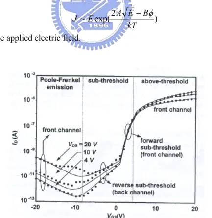
[9]It is believed that the deep states arose from impurities influence the threshold voltage and subthreshold behavior, while the tail states caused by disorder affect the performance when the TFT is switches on [11]. For a-Si TFTs, four regimes of operation can be identified: above-threshold, forward subthreshold, reverse subthreshold, and Poole-Frenkel emission. However, the reverse subthreshold regime is usually absent for OTFT.
Above-Threshold & Forward Sub-threshold Region
In the above-threshold regime, the Fermi level enters the tail states of the valence band. The carriers trapped in tail states play a more important role than those trapped in interface states due to the exponential increase of tail stats. In contrast, in the
sub-threshold regime, the Fermi level moves into the middle gap close to its intrinsic level. So, most of the induced carriers fill the deep localized states in the pentacene bandgap and the interface states at the pentacene/insulator interfaces.
Poole-Frenkle Emission
While the molecules cannot form a perfect crystal leading to a unity energy level, some localized levels are occurred. The carriers have to overcome the discrepancy of each level to hop between molecules [8]. The barrier arising from the disparity of energy level can be lowered by an applied electric field. Consequently, the mobile carriers are produced by Poole-Frenkel field-enhanced thermionic emission at the gate/drain overlap region.
The Poole-Frenkel region is lowered the barrier by an applied field, and a current density can be expressed by
) 2 exp( ~ kT B E A E J − φ
where E is the applied electric field.
Figure 2. 4 The plot of drain current as a function of gate voltage shows four regimes of operation. [9]
2.2 Organic Conductors
2.2-1 Conduction Mechanism
In the late 1970s, the first conducting polymer, doped polyacetylene, was discovered by Heeger, MacDiarmid and Shirakawa. Doped polymers reach conductivities of 105 S/cm, which is much better than that of 10-5 S/cm in the general polymers [2]. It is a challenge to gain insight into the conduction mechanism.
Figure 2. 5 Molecular structures of common p-type organic semiconductors [3].
Schön, Kloc and Batlogg have performed space-charge-limited-current measurements on pentacene crystals [12]. The observed charge transport behavior was, at low temperatures, described as band like transport, which crosses over, at high temperatures, to a hopping mechanism.
Band Transport [3] [12]
At low temperatures, coherent band transport of delocalized carriers is the prevalent mechanism in single crystals of pentacene. In the case, carriers move as highly delocalized plan waves in wide bands. But the lattice vibration could disintegrate the perfect plan waves in periodicity, resulting in interaction between the carriers and lattice atoms. The “bandwidth” decreases with increasing temperature due to coupling with phonons (lattice vibration) to scatter the carriers.
Hopping [3] [12]
At higher temperatures, the strong electron-phonon coupling directs to another mechanism. Because the interplay between carriers and intermolecular vibrations leading to the charge localization, it forms a “lattice polaron”. Consequently, the incoherent hopping motion would be improved by thermal activation. The charge carrier has a certain probability to migrate to its neighboring molecules by either energetically vertical hopping or horizontal tunneling.
Anisotropy
The pentacene molecules within the a-b plane are arranged in a herringbone stacking as shown in Figure 2. 7. Schön et al. [12] also have found that the conductivity of pentacene single crystals is strongly anisotropic.
Although an even higher mobility of 3.2 cm2/Vsec has been obtained for the transport path along the d direction, it is noticeable that the charge transport mechanism in all directions is the same, even the direction perpendicular to the a-b plane (c’ axis).
Figure 2. 7 Hole mobility within the a-b plane of pentacene single crystals at room
temperature. The d direction is the high-mobility direction for hole transport. [12]
2.2-2 Crystal Structure
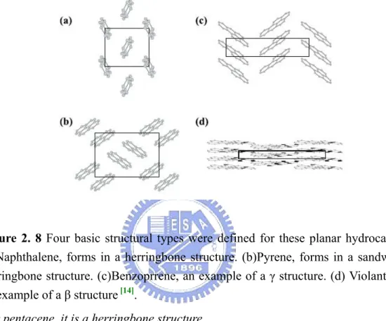
Gautam and Gavezzotti have studied on a lot of planar aromatic hydrocarbons [14]. There are four basic structures recognized as shown in Figure 2. 8. The basis used to distinguish between these four is the length of the shortest axis and the angle between the molecules. For example, the longest axis length is a sandwiched herringbone structure.
lattice, resembling the close-packed structure of inorganic crystals. For disk shaped molecule, it tends to form in β structure, while elongated one prefers to crystallize in herringbone stacking. But, structure prediction is still difficult due to polymorphism.
Figure 2. 8 Four basic structural types were defined for these planar hydrocarbons.
(a)Naphthalene, forms in a herringbone structure. (b)Pyrene, forms in a sandwiched herringbone structure. (c)Benzoprrene, an example of a γ structure. (d) Violanthrene, an example of a β structure [14].
For pentacene, it is a herringbone structure.
2.3 Pentacene
Figure 2. 9 Lewis structure of pentacene.
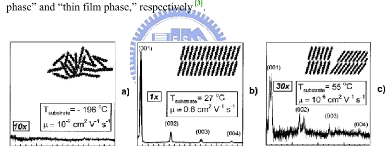
The first identification of pentacene structure was performed by Campbell and coworkers in 1961 [15], with a unit cell of dimension a=7.93, b=6.14, c=16.03Å, α = 101.9°, β = 112.6°, γ=85.8°, and a d-spacing of 14.4Å. Since 1990s, pentacene has been frequently used in TFTs. A new d-spacing was recognized to be 15.4Å. The two observed d(001) values of 14.4 and 15.4Å are commonly referred to as the “bulk phase” and “thin film phase,” respectively [3].
Figure 2. 10 X-ray patterns, schematic structural order, field effect mobility
corresponding to 3 substrate temperatures.[3]
It is believed that large π-conjugation length along the long axis of molecules and close packing along the short axis are two key conditions for high mobility. As shown in Figure 2. 10 (a), amorphous pentacene produced at -196℃ is practically insulating due to the fact that the overlap of the molecular orbitals is very limited. However, when the substrate temperature rises, the high order is formed, and the mobility is better than the case of (a).
From the (b) and (c), we have to distinguish between the “thin film phase” and “bulk phase” of pentacene. Although the temperature is higher than RT, another phase is started growing, the mobility of this mixture is very low, possibly due to the high defect arising from the phase boundaries.
Actually, at least four polymorphs of pentacene are present, characterizing by d-spacing of 14.1, 14.5, 15.0, and 15.4Å [16] [17]. Typically two, 14.5 and 15.4Å, are the “thin film phase” and “bulk phase,” respectively. They have been reported to depend on the film thickness and the substrate temperature during deposition [4]. The former is usually grown at RT, while the latter is presented above a critical thickness and at a higher substrate temperature. The uncommon two, 14.1 and 15.0Å, is strongly depending on what type of substrates is employed: ex. Kapton, a commercial polyimide.
Finally, purity of the pentacene is also important. For example, iodine-doped pentacene is a p-type material, but alkaline metal-doped pentacene is an n-type one [3].
Figure 2. 11 Common impurity in pentacene. Left: 6,13-dihydropentacene. Right:
2.4 The Growth of Thin Film
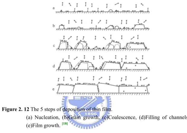
2.4-1 The Mechanism of Deposition of Thin-Film
[18]Traditionally in inorganic system, the deposition of thin film can be divided into several parts as follows:
Figure 2. 12 The 5 steps of deposition of thin film.
(a) Nucleation, (b)Grain growth, (c)Coalescence, (d)Filling of channels, (e)Film growth. [18]
Nucleation
Firstly, when the energetic molecules pass through the boundary layer, most parts of them have to stay a sufficient period of time to diffuse. The energy of these molecules is consumed in the horizontal direction until they are adsorbed physically by the surface, but the energy in the vertical direction is still retained. Subsequently, the adatoms is likely to release condensation heat to form a stable cluster chemically, or to desorb into vapor phase.
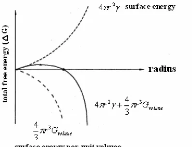
If the adatoms can form a stable cluster, the total free energy has to be negative. From the Figure 2. 13, at the beginning of radius enlarging, the total free energy presents a positive slope, which is unfavorable for grain growth. However, as long as
the radius larger than a critical value, the total free energy has a negative slope, which is favorable for grain growth [19].
The model described above does not involve into interface between grains and substrates. For the heterogeneous nucleation, it is not proper to assume the grain shape is spherical. The wetting angle should be considered.
Figure 2. 13 The relationship of free energy to radius of grains.
γ is the surface energy per unit of the clusters, and Gvolume is the surface energy per
unit volume. [19]
Figure 2. 14 Wetting angle in the heterogeneous nucleation.[19]
Grain Growth and Coalescence
After clusters possessing a critical radius, the grain growth (step b) starts. Unlike the previous step, the growing grains can catch the molecules from vapor phase
directly, not localized the adatoms.
When the individual grain is large enough to contact each other, coalescence occurs. In order to decrease the surface energy, inter diffusion between each grain proceed to fill the neck.
However, if the crystal structure of both grains is not identical, one is <111> and the other is <110> for instance, it has to be through recrystallization, stabilizing the energy states of new grains [18].
2.4-2 Fractal –Mound Growth of Pentacene Film
The mechanism of pentacene growth on SiO2 substrate has been studied [20]. The
model of Diffusion-Limited Aggregation (DLA) governs the lateral growth, while the Ehrlich-Schwoebel barrier effect disrupts the desired epitaxial growth for the subsequent layers, leading to mound growth.
Diffusion-Limited Aggregation
With sufficiently low nucleation density, the terraces of pentacene islands have a fractal dimension of 1.6~1.7, agreeing a lateral DLA shape [1]. After the molecule sticks to the edge, the transient diffusion at the step edges might occur immediately and continue until it finds a suitable site.
Ehrlich-Schwoebel Barrier
Step-flow growth is often under the assumption that adatoms bond to ascending and descending steps with equal rates. However, an excess energy barrier to migration over descending steps exists, which produces an adatom “uphill current.” For example, if a terrace is larger than its upper neighbor, it will receive more adatoms flux which preferentially attach to the ascending step [21][22].
From the left of Figure 2. 17, the subsequent layer does not start forming until the first one completes. It denotes a layer-by-layer mechanism as opposed to the mound growth.
Figure 2. 15 Coverage-dependent fractal dimension of single-molecular-layer pentacene islands on cyclohexane-saturated Si(001). [1]
Figure 2. 16 The cross section of a monatomic step in a surface and the hypothetical potential associated with the diffusion of an atom over such a surface.[22]
Figure 2. 17 (Left) A simulated surface without the presence of the Ehrlich-
Schwoebel barrier, (Meddle)A simulated surface approaching real situation, (Right) Fourier transform of a typical pentacene surface. Ring structure is a sign of mound growth. [20]
2.5 X-Ray Diffraction Analysis
2.5-1 The Scherrer Equation
[23] [24]θ β λ cos K Lhkl =
where Lhkl is the average of the crystallite size perpendicular to the planes (h k l), β is
the breadth at intensity of half-maximum in radians, and K is a constant commonly assigned a value of unity. The normal form can be expressed the reflection breadth in δs units as follows: s K Lhkl δ δθ λ θ 1 ] / cos 2 [ ≈ = , where s=2(sinθ)/λ
2.5-2 Distortion of the First and Second Kinds
[24]Hosemann postulates that a real crystal is subject to two distortions: first and second kinds, as shown in Figure 2. 18.
Figure 2. 18 Optical diffraction models of lattice with 1-D distortions (a) of the first kind, and (b) of the second kind. [24]
Distortion of First Kind (gI)
If a lattice is influenced only by the distortion of first kind, the long-range periodicity is preserved. It means that the distortion is displacements of the structural elements, such as atoms or motifs, from the ideal lattice points.
) 4 exp( ) (m 2g2m2 D = − π I ,
the effect of distortion (I) on the diffraction patterns will be indistinguishable from the effect of thermal vibration. Thus, the distortion (I) is regarded as frozen-in thermal displacements, resulting in a falling off of the intensity of a set of reflections with increasing order, m. However, it makes no broadening.
Distortion of Second Kind (gII)
If a lattice possesses the distortion of second kind, the long-range periodicity is lost. It means that each lattice point varying in position only relates to its neighboring ones rather than to the ideal sites. Compared to the distortion (I), the distortion (II) results in both a decrease of intensity and an increase of breadth with higher reflection order m.
2.5-3 Paracrystal Theory
[24]For semicrystalline systems, the Scherrer equation is used to describe the relationship of the breadth to crystallite size. However, the breadth is always broader than the expectation of crystallite-size effect due to the distortion of second kind. Thus, the Sherrer equation should be replaced by:
2 4 4 4 2 2 2 2 ( ) ( ) 1 ) ( hkl II hkl II c d m g L s s s δ δ π δ = + = + , where λ θδθ δs= 2cos ,
which is valid if is much smaller than unity, and the broadening profiles are Gaussian shape exhibiting the polydispersity is small.
2 2 2
2π gIIm
In this equation, (δs) is the total broadening excluding instrumental broadening, λ is the X-ray wavelength, δθ is the breadth expressed in radians, (δs)c and (δs)II is the
broadening from the crystal size and lattice distortion of second kind, respectively. As todhkl , it is the spacing of (hkl) planes from Bragg’s law.
CHAPTER 3
Experimental Methods
3.1 Device Fabrication
3.1-1 Preparation of Substrates
In our work, heavily doped n-type silicon wafer with thermal SiO2 was chosen
as the device substrate. The 200nm-thick SiO2 grown on the polished side of the
wafer was served as the gate dielectric, and the Al metallic layer deposited on the other side formed the gate contact.
Subsequently, the SiO2 surface was cleaned with “half RCA procedure” which
means de-ionic water, H2SO4-H2O2 solution (3:1 by volume), de-ionic water, in order.
The details were illustrated in Figure 3.1.
Figure 3.1 The procedure of substrate cleaning.
Step 1: Place the wafers on the Teflon carrier, and pre-rinse the wafers in the D.I. water for 5 minutes.
Step 2: Submerge the carrier with wafers in the H2SO4-H2O2(3:1) solution, and keep the temperature at 85℃ for 20 minutes.
Step 3: Remove the carrier from the acidic bath, and rinse it again in the D.I. water beaker for 5 minutes.
3.1-2 Surface Treatment
Si CH3 CH3 CH3 Si H3C N CH3 CH3 H HMDS C CH3 C H2 n PαMSFigure 3.2 The chemical formula of 1,1,1,3,3,3- hexamethyldisilazane and poly(α-methylstyrene).
After the substrate cleaning, we tried 3 types of surface treatments. Two chemicals,1,1,1,3,3,3- hexamethyldisilazane (HMDS)and poly(α- methylstyrene) (P MS) , were spread onto the SiO2 surface, and bare one was used as a reference.
For the two modifications, one was evaporated in the HMDS oven at 150℃, while the other was spin coated with 0.3wt% solution of PαMS in toluene. Further postbaking was not applied to the HMDS -treated substrate to prevent any change of surface properties. On the contrary, postbaking was done for the PαMS-treated one at 80℃ for 1 hour to remove residual solvent. The HMDS film was too skinny to be estimated, and the P MS film was about 8-nm-thick.
Si CH3 CH3 CH3 Si H3C N CH3 3 H Si Si Si OH OH OH (1) CH Si CH3 CH3 CH3 Si H3C N CH3 CH3 H O H H Si 3 CH3 CH3 Si H3C N CH3 CH3 H Si Si Si OH O H OH (2) CH Si CH3 CH3 CH3 Si H3C N CH3 CH3 H H OH
CH3 CH3 Si H3C Si Si O (6) CH3 CH3 O Si H3C Si O CH3 CH3 Si H3C Si CH3 CH3 CH3 Si H3C O CH3 CH3
Figure 3.3 A probable mechanism for the chemical reaction of HMDS.
HMDS can change the OH-terminated SiO2 to a (CH3)3-Si-terminated one.
3.1-3 Growth of Thin Film and Electrodes
Next, 99.9% pentacene purchased from Fluka without additional purification, was employed as the active layer. It was sublimated by thermal coater under a back pressure below 1.1×10⁻⁶ torr. The substrate could be heated from 17℃ to 90℃, and measured with an Al-Cr thermocouple. As for deposition rate, it was controlled at a
Si 3 CH3 CH3 Si H3C NH2 CH3 Si Si Si OH O OH (3) CH CH3 CH3 CH3 Si H3C NH2 HO H Si CH3 CH3 CH3 Si H3C NH2 CH3 CH3 Si Si Si OH O O H (4) CH3 CH3 Si H3C NH2 OH H CH3 CH3 CH3 Si H3C NH3 CH3 Si Si Si OH O O Si H3C (5) Si CH3 CH3 CH3 Si H3C O CH3 CH3 CH3 CH3 Si H3C OH Si CH3 CH3 CH3 HO
rate of 0.5 Å/sec by a quartz oscillator during the thin-film formation. A shutter allowed the stable pentacene flux to pass until the total thickness approached 60 nm.
In order to match the work function of pentacene, whose HOMO is about 5.1eV, gold is appropriate for pentacene-based OTFTs as source/drain electrodes. Accordingly, 35-nm-thick Au, as top contacts, was deposited at a rate of 2~3 Å/sec through a shadow mask under 3×10⁻⁶ torr. The channel width (W) was 2000μm for all devices in this study, and channel lengths (L) were varied as 75, 95, 130, 160μm.
n++Si Gate SiO2 dielectric
by half RCA procedure. To clean substrates
n++Si Gate SiO2 dielectric
PαMS or HMDS
to modify the bare SiO2
To apply chemicals
n++Si Gate SiO2 dielectric
Pentacene
at various temperature. on the modified substrates To sublimate pentacene n++Si Gate SiO2 dielectric drain source Pentacene To evaporate Au as top contacts.
3.2 Device Measurement
Electrical characterization was taken in a light-isolated probe station, connected to a semiconductor parameter analyzer (Keithley 4200) at room temperature in atmosphere.
For pentacene-based devices, a negative bias of gate voltage was applied to accumulate holes in the p-type active layer. In the ID-VD measurement, the drain bias
was swept from 0 to -60 Volts and the gate voltage step were 0, -15, -30, -45, -60 Volts, respectively. In the ID-VG measurement, the gate bias ranged from +20 to -60
Volts, and the drain voltage step were 0, -15, -30, -45, and -60 Volts. However, it could be modulated in special case.
3.3 Instrument and Chemicals
Name Type Specification
Vacuum Oven Yield Engineering Systems, YES - 5
Spin coater Chemat Technology, KW-4A
Thermal coater ULVAC, CRTM-6000
Semiconductor parameter analyzer Keithley 4200
AFM DI3100
XRD M18 XHF, MacScience
Contact angle Kruss Universal Surface Tester, GH100 Pentacene Fluka
CHAPTER 4
Results and Discussions-
Electrical properties vs. Morphology
4.1 Review of Prior Arts
At the beginning, we will introduce a similar research about the effect of substrate temperature on the device properties. Jiyoul Lee et al. [25] has reported that the grain size of the pentacene enlarges with the substrate temperature accompanies by a phase transition. Nevertheless, the hole mobility is not improved much by varying the temperature as expected. In addition, Lee has observed that the XRD peak intensities of large grains were much lower than those with small grains. It seems to suggest that the large grains may contain more defects or disordering. Consequently, they have attributed the little fluctuation of mobility to a higher density of traps at higher temperature.
Although a similar research has been done, the result cannot distinguish the thin-film phase and bulk phase, which are affected by the substrate temperature simultaneously. Otherwise, different crystal systems may have different absorption coefficient of X-ray[23] [24], which means the XRD intensities may not compare with each other simply. In other words, lower intensity is not necessary to stand for less ordering. It is probably to make the XRD spectra to become invalid in the study. In contrast, we have separated the two factors, the enlargement of grain size and the phase transition, successfully. That will make the XRD more significant for the conclusion.
4.2 A Preparation by Making Use of SiO
2Substrate
Part A: Morphology Evolution
4.2-1 The Relationship between the Deposition Temperature to the
Grain Size
Figure 4. 1 AFM images of 60-nm-thick pentacene deposited at a fixed flux rate of
0.5Å/sec on a 200-nm-thick SiO2 substrate without surface treatment at various
deposition temperatures. The focus position is between the source/drain electrodes. (A)T =17℃, R=10.273nm. (B) T =30℃, R=9.610nm. (C) T =50℃, R=8.976nm. (D) T =70℃, R=6.680nm. (E) T =90℃, R=7.105nm. (F) T =110℃, R=8.570nm.
All the images are 3×3μm2 except the bigger two which are 5×5μm2. (R: roughness presented by root-mean-square form)
The AFM images of Figure 4. 1 display the surface morphology of 60-nm-thick pentacene deposited on bare SiO2 substrate at 17℃, 30℃, 50℃, 70℃, 90℃, and
110℃ respectively. The rms surface roughness of each film varied in the range of 6-10nm. Note that it merely forms stable film until the substrate is heated at 120℃ which is probably due to the equal rate of adsorption and desorption.
According to the evolution of morphology, the grains show a progress enlargement conspicuously as the substrate temperature goes up. Since the grain boundaries behave as a barrier against carrier hopping [11], it is believed that larger grain sizes, which mean less grain boundaries, should be more conductive.
Part B: I-V Characteristics
4.2-2 The Mobility Calculation
In the following section, we will extract the mobility (μ) from the saturation regime of the field-effect transistor model.
At higher VD, which means –VD > –(VG-VT), ID tends to saturate, and is
approximately determined by the equation:
2 ) ( 2 G T i D V V L WC I = μ − => ( ) 2 G T i D V V L WC I = μ −
We have obtained μ from the maximum tangent in the plot of ID versus VG,
i.e. slope= L
WCi
2 μ
. It is important to note that this equation is only valid when μ is constant. Thus, despite of the most widespread use, it should be treated as an approximate value.
4.2-3 The Transfer Characteristics
the OTFTs, which were fabricated at
-60 -40 -20
0
20
40
60
80
10
-1110
-1010
-910
-810
-710
-610
-510
-40.000
0.004
0.008
0.012
0.016
0.020
-I
D
(A)
17oC 50oC 90oCVG(V)
[-I
D
(A)]
1/ 2Figure 4. 2 The transfer characteristics of
various deposition temperatures with bare SiO2 substrate, obtained under VD=-60V.
10 30 50 70 90 0.1 0.2 0.3 0.4 0.5 mobili ty (cm 2 /Vse c) Temperature(oC)
Figure 4. 3 The results of the mobility calculation from the saturation regime of the modeling of field-effect transistor. Circle: the average obtained from the maximum tangent in the plot of ID versus VG.
The relationship of the hole mobility to deposition temperature is revealed in Figure 4. 3
Figure 4. 2 T
√-ID) plots in Figure 4. 2 exhibits two gradations at
higher tem
G T
art C: Crystal Structure
. For the device without surface treatment, the average mobility goes up from 0.17 to 0.41 cm2/Vsec by deposition temperature elevated. It demonstrates that the higher the temperature is, the better the device performance becomes.
However, the corresponding transfer characteristics of the OTFTs as shown in present a threshold voltage (V ) shift which moves toward a more positive bias with the higher deposition temperature. The early turn on at higher temperature may result from the higher trap density [25] or more dipoles in the insulator/pentacene interface.
In addition, the slop of the (
perature seriously: a slow slope nearby the turn on point while a steep one away from it. It is well known that the mobility in some OTFTs is gate bias dependent. Strictly speaking, it is more relative to the (V -V ). If we extract each mobility from the secant to obtain the average value, the device prepared at 90℃ will not perform outstandingly as before. Hence, the mobility estimated from the FET model might be overestimated for the device fabricated at high temperature.
P
4.2-4 The Phase Transition
ctra of pentacene structures on various conditions. Figure 4. 4 illustrates the XRD spe
There are two sets of diffraction peaks in the spectra: (00l’) is for 2θ of a multiple of 5.7 degrees, and (00l) is for a multiple of 6.2 degrees.
By Bragg’s law:2dsinθ =nλ , the set, (00l’), is determined with vertical periodicity of 15.4Å, while the other set, (00l), reveals the d-spacing of 14.4Å. The set of (00l’) has been identified as “thin-film phase”, and (00l) is so-called “bulk phase.”
[6] [25]
In terms of the full widths at half maximum, the films deposited through substrate heating show slightly higher crystalline quality than the ones deposited at RT. We ascribe the formation of higher order to annealing during pentacene deposition. However, as indicated by the rectangle of Figure 4. 4 not only thin-film phase but also bulk phase grows with deposition temperature. Growth of both phases might bring about incoherence between phase boundaries.
5
10
15
20
25
(004 ) (004 ') (003 ) (003 ') (002 ) (002 ') (001 ) (001 ') 90oC 70oC 50oC 17oC log(In tens ity) (a.u.)2
θ(deg.)
Figure 4. 4 X-ray diffractograms using CuKα (λ=1.54 Å). The samples were prepared
by the pentacene deposited at a fixed flux rate of 0.5Å/sec on a 200-nm-thick SiO2
substrate at various deposition temperatures.
Note that the fatty peak at 2θ of 13.5 degrees belongs to SiO2, not to pentacene.
4.2-5 Conclusion
In summary, we have prepared pentacene-based TFTs, which were deposited on SiO2 gate dielectrics at various substrate temperatures. The AFM images show that
more grain boundaries could hamper carrier transport.
However, the XRD spectra indicate that an incoherence between two phases occurs in spite of the high order growth in thin film phase. Even if we only utilize substrate heating to enlarge grains, other factors would disturb this effect. Too many variables would make the analysis less powerful.
Furthermore, the VT shift is a thorny problem in mobility estimation especially.
The outcome, the better performance due to the higher deposition temperature, seems to jump to a conclusion.
In order to make sense of the XRD spectra and to reduce the VT shift, it is
necessary to inhibit the phase transition and trap density at higher temperature. There is a possible method to come to this objective: to modify the substrates [26]. It might relax the strain of phase transition and simultaneously alter the interfacial states.
In the following sections, we have tried two types of surface treatments: 1,1,1,3,3,3- hexamethyldisilazane [27] and poly(α- methylstyrene) [28]. We attempt to find out the relationship of electrical properties to grains without disturbance such as VT shift and phase transition.
Si CH3 CH3 CH3 Si H3C N CH3 CH3 H HMDS C CH3 C H2 n PαMS
4.3 The Relationship of the Mobility to the Grains
4.3-1 The Transfer Characteristics without V
TShift
-60
-40
-20
0
20
0.000
0.004
0.008
0.012
0.016
0.020
-60
-40
-20
0
20
10
-1110
-1010
-910
-810
-710
-610
-510
-4[-I
D
(A)]
1/2
17OC 50OC 70OC 90OC(a)
-I
D
(A)
VG(V)
-60
-40
-20
0
20
10
-1110
-1010
-910
-810
-710
-610
-510
-40.000
0.004
0.008
0.012
0.016
0.020
(b)
-I
D
(A)
[-I
D
(A)]
1/2
17OC 50OC 70OC 90OCVG(V)
Figure 4. 5 The transfer characteristics of the OTFTs, which were fabricated at
various deposition temperatures with (a) HMDS-treated substrate, (b) PαMS-treated substrate, obtained under VD=-60V.
Compared with Figure 4. 2, Figure 4. 5 illustrates that the VT shift is not clear,
and the devices turn on at negative bias, not at positive bias as before. The VT shift as
shown in Figure 4. 5 is less than 10V, which would solve a basal problem in estimating mobility. It is a good beginning to study the relationship of mobility to grains in the next sections.
But, why the surface treatments work?
It is notice that the contact angle of bare substrates drops dramatically with decreasing temperature. In contrast, however, the contact angles of the two treated substrates are nearly identical. This is likely the reason that VT shift could be wiped
off by surface treatments.
Note that the turn on voltage of PαMS-treated devices center on -5V except for the one prepared at 90℃. It has turned on at a more negative bias than the others. This obvious shift might be due to the glass transition of PαMS, which should be regarded as another modified material.
On the other hand, the devices with surface treatments have turned on at negative bias, whereas the bare ones have actuated at positive bias. This part will be discussed in the section 4.5.
Surface Treatment Substrate Temperature (oC) Contact Angle (H
2O) 20 49.8 Bare 90 60.0 20 67.5 HMDS 90 67.0 20 84.0 PαMS 80 82.8
4.3-2 Inhibition of Phase Transition
5
10
15
20
25
(004 ) (004 ') (003 ) (003 ') (002 ) (002 ') (001 ) (001 ') 70oC 50oC 90oC 17oClog(
Int
en
sit
y)
(a.u.)
2
θ(deg.)
5
10
15
20
25
(004 ) (003 ) (004 ') (003 ') (002 ) (002 ') log( In tensit y) (a .u. )2
θ(deg.)
90oC 50oC Figure 4. rate of0.5Å/sec on a (top) HMDS-treated substrate, (bottom) PαMS-treated substrate at various deposition temperatures.
6 XRD spectra of 60-nm-thick pentacene deposited at a fixed flux 30oC 17oC (001 ) (001 ') Inte nsity 110oC
Coherence of Phases
he rectangle of Figure 4. 6, the crystal progressively evolves into
Molecular Orientation
As indicated by t
bulk phase (00l) on the HMDS-treated substrates, whereas it maintains thin-film phase (00l’) with the higher substrate temperature on PαMS-treated substrates. It is believed that the phase evolution is related to the strain relaxation of initially strained thin-film phase. This figure proves that the phase transition has been repressed by the PαMS treatment, probably due to the strain release by polymer chains.
, the pentacene crystal on the treated substrates demonstrates a str
should make the Ehrlich-Schwoebel barri
Intensity
In the XRD patterns
ong Bragg reflection at 19.2°, which is absent in the case of bare substrates. This peak is estimated to be an unresolved doublet arising from (110) and (111) reflections with a d-spacing of ~2.5Å [29]. The appearance of (110) and (111) reflections infer that it exists flat-lying molecules on the substrate surface which is likely to make better adhesion between inorganic/organic interface.
Additionally, the flat-lying molecules
er lower. If the molecules deposit without E-S effect, the film growth is close to layer-by-layer mechanism.
e HMDS-treated patterns, the intensity becomes stronger with increasing temp
For th
erature, which is similar to the untreated ones. For the PαMS-treated patterns, however, it is an opposite case. The film deposited at RT shows better reflections than the ones deposited through substrate heating.
4.3-3 Morphology Evolution
0.5Å/sec on a 200-nm-thick SiO2 substrate with HMDS treatment at various
. (B) T =30℃, R=9.630nm (C) T =50℃, R=12.496nm. ) T =70℃, R=9.325nm. (E)T =90℃, R=8.788nm.
Figure 4. 7 AFM images of 60-nm-thick pentacene deposited at a fixed flux rate
=
deposition temperature. (A)T =17℃, R=10.672nm (D
g 2 e o which are 5×5μm2.
All the ima es are 3×3μm except th gray (bigger) tw (R: roughness presented by root-mean-square form)
Figure 4. 8 AFM images of 60-nm-thick pentacene deposited at a fixed flux rate
=0.5Å/sec on a 200-nm-thick SiO2 substrate with PαMS treatment at various
. (B) T =30℃, R=8.970nm. (C) T =50℃, R=10.102nm. ) T =70℃, R=9.071nm. (E) T =90℃, R=10.211nm.
Evolution of Grain Size
deposition temperature. (A)T =17℃, R=9.027nm (D
mages of 60-nm-thick pentacene with HMDS-treated substrates, while
ference in grain gaps between
ure favors pentacene to diffuse on the Figure 4. 7 is the first group of AFM i
Figure 4. 8 is the second group with PαMS-treated ones. Similar to bare substrates, HMDS-treated samples also display an obvious enlargement with deposition temperature. But for the PαMS-treated samples, the grain sizes grow in the beginning, slow down at 70℃, and finally become smaller at 90℃. It also shows a pronounced morphological dif Figure 4. 8(E) and the others.
surfa
volution of Grain Shape
ce and to nucleate on fewer sites. But, a large grain should be formed by lower rate of nucleation and higher rate of lateral growth. The glass transition temperature (Tg) at atmosphere of our PαMS is 85℃, but it should be lower than 85℃ under high vacuum. Above the Tg point, molecule chains could obtain more energy which would raise the nucleus number, and diminish grain size. Accordingly, this morphological difference probably results from the violent molecular motion of PαMS at 90℃.
E
Apart from the grain size, it is noticeable that the dendrite-shaped grains disappear at the medium temperature on the PαMS-treated substrates. It also disappears at the high temperature on the bare substrates. The dendrites are independent of the crystal phase, but dependent on deposition temperature.
The model of Diffusion-Limited Aggregation (DLA) is widely used to explain the g
law of heat conduction (Fourier’s law),
rowth of dendrites [30]. DLA is the process whereby particles undergo a random walk (Brownian motion) to push the molecules approach the growing clusters. Once the molecules stick to the cluster, the transient diffusion at the step edges occurs immediately.
From the
T k q=− ∇ ,
the direction of heat flow depends on the temperature gradient at the interface. When the films grow into a supercooled liquid, the interface is unstable. Suppose a small protrusion forms at the interface, the negative temperature gradient in the liquid becomes more negative. Therefore, heat is removed more effectively from the protrusion than from the surrounding regions. That will allow the arms to grow preferentially, and hinder the neighboring arms from forming [19] [31].
Review 4.1 The temperature distribution for the dendrite growth.
[From Chalmers, B., trans. AIME, 200 519 (1954)] [19]
To return to our system, when the pentacene molecules freeze, the latent heat will be released at the vapor/solid interface. If the latent heat is not removed immediately, it will result in the temperature distribution such as Review 4.1. The dendrites are controlled by the rate at which the latent heat can be removed from the vapor/solid interface, and if the vapor temperature reach a critical supercooling. That is why the dendrites disappear at the relatively high deposition temperature, which is influenced by the thermal property of substrates simultaneously.
Evolution of Initial Layers

![Figure 1.2 Evolution of hole mobility for the most common p-type organic semiconductors [3]](https://thumb-ap.123doks.com/thumbv2/9libinfo/8064912.163153/17.892.275.676.124.417/figure-evolution-hole-mobility-common-type-organic-semiconductors.webp)
![Figure 2. 3 Density states in the band gap of intrinsic a-Si:H. [10]](https://thumb-ap.123doks.com/thumbv2/9libinfo/8064912.163153/22.892.191.698.295.707/figure-density-states-band-gap-intrinsic-si-h.webp)
![Figure 2. 6 Carrier transport in the organic semiconductors. [13]](https://thumb-ap.123doks.com/thumbv2/9libinfo/8064912.163153/25.892.160.787.521.898/figure-carrier-transport-organic-semiconductors.webp)