以效能為導向之輸入輸出緩衝器區塊與核心單元擺置的覆晶式設計
45
0
0
全文
(2) 以效能為導向之輸入輸出緩衝器區塊與核心單 元擺置的覆晶式設計 Performance Driven I/O Buffer Block Planning with Core Placement in Flip-Chip Design 研究生﹕張加易. Student﹕Chia-Yi Chang. 指導教授﹕陳宏明 博士. Advisor﹕Prof. Hung-Ming Chen. 國立交通大學 電子工程學系 電子研究所碩士班 碩士論文. A Thesis Submitted to Department of Electronics Engineering & Institute of Electronics College of Electrical Engineering and Computer Science National Chiao Tung University in Partial Fulfillment of Requirements for the Degree of Master of Science in Electronics Engineering June 2005 Hsinchu, Taiwan, Republic of China 中華民國九十四年六月.
(3) 以效能為導向之輸入輸出緩衝器區塊與核心單元擺置 的覆晶式設計 學生:張加易. 指導教授:陳宏明 博士 國立交通大學. 電子工程學系 摘. 電子研究所. 碩士班. 要. 隨著製程的進步,越來越多的電路可以整合進去單一的晶片裡面,這 同時也代表在現今的設計裡面需要越來越多的輸出輸入單元。覆晶式 設計跟傳統的週遭式焊接線設計相比,它更適合需要大量輸出輸入的 設計,在這篇論文裡面我們提出了一個覆晶式設計的輸入輸出緩衝器 區塊與核心單元擺置的演算法,可針對面積、接線長度、信號的不對 稱做優化,這個演算法可以銜接既有的擺置方法,將原來的擺置做成 覆晶式的設計,實驗數據顯示我們的方法跟傳統週遭式焊接線設計有 更好的效能,特別是在擁有更多的輸出輸入單元的設計上。.
(4) Performance Driven I/O Buffer Block Planning with Core Placement in Flip-Chip Design. Student﹕Chia-Yi Chang. Advisor﹕Prof. Hung-Ming Chen. Department of Electronics Engineering & Institute of Electronics National Chiao Tung University. Abstract. As silicon technology scales, we can integrate more and more circuits on a single chip, which means more I/Os are needed in modern designs. The flip-chip design is better than the typical peripheral wire-bond design in the increase in I/O count. In this thesis, we develop an I/O buffer block placer algorithm in area, wirelength and signal skew optimization for flip-chip design. We can add this step to an existing design flow to convert the initial peripheral wire-bond I/O design to area array I/O design. Experimental results have shown that our algorithm has better performance compared with peripheral design in high I/O count circuits..
(5) 誌謝 這篇論文得以順利完成要感謝周遭許多人。 感謝我的指導教授陳宏明博士,老師不僅在專業上給予學生指 導,連生活上的小細節都很關心學生,跟學生們打成一片,一點都沒 有老師的架子,由衷感謝老師的幫忙與指導,讓我可以順利完成這篇 論文。 感謝實驗室的同學們幫助我解決課業上及論文的問題,大家樂於 相互討論很有一個團隊的感覺,還有學弟們讓實驗室裡時時充滿歡樂 輕鬆的氣氛。 感謝一些以前的大學同學,讓我的研究所生活多了一些娛樂,吃 飯的時候不會覺得無聊,打球的時候有人陪。 最後感謝我的父母,讓我衣食無缺無憂無慮的完成我的碩士學 位。.
(6) Contents. 1 Introduction 1.1. 1. Organization of this Thesis . . . . . . . . . . . . . . . . . . . . . . . .. 2 Area Array I/O Buffer Block Placement. 3 4. 2.1. I/O Buffer Modeling . . . . . . . . . . . . . . . . . . . . . . . . . . .. 4. 2.2. Force Directed Placement Flow . . . . . . . . . . . . . . . . . . . . .. 6. 2.3. Area Array I/O Buffer Placement Methodology . . . . . . . . . . . .. 8. 2.4. Problem Formulation . . . . . . . . . . . . . . . . . . . . . . . . . . .. 8. 3 The I/O Buffer Block Placer Algorithm. 11. 3.1. Buffer Modeling . . . . . . . . . . . . . . . . . . . . . . . . . . . . . . 12. 3.2. BufBlockPlacer . . . . . . . . . . . . . . . . . . . . . . . . . . . . . . 14 3.2.1. Cell Squeeze . . . . . . . . . . . . . . . . . . . . . . . . . . . . 15. 3.2.2. Local Legalization. 3.2.3. Buffer Merge . . . . . . . . . . . . . . . . . . . . . . . . . . . 18. 3.2.4. The BufBlockPlacer Algorithm . . . . . . . . . . . . . . . . . 19. . . . . . . . . . . . . . . . . . . . . . . . . 16. 3.3. Global Legalization . . . . . . . . . . . . . . . . . . . . . . . . . . . . 19. 3.4. Signal Bump Assignment . . . . . . . . . . . . . . . . . . . . . . . . . 19. iii.
(7) 3.5. Summary of Our Algorithm . . . . . . . . . . . . . . . . . . . . . . . 21. 4 Experimental Results. 25. 5 Conclusion and Future Works. 31. Bibliography. 32. iv.
(8) List of Figures 1.1. Area-array footprint ASIC. The Vdd and Gnd bumps are uniformly distributed across the die with signal bumps in fixed interspersed locations. I/O buffers are associated with some specified signals bump and connected by pad transfer metal.[14] . . . . . . . . . . . . . . . .. 2.1. 2. Annotated photomicrograph of DES IC with I/O buffer blocks grouped at the center of the chip [16]. . . . . . . . . . . . . . . . . . . . . . . .. 5. 2.2. The structure of I/O buffer block and signal pad [16]. . . . . . . . . .. 6. 2.3. The force on a cell A connected with four cells . . . . . . . . . . . . .. 7. 2.4. Intrinsic area-array pad placement and routing flow from [10], and proposed modeling and placement step. . . . . . . . . . . . . . . . . .. 9. 3.1. The flow chart of our buffer block placer algorithm . . . . . . . . . . 12. 3.2. The model of our I/O buffer block . . . . . . . . . . . . . . . . . . . . 13. 3.3. The size of buffer block used in MCNC benchmark struct . . . . . . 14. 3.4. The Squeeze has three direction to squeeze cells right, up and down . 16. 3.5. Moving the cell at the boundary of the net will change wire length of the net . . . . . . . . . . . . . . . . . . . . . . . . . . . . . . . . . . . 16. 3.6. Wave sequentially move cells from min row to max row in the wave zone . . . . . . . . . . . . . . . . . . . . . . . . . . . . . . . . . . . . 18 v.
(9) 3.7. The weight in wave calculate the wire length cost in the operation pull and push . . . . . . . . . . . . . . . . . . . . . . . . . . . . . . . 18. 3.8. The BufferPlacer algorithm . . . . . . . . . . . . . . . . . . . . . . . 20. 3.9. An example for signal bump assignment . . . . . . . . . . . . . . . . 21. 3.10 The initial placement, those rectangles represent cells. . . . . . . . . . 22 3.11 The placement placed with buffer blocks after the execution of BufBlockPlacer, dark rectangles represent buffer blocks and those lines represent the connection of the cells. . . . . . . . . . . . . . . . . . . 23 3.12 A fine tuned placement after the process of Local legalization . . . . . 23 3.13 The final placement after the process of Signal Bump Assignment, those squares over the cells represent signal bumps. . . . . . . . . . . 24 4.1. The placement of struct with peripheral design (from the placer FENG SHUI [21]). . . . . . . . . . . . . . . . . . . . . . . . . . . . . . 28. 4.2. The final result of struct with BufBlockPlacer. . . . . . . . . . . . . . 28. 4.3. The placement of biomed with peripheral design. . . . . . . . . . . . . 29. 4.4. The final result of biomed with BufBlockPlacer. . . . . . . . . . . . . 29. 4.5. The placement of industry2 with peripheral design. . . . . . . . . . . 30. 4.6. The final result of industry2 with BufBlockPlacer. . . . . . . . . . . . 30. vi.
(10) List of Tables 4.1. Number of cells, nets and I/O terminals in some MCNC standard cell placement benchmarks. . . . . . . . . . . . . . . . . . . . . . . . 25. 4.2. Area comparisons between our approach and the peripheral design with the MCNC benchmark. . . . . . . . . . . . . . . . . . . . . . . . 26. 4.3. Wirelength comparisons between our approach and the peripheral design with the MCNC benchmark and the result of signal skew. . . . 26. 4.4. Run time comparisons for our I/O buffer placer with the MCNC benchmark industry2, we adjust the parameter of the weight to make legalization process consider wirelength only or both wirelength and run time. . . . . . . . . . . . . . . . . . . . . . . . . . . . . . . . . . . 27. vii.
(11) Chapter 1 Introduction As silicon technology scales, we can integrate more and more circuits even entire electronic system on a single chip (SoC). Since more circuits are integrated on one single chip, that means more I/Os are needed in modern designs. Many highperformance ICs and microprocessors are built with more I/O connections than in the past [1]. [2] showed the trend in the increase in I/O count and the reduction of die size when the typical peripheral wire-bond design was replaced by the flip-chip design. As a result, the flip-chip design shown in Figure 1.1 is considered a better choice [3,4]. There are some more advantages of flip-chip design: • Minimizes size of electrostatic discharge (ESD) structure for intra-package IO • Improved signal integrity due to power and ground pad structure Since flip-chip design allows I/O buffers to be placed anywhere on the die, we need to focus on the change to better the design and the cost for placing I/O buffer blocks into the design. Many approaches and methodologies have been presented in the literature [5,6,7,8,10], dealing with I/O placement and electrical checking using flip-chip technology. In [9], they utilized flip-chip design to minimize interconnect length which is the major concern in I/O placement. Recently, [14] further consider the building cost of I/O buffer blocks. 1.
(12) Figure 1.1: Area-array footprint ASIC. The Vdd and Gnd bumps are uniformly distributed across the die with signal bumps in fixed interspersed locations. I/O buffers are associated with some specified signals bump and connected by pad transfer metal.[14]. I/O buffers usually come with peripheral circuitry such as testing logic and ESD structure. There is a required minimal spacing between ESD structures and active devices due to the foundry rules [16], forming a clearance region between standard cells and I/O buffer blocks. Once we clustered I/O buffers in one single block, the clearance region is shared. In addition, the design cost for power routing to the. 2.
(13) buffer block is reduced as well. Comparing to the approaches which place I/O buffers in greedy ways [7,10], the design cost can be apparently reduced. Therefore, the tradeoff between performance and cost in I/O buffer placement should be seriously considered. For most flip-chip designs, like microprocessors, there are a large number of input/output pins used as data bus. For such designs, we must control the signal skew problem carefully. In other words, we have to make sure that signals arrive in the core simultaneously. This can be achieved by adjust the positions of bump balls. input/output buffer blocks and cells. In this thesis, we study the problem of I/O buffer placement for flip-chip design. We built up a simple model for I/O buffer block and propose a placement algorithm to minimize interconnection length and reduce signal skew.. 1.1. Organization of this Thesis. The remainder of this thesis is organized as follows. Chapter 2 describes the I/O buffer placement considerations, our model for I/O buffer block, force-directed placement flow and problem formulation. Chapter 3 presents our four-stage algorithm with a legalization, a numerical analysis method, and some heuristic methods. Chapter 4 shows the experimental results. Chapter 5 presents the conclusion and future works.. 3.
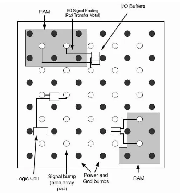
(14) Chapter 2 Area Array I/O Buffer Block Placement Flip-chip technology allows our design to be built with many more I/O connections and power bumps than in the past. As a result, the design will counter many other problems such as long interconnection path [9] and hot-spot problem [15]. While performing area array I/O buffer block placement, we can place those buffer blocks anywhere in the design, the minimal spacing between ESD structures and active devices will become a problem. We need to focus on those problem to better our design while performing I/O buffer placement. In the following, we will introduce the way we model our I/O buffer block, force directed placement flow for our buffer block placer, our I/O buffer placement methodology and problem formulation.. 2.1. I/O Buffer Modeling. There is an example for flip-chip style design shown in Figure 2.1 [16]. This chip adopted flip-chip design to reduce 20% of die area comparing to the peripheral pad design with 114 standard I/O pads along the perimeter. Although flip-chip design allows I/O buffer can be placed anywhere on the die, the design grouped the most part of I/O buffers at the center of the die to avoid the cost caused by the forbidden 4.
(15) minimal spacing between ESD structures and active devices due to the foundry rules.. Figure 2.1: Annotated photomicrograph of DES IC with I/O buffer blocks grouped at the center of the chip [16].. We treat our I/O buffer blocks as I/O macros which may contain with several signals, ESD protection structure, latch-up ring and some testing logics, as shown in Figure 2.2. We also adopt some of the I/O regimes from [17] for our I/O buffer block model : • I/O buffer block can be placed anywhere on the die, and any I/O buffer block can be connected to any pad. • No two I/O buffer blocks can occupy the same location, but they can be 5.
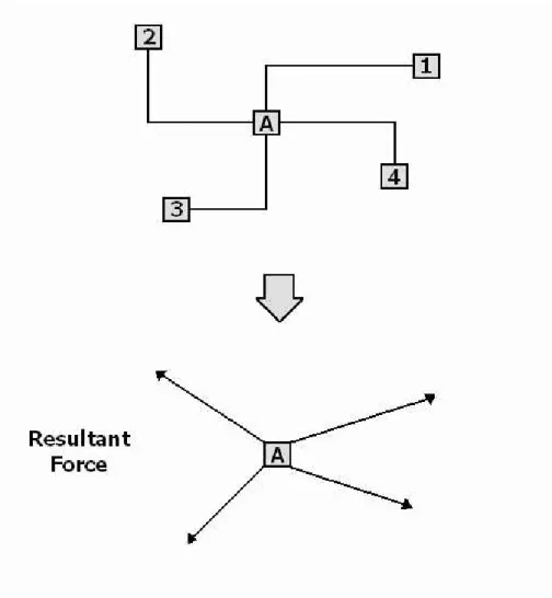
(16) clustered in one single I/O buffer block. • For a design with I/O buffers and a rectangular core layout region, we fix pad locations with an array of locations spaced uniformly within the core layout region. The detail will be described in Chapter 3.. Figure 2.2: The structure of I/O buffer block and signal pad [16].. 2.2. Force Directed Placement Flow. Once we model our I/O buffer blocks, we need to develop a placement flow to place I/O buffer blocks into the design. We adopt force directed placement to determine the location where we place I/O buffer blocks. Force directed placement was first proposed in the literature [18, 19]. This placement method applies an iterative placement procedure. The process starts with an initial placement and then selects a cell at a time to place the cell at it’s zero-force position which is computed numerically according to the connection with other cells. There is an example in Figure 2.3 for the force on a cell A connected with 6.
(17) four cells. The numerical analysis considers forces in x- and y-direction separately. In force directed placement, optimal solution corresponds to : • Force equilibrium :. P j. Cij · (Xj - Xi ) = 0 for all cell i. If the zero-force location is occupied by other cell, the placer will move the cell to another ideal location which is free to move in or move the cell which occupies the zero-force location to another ideal location. In particular, force directed placement improve placement by moving cells iteratively.. Figure 2.3: The force on a cell A connected with four cells. 7.
(18) 2.3. Area Array I/O Buffer Placement Methodology. In order to keep up the advantages in flip-chip design, current design flow and methodology are applied to satisfy system specification including many aspects such as placement [5], chip packaging [12, 13] and pad assignment[11]. We want to develop a methodology combined with I/O buffer modeling and buffer placement, and add this step to an existing design flow in Figure 2.4 [10] (similar to [14]) to present a more complete methodology in design cost and performance optimization.. 2.4. Problem Formulation. Performance of a digital system is measured by its cycle time. Shorter cycle time means higher performance. With considering the performance of a design at the layout level, signal propagation time and signal skew are two main factors. signal propagation time is defined as the path delay of the signal. Signal skew is defined as the difference of the delay between longest path and shortest path. In order to better the performance of the design, it is desirable to minimize the longest path delay and the signal skew. Our experiment focuses on I/O buffer placement in flip-chip design. We perform our placement in row-based design. We assume all signal bump can assign to any bump balls which are placed at pre-defined location. All the input/output signals are connected to cells through the I/O buffer blocks. The problem we concerned about is described as follows. Given an initial standard cell placement, a set of I/O buffers(which has corresponding set of signal bumps) IO = {io1 ,...,ion }, a set of signal bumps S = {s1 ,...,sn }, a user-specified skew range, a certain models for I/O buffer blocks, and a set of nets N = {n1 ,...,nm }, find a solution to simultaneously reduce the cell wirelength, the I/O wirelength and signal skew from signal bumps 8.
(19) Figure 2.4: Intrinsic area-array pad placement and routing flow from [10], and proposed modeling and placement step.. 9.
(20) to cells via buffer blocks. To achieve the goal, this problem requests to minimize the following objective functions Γ1 and Γ2 : Γ1 =. n X. dio j. j=1. +. m X. dj. (2.1). j=1. io Γ2 = | max dio j − min dj | 1≤j≤n. 1≤j≤n. (2.2). Γ1 gives the sum of wirelength of I/O nets and cell nets. dio j is the wirelength from signal bumps to cells via buffer blocks in the I/O net. dj is the wirelength between all cells in the net. The wirelength is determined by the Manhattan distance between two points.. W = |X1 − X2 | + |Y1 − Y2 |. (2.3). Γ2 gives the input/output signal skew by the absolute value between longest path and shortest path in I/O nets. dio j is the wirelength from signal bumps to cells via buffer blocks in the I/O net the same as Equation 2.1. In our experiment, we use the linear delay model same as wirelength to determine the path delay.. 10.
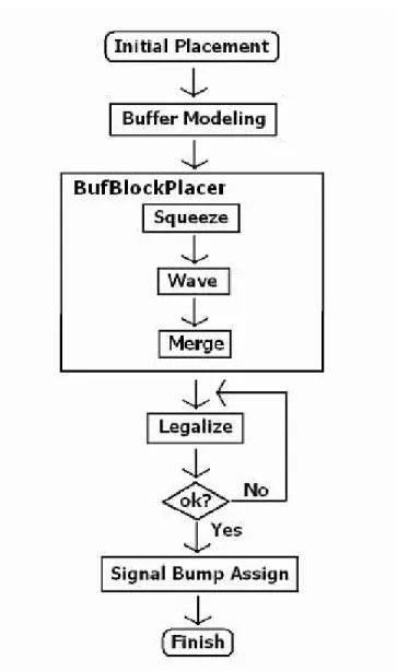
(21) Chapter 3 The I/O Buffer Block Placer Algorithm In this chapter, we present our I/O buffer block placer algorithm for I/O buffer placement and signal bump planning in flip-chip design. Our algorithm provides a new methodology which can be added to an existing non flip-chip design flow. We take a given initial standard cell placement, model the size of each I/O buffer block, place I/O buffer blocks into the design and assign signal bump to every I/O buffer block to achieve demands of flip-chip design. There are four stages of process in our I/O Buffer Block Placer Algorithm. In the process of buffer modeling, we model the size of each buffer according to the numbers of cells it connected. In the process of buffer block placer, we place those buffer blocks into the chip by squeezing the cells away from the position it occupied. In addition, we minimize longest path in the design and reduce the overhead of the wire length while adding those buffer blocks into the initial placement. During legalization, we move a set of costless cell from the longest row to the shortest row in order to maintain the rectangular shape of our placement. In signal bump assignment, we select a signal bump candidate which will not exceed a user-specific skew range for every I/O buffer to get a minimum skew design. The flow chart of our I/O buffer block placer algorithm is shown in Figure 3.1. 11.
(22) Figure 3.1: The flow chart of our buffer block placer algorithm. We will explain each part of our algorithm in the following sections.. 3.1. Buffer Modeling. In this stage, we build a lookup table for various type of buffer blocks based on the number of the cells it connected. As mentioned in Chapter 2, buffer blocks can share the clearance region for minimal spacing between ESD structures and active devices because of foundry rules. As a result, a buffer block with more single buffer grouped. 12.
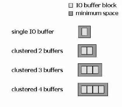
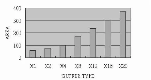
(23) together can reduce more area cost. In order to fit with the style of standard cell design and simplify the problem, we build our I/O buffer blocks with the same hight as the original row height of standard cell design, although real I/O buffer block may exceed the row height of standard cell design. The way we model our I/O buffer block is shown in Figure 3.2. For example, the I/O buffer block which clustered 4 buffers mean a signal buffer block which is able to drive 4 cells.. Figure 3.2: The model of our I/O buffer block. In the process of buffer modeling, we select the type of buffer block for every input/output based on the number of cells it connected. For example, an input pin connected with 8 cells will select a buffer block which is fit with the ability to drive 8 cells. In real design issue, the I/O buffer for output usually has bigger area than input because of the requirement for driven ability. In our buffer model, we simply treat those two kind of I/O buffer block as the same type. The size of each buffer block comes with two part. One is the minimal spacing between ESD structures and active devices. The other is the area of the buffer block itself with 13.
(24) ESD structure, latch-up ring, testing logic and driver circuit. The size of buffer block used in MCNC benchmark struct is shown in Figure 3.3.. Figure 3.3: The size of buffer block used in MCNC benchmark struct. 3.2. BufBlockPlacer. In execution of this buffer block placer, we first compute the geometry center of each net then we order the nets by the position of their geometry center from bottom to top then left to right. Second, we determine the size of the buffer block of each net by the table we made in buffer modeling. We place buffer blocks at the geometry center of every net to minimize the longest path from cells to the buffer block and also reduce the interconnection length on the side. We have three operations to place those I/O buffer blocks into the core : • Cell Squeeze : squeeze away the cell which occupied the location • Buffer Merge : merge two nearby buffer blocks into a single buffer block • Local Legalization : legalize the row length of the local rows. 14.
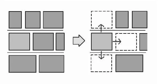
(25) We use Squeeze to squeeze the cell away from it’s location and place the buffer in that location until we get enough free space. We use Merge to merge two buffer blocks into one buffer block if they are physically neighbored. Merging two different buffer block together can reduce the total area by our look-up table. After some operations of Squeeze or Merge, the local rows may exceed the constraint of the length of row. We can use Wave to adjust them to maintain the rectangular shape of the chip.. 3.2.1. Cell Squeeze. Once we determine the location of the buffer block, we have to move out the cell which occupied the target location. We focus on the movement of the cell while it is been squeezing away. We define that our Squeeze operation has three directions to squeeze cells right, up and down. If we squeeze the cell right, all the cells on the right side of it including the cell itself will shift right. If we squeeze the cell up or down, the cell will move to the target row and take the same operation like squeeze right. The offset distance of shift right is the width of the cell which squeezes. The operation of the Squeeze is shown in Figure 3.4. We calculate the cost of Squeeze in all three directions by summing up the weight of every cell which have been moved. If the movement of the cell has changed the boundary box of the net it connected, the weight is recorded. The calculation of the weight is shown in Figure 3.5. Squeeze will choose the less cost direction to squeeze the cell. After the operation of Squeeze, the position of cell and free space will be updated to let BufBlockPlacer calculate the free space needed for the buffer block to be placed in. If the free space needed is less than the width of the cell we plan to squeeze, we will simply shift the cells right for the distance of free space needed instead of choosing which direction to squeeze. Once we get enough free space for the buffer block, we place the I/O buffer block into the free space. 15.
(26) Figure 3.4: The Squeeze has three direction to squeeze cells right, up and down. Figure 3.5: Moving the cell at the boundary of the net will change wire length of the net. 3.2.2. Local Legalization. After some operations of Squeeze, the length of the certain rows may exceed the constraint of the length of row. We develop a local legalization process which is 16.
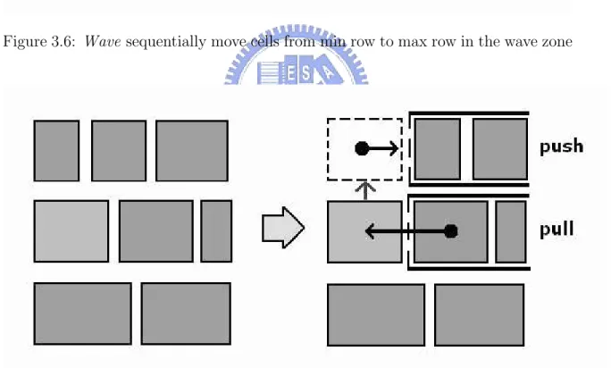
(27) inspired by the method used in Mongrel [20] to fix this problem. Once we squeeze some cells away from the positions they belong, we use Wave to move cells in the nearby area to reduce the impact on the change of length of the row caused by the operation of Squeeze. In our legalization procedure, we start with the initial placement (after Squeeze) and then sequentially move each less cost cell to it’s relaxed target location. The key point is that after each move we produce a feasible placement with free space for our buffer block. In the process of Wave, we set up a wave zone by the x-coordinate of the cell which has been squeezed in and the user-specified parameter W aveRange. If there is any buffer block in the wave zone, we redefine the range of the wave zone to avoid those buffer blocks. As shown in Figure 3.6, we sequentially move each less connectivity cell from the longest row to the shortest row. Every selected cell will move up/down to the cell in the next row and squeeze right the cells which are on the right side of it. The order we squeeze the cell is from bottom to top then left to right. As a result, the move in Wave will not affect the position of the buffer blocks which have been placed. The method we evaluate the weight of the cell which will be moved up or down are similar to the method we used in Figure 3.5. There are two sources of the weight while moving cell up/down. First, when we move out one cell from the row the cells on the right side of it should be pulled left. At the same time, when this cell move in the next row, the cells on the right side of it should be pushed right. The way we evaluate the weight of first part is shown in Figure 3.7. Second, the width of the cell which will be moved to the other row will affect the efficiency of legalization. Moving big cell out of the longest row means less legalization process will be needed. As a result, bigger cell will get lesser weight. We set up a parameter to adjust the ratio of weight between run time and wirelength reduction. We calculate the weight of every cell in the row then we can choose a less cost cell to move up/down. 17.
(28) Figure 3.6: Wave sequentially move cells from min row to max row in the wave zone. Figure 3.7: The weight in wave calculate the wire length cost in the operation pull and push. 3.2.3. Buffer Merge. In BufBlockPlacer, some operations like Squeeze and Merge may encounter that two buffers are physically neighbored. In order to reduce as much area as possible, we 18.
(29) use Merge to merge two buffer blocks into one. Due to the share of the clearance region of minimum spacing between ESD structures and active devices, the area of the merged single buffer block is less than the sum of two individual buffer blocks. We use look-up table to determine the size of the merged buffer block.. 3.2.4. The BufBlockPlacer Algorithm. In this section, we present a force-directed algorithm to place the buffer blocks into the location where the longest path from buffer block to the cells is minimized and the connection length is reduced as well. We place the buffer blocks in the order from bottom to top then left to right. As a result, every operation of cell squeeze, local legalization and buffer merge will not affect each other and the position of the placed buffer block will not be modified by the later move.The algorithm of the BufBlockPlacer is shown in Figure 3.8.. 3.3. Global Legalization. After performing BufBlockPlacer, the placement may still violate the constraint of the length of row. We use the same method as we mention in Section 3.2.2 to solve the problem. In stead of local wave zone in Wave, this procedure deal with the whole chip. We sequentially move each less cost cell to the next row from the longest row to the shortest row. This iterative process finish when there is no violations on the constraint of the length of row or the number of iteration exceeds an user-specified count.. 3.4. Signal Bump Assignment. Once we finish the placement of buffer blocks, we have to assign signal bumps to those buffer blocks. Since we adopt the flip-chip design, the location of the signal 19.
(30) Figure 3.8: The BufferPlacer algorithm. bump are uniformly over the chip. In the beginning of this process, we build up a set of locations in a gird for signal bumps to select. We apply two steps to determine the critical signal path. First, we handle the longest path from buffer block to the cell it connected in the design as a maximum delay path. Second, we select a closest signal bump location to that maximum delay path to minimize the delay of the maximum delay path. Here we get a maximum signal delay called MaxDelay for all other input/output nets.. 1 2. We set a parameter called USSR (user-specified skew. 1 Note that the input/output net in our signal bump assign is a net with input/output signal, the buffer block and the cell it connected. 2 And the skew is the difference in wirelength between input/output net and the longest input/output net.. 20.
(31) range) to control the skew for all input/output net. After we finish the signal bump assignment for the net with longest path, we continue the next assignment for the net with the longest path to the rest of nets until all nets are assigned. For instance, there are five cells in in Figure 3.9 cell 1, cell 2, cell 3, cell 4 and cell5. Cell 1, cell 2 and cell 3 are in the same net, so they all connect to the same buffer block. Cell 4 and cell 5 are in another net, so they connect to another buffer block. Cell 1 to it’s buffer block is the longest path in this example, so we set it as MaxDelay. We assign a signal bump A for it. Cell 5 is the longest path in another net, so we assign sign bump B to it without exceed USSR compared with MaxDelay.. Figure 3.9: An example for signal bump assignment. 3.5. Summary of Our Algorithm. In this chapter, we propose an I/O buffer placement method with four-stage approach. In the stage of buffer modeling, we model the size of each buffer according 21.
(32) to the number of cells it connected. In buffer block placement, we place those buffer blocks into the chip by squeezing the the cells away from the location it occupied. During global legalization, we move a set of less cost cell from the longest row to the shortest row in order to maintain the rectangular shape of our placement. In order to consider skew constraint, we select a signal bump candidate which may not exceed an user-specific skew range. We use an example to show how our algorithm work. The placement results are shown in Figure 3.10, 3.11, 3.12 and 3.13, respectively.. Figure 3.10: The initial placement, those rectangles represent cells.. 22.
(33) Figure 3.11: The placement placed with buffer blocks after the execution of BufBlockPlacer, dark rectangles represent buffer blocks and those lines represent the connection of the cells.. Figure 3.12: A fine tuned placement after the process of Local legalization. 23.
(34) Figure 3.13: The final placement after the process of Signal Bump Assignment, those squares over the cells represent signal bumps.. 24.
(35) Chapter 4 Experimental Results We implemented the I/O buffer placer algorithm in C++ programming language. The platform is Intel Pentium 4 2.4GHz CPU with 1.5GB memory. The initial placements based on some MCNC benchmarks(in Table 4.1) are obtained from the placer FENG SHUI [21], with aspect ratio 1.0. The number of signal bumps of the flip-chip design are scaled from IBM SA-27E area-array copper technology[5]. The I/O buffer block model of flip-chip design has been described in Chapter 2 and Chapter 3. We compare our results with the peripheral design for area and wirelength. The pad size of the peripheral design is 100 × 100um and the pad pitch is 100um[22]. The minimum space between I/O pads and the core in peripheral design is set the same as the row height of the standard cell. Table 4.2 shows the experimental results in area on MCNC benchmarks summarized in Table 4.1. The width of the area in flip-chip design is equal to the length of longest row. Since industry2 is a big design Table 4.1: Number of cells, nets and placement benchmarks. Benchmark struct biomed industry2. I/O terminals in some MCNC standard cell Cells 1952 6514 12637. 25. Nets I/Os 64 1920 97 7052 13419 495.
(36) Table 4.2: Area comparisons between our approach and the peripheral design with the MCNC benchmark. Peripheral design BufBlockPlacer Improvement Initial # Circuit. of. area. Area. Area. in area. cells. (um2 ). (um2 ). (um2 ). (%). 16.91 10.13 35.73. struct. 1952. 11.47E+6. 15.91E+6. 13.22E+6. biomed. 6514. 52.48E+6. 61.57E+6. 55.33E+6. industry2. 12639. 10.45E+7. 16.96E+7. 10.90E+7. Table 4.3: Wirelength comparisons between our approach and the peripheral design with the MCNC benchmark and the result of signal skew. Improvement BufBlockPlacer Peripheral design # # Circuit struct. of. of. Wirelength. Wirelength. Skew. in wirelength. nets. signals. (um). (um). (um). (%). 1920. 64. 656856. 613726. 5250. 6.57 12.94 35.92. biomed. 7052. 97. 2.992E+6. 2.605E+6. 13094. industry2. 13419. 495. 1.416E+7. 9.074E+6. 19564. with more than 400 I/Os, the size of initial peripheral design is not compatible with such amount of I/Os, we increase the space between I/O pads and the core for industry2 in peripheral design to fit the amount of the I/O pad. Table 4.3 shows the experimental result in wirelength and skew on MCNC benchmarks summarized in Table 4.1. The estimation of wirelength and skew has been described in Chapter 2. We obtain better I/O timing performance by smaller I/O wirelength. The wirelength from I/O nets to pads in peripheral design are estimated by the average distance from the net to the boundary of I/O pads. Table 4.4 shows the experimental result in run time on MCNC benchmark industry2. The run time of our placer mainly comes from the legalization process. We adjust the parameter of the weight between wirelength and run time in the legalization process to see how it affects the run time and the performance of our placer. The final result for these circuits for both peripheral and flip-chip design are 26.
(37) Table 4.4: Run time comparisons for our I/O buffer placer with the MCNC benchmark industry2, we adjust the parameter of the weight to make legalization process consider wirelength only or both wirelength and run time. Wirelength Run time Area industry2 with 2 (sec) (um) (um ) legalization consideration 2156 11.08E+7 8.942E+6 Wirelength only 427 Wirelength and run time 10.90E+7 9.074E+6. shown from Figure 4.1 to 4.4. From the result shown in Table 4.2 and Table 4.3, we can see that a significant improvement in chip size and wirelength can be achieved by using our I/O buffer placer methodology. Table 4.4 shows that we can trade a few cost in wirelength for a decent improvement in run time.. 27.
(38) Figure 4.1: The placement of struct with peripheral design (from the placer FENG SHUI [21]).. Figure 4.2: The final result of struct with BufBlockPlacer.. 28.
(39) Figure 4.3: The placement of biomed with peripheral design.. Figure 4.4: The final result of biomed with BufBlockPlacer.. 29.
(40) Figure 4.5: The placement of industry2 with peripheral design.. Figure 4.6: The final result of industry2 with BufBlockPlacer.. 30.
(41) Chapter 5 Conclusion and Future Works In this thesis, we have present our I/O buffer placer algorithm in design cost and performance optimization for high-end flip-chip design. Our methodology combined with I/O buffer modeling and buffer placement. We can add this step to an existing design flow to convert the initial design to flip-chip design. Experimental results have shown that our algorithm has better performance compared with peripheral design in high I/O count circuits. For future improvement of our placement method, developing a complete placement flow with I/O buffer floorplanning for flip-chip design will be a better way to optimize the performance of placement in flip-chip design and add some more constraints into our placement algorithm like power supply noise or voltage drop threshold violation cause by IR drop. We also need to develop a better algorithm to further reduce the signal skew.. 31.
(42) Bibliography [1] A. Chandrakasan, W.J. Bowhill, and F. Fox, “Design of High-Performance Microprocessor Circuits,” IEEE Press,, 2001. [2] P. Dehkordi and D. Bouldin, “Design for Packageability: The Impact of Bonding Technology on the Size and Layout of VLSI Dies,” Proc. of Multi-Chip Module Conference, pp. 153-159 , 1993. [3] V. Maheshwari, J. Darnauer, J. Ramirez, and W.W.-M. Dai, “Design of FPGAs with Area I/O for Field Programmable MCM,” In Proceedings ACM Symposium on Field Programmable Gate Arrays, pp. 17-23, 1995. [4] P.A. Sandborn, M.S. Abadir, and C.F. Murphy, “The Tradeoff Between Peripheral and Area Array Bonding of Components in Multichip Modules,” IEEE Transactions on Components, Packaging, and Manufacturing Technology - Part A, pp. 249-256, 1994. [5] P.H. Buffet, J. Natonio, R.A. Proctor, Y.H. Sun, and G. Yasar, “Methodology for I/O cell Placement and Checking in ASIC Designs Using Area-Array Power Grid,” In IEEE Custom Integrated Circuits Conference, pp. 125-128, 2000. [6] G. Yasar, C. Chiu, R.A. Proctor, and J.P. Libous, “I/O Cell Placement and Electrical Checking Methodology for ASICs with Peripheral I/Os,” In IEEE International Symposium on Quality Electronic Design, pp. 71-75, 2001.. 32.
(43) [7] R. Farbarik, X. Liu, M. Rossman, P. Parakh, T. Basso, and R. Brown, “CAD Tools for Area-Distributed I/O Pad Packaging,” In IEEE Multi-Chip Module Conference, pp. 125-129, 1997. [8] P.S. Zuchowski, J.H. Panner, D.W. Stout, J.M. Adams, F. Chan, P.E. Dunn, A.D. Huber, and J.J. Oler, “I/O Impedance Matching Algorithm for HighPerformance ASICs,” In IEEE International ASIC Conference and Exhibit, pp. 270-273, 1997. [9] R.J. Lomax, R.B. Brown, M. Nanua, and T.D. Strong, “Area I/O Flip-Chip Packaging to Minimize Interconnect Length,” In IEEE Multi-Chip Module Conference, pp. 2-7, 1997. [10] C. Tan, D. Bouldin, and P. Dehkordi, “Design Implementation of Intrinsic Area Array ICs,” In Proceedings 17th Conference on Advanced Research in VLSI, pp. 82-93, 1997. [11] Joel Mcgrath, “Chip/Package Co-Design: The bridge between chips and systems,” In Advanced Packaging, June 2001. [12] J.C.. Parker,. R.J.. Sergi,. D.. Hawk,. and. M.. Diberardino,. “IC-. Package Co-Design Supports Flip-Chips,” EE Times, November 2003. http://www.eedesign.com/story/OEG20031113S0055. [13] K.-Y. Chao and D.F. Wong, “Signal Integrity Optimization on the Pad Assignment for High-Speed VLSI Design,” In Proceedings IEEE International Conference on Computer-Aided Design, pp. 720-725, 1995. [14] H.-M. Chen, I.-M Liu, D.F. Wong, M. Shao, L.-D. Huang, “I/O Clustering in Design Cost and Performance Optimization for Flip-Chip Design,” In Proceedings the IEEE International Conference on Computer Design, pp. 562-567, 2004 33.
(44) [15] J.N. Kozhaya, S.R. Nassif, and F.N. Najm, “I/O Buffer Placement Methodology for ASICs,” In IEEE International Conference on Electronics, Circuits and Systems, pp. 245-248, 2001. [16] T. Schaffer, A. Glaser, and P.D. Franzon, “Chip-Package Co-Implementation of a Triple DES Processor,” IEEE Transactions on Advanced Packing, pp. 194202, 2004. [17] A.E. Caldwell, A.B. Kahng, S. Mantik, and I.L. Markov, “Implications of AreaArray I/O for Row-Based Placement Methodology,” In IEEE Symposium on IC/Package Design Integration, pp. 93-98, 1998. [18] M. Hanan and J.M. Kurtzberg, “Placement Techniques,” In M.A. Breuer, Editor, Design Automation of Digital Systems, Prentice -Hall Inc, Englewood Cliffs, New Jeresey, pp. 213-282, 1972. [19] Quinn, Jr and Breuer, “A Force Directed Component Placement Procedure for Printed Circuit Boards,” IEEE Transactions on Circuits and Systems, June 1979. [20] S.-W. Hur and J. Lillis, “Mongrel: hybrid techniques for standard cell placement,” In Proceedings IEEE International Conference on Computer-Aided Design, pp. 165-170, 2000. [21] P.H. Madden, “Reporting of Standard Cell Placement Results,” IEEE Transactions on Computer-Aided Design of Integrated Circuits and Systems, 21(2):240247, February 2002. [22] C. Tan, D. Bouldin and P. Dehkordi, “An intrinsic area-array pad router for ICs,” In Proceedings of Tenth Annual IEEE International ASIC Conference, pp. 265-269, Sept. 1997.. 34.
(45) 作者簡歷 張加易,民國六十七年二月出生於嘉義縣。大學畢業於國立中正大學 電機工程學系。民國九十二年九月進入國立交通大學電子研究所就 讀,從事 VLSI 實體設計自動化方面相關研究。民國九十四年六月取 得碩士學位。.
(46)
數據
![Figure 2.1: Annotated photomicrograph of DES IC with I/O buffer blocks grouped at the center of the chip [16].](https://thumb-ap.123doks.com/thumbv2/9libinfo/8118557.165806/15.918.267.635.229.753/figure-annotated-photomicrograph-des-buffer-blocks-grouped-center.webp)
![Figure 2.2: The structure of I/O buffer block and signal pad [16].](https://thumb-ap.123doks.com/thumbv2/9libinfo/8118557.165806/16.918.213.678.377.675/figure-structure-i-o-buffer-block-signal-pad.webp)
+7
![Figure 2.4: Intrinsic area-array pad placement and routing flow from [10], and pro- pro-posed modeling and placement step.](https://thumb-ap.123doks.com/thumbv2/9libinfo/8118557.165806/19.918.154.745.310.898/figure-intrinsic-array-placement-routing-posed-modeling-placement.webp)
Outline
相關文件
The buffer cell sees very different optical influence from different neighboring cells. Center features almost remain
If the best number of degrees of freedom for pure error can be specified, we might use some standard optimality criterion to obtain an optimal design for the given model, and
Let us suppose that the source information is in the form of strings of length k, over the input alphabet I of size r and that the r-ary block code C consist of codewords of
微算機基本原理與應用 第15章
To complete the “plumbing” of associating our vertex data with variables in our shader programs, you need to tell WebGL where in our buffer object to find the vertex data, and
LTP (I - III) Latent Topic Probability (mean, variance, standard deviation).. O
This algorithm has been incorporated into the FASTA program package, where it has decreased the amount of memory required to calculate local alignments from O(NW ) to O(N )
; actual input count buffer BYTE count DUP(?) ; holds input chars KEYBOARD ENDS. • Requires a predefined structure to be set up that describes the maximum input size and holds the
