物理研究所
博 士
論
文
垂直式高分子金屬基極電晶體
Vertical Polymer Metal-base Transistor
研 究 生:趙宇強
指導教授:孟心飛 教授
垂直式高分子金屬基極電晶體
Vertical Polymer Metal-base Transistor
研 究 生:趙宇強 Student:Yu-Chiang Chao
指導教授:孟心飛 Advisor:Hsin-Fei Meng
國 立 交 通 大 學
物 理 研 究 所
博 士 論 文
A DissertationSubmitted to Institute of Physics College of Science National Chiao Tung University in partial Fulfillment of the Requirements
for the Degree of Doctor of Philosophy
in Physics July 2008
Hsinchu, Taiwan, Republic of China
viii
國立交通大學物理研究所博士班
摘
要
本論文旨在實現新穎有機電子元件並且探討其特性。本論文展示了高分子熱載子電晶體與 高分子空間電荷限制電晶體這兩種垂直式高分子金屬基極電晶體,以及一種發光高分子空間電 荷限制電晶體。首先將討論具有不同射極材料的高分子熱載子電晶體。當熱載子電晶體使用具 有高能隙之高分子為射極材料時,共射電流增益為 25。當元件使用具有低能隙之高分子為射 極材料時,共射電流增益為 31 且輸出電流密度為 31 mA/cm2。當元件的射極材料是混合有低 能隙與高能隙的高分子時,電流密度可以達到 428 mA/cm2。使用此電晶體去驅動高分子發光 二極體時,可以達到 3000 cd/m2的亮度。接著將討論高分子空間電荷限制電晶體的操作原理與 特性。柵極上的孔洞大小與孔洞密度可以控制空間電荷限制電晶體的操作特性。在高真空下退 火與增加絕緣層於柵極旁更可提升高分子空間電荷限制電晶體的特性。目前高分子空間電荷限 制電晶體的最大輸出電流密度是 27 mA/cm2,開關比為 428,電流增益約為 104。最後將討論 由上發光高分子發光二極體垂直堆疊於高分子空間電荷限制電晶體所製成之發光高分子空間 電荷限制電晶體。當柵極電壓調變於-0.9 伏到 0.9 伏時,發光強度將可以被調變並且最亮可達 1208 cd/m2。此發光高分子空間電荷限制電晶體的電流效率為 10 cd/A。由於向上發出的光將 不會被在下方的高分子金屬基極電晶體所阻擋,當電晶體與發光二極體面積相同時,基本上可 以達到 100 %的開口率。
ix
Vertical Polymer Metal-base Transistor
student:Yu-Chiang Chao
Advisors:Dr. Hsin-Fei Meng
Institute of Physcis
National Chiao Tung University
ABSTRACT
This dissertation aims to realize and characterize novel organic electronic devices. Two vertical polymer metal-base transistors, namely polymer hot-carrier transistor and polymer space-charge-limited transistor, and one light-emitting polymer space-charge-limited transistor are demonstrated. First, polymer hot-carrier transistors with various emitter materials are discussed. For the metal-base hot-carrier transistor with high bandgap emitter, common-emitter current gain of 25 is obtained. For the metal-base hot-carrier transistor with low bandgap emitter, common-emitter current gain of 31 and the current density as high as 31 mA/cm2 are obtained. Furthermore, for the device using blend of high and low bandgap polymer as the emitter, the current density 428 mA/cm2 is achieved. The brightness of 3000 cd/m2 is obtained as a polymer light-emitting diode is driven by the hot-carrier transistor. Second, operation principles and electrical properties of the polymer space-charge-limited transistor are studied. The characteristics of the transistor can be tuned by the diameters and the density of the openings on the grid. Annealing in high vacuum as well as adding insulator on grid metal can further enhance the performance of the polymer space-charge-limited transistor. So far, output current density is about 27 mA/cm2, on/off ratio is 428, and current gain is around 104. Finally, a light-emitting polymer space-charge-limited transistor is realized by vertically stacking a top-emitting polymer light-emitting diode on a polymer space-charge-limited transistor. As the grid base voltage varies from −0.9 V to 0.9 V, the light emission is turned on and off with on luminance up to 1208 cd/m2. The current efficiency of the light-emitting transistor is 10 cd/A. The aperture ratio is basically 100 % because the light emitted upward is not shielded by the vertical metal-base transistor underneath with roughly the same area.
x
throughout this research work. I am grateful for his commitment in providing his students effective environment and broad experience. He was always willing to encourage me to conquer obstacles. Numerous critical discussions are also appreciated.
Professor Sheng-Fu Horng, Professor Chain-Shu Hsu, Professor Yu-Tai Tao, Professor Ray-Nien Kwo, Professor Hsiao-Wen Zan, and Professor Heh-Nan Lin are appreciated for their
suggestions and comments on this thesis.
I would like to express my gratitude to all current and former PhD and Master students who cooperated with me throughout my past four years. Especially for those who have had a positive influence on my work.
Finally, I especially thank my family members for their unconditional support and patience. I feel a deep sense of gratitude for my parents. They have always been supportive to me at their best in my life. I now realize how much I still have to learn from their admirable tenacity.
Thank you all. ~~
Yu-Chiang Chao July 9, 2008
xi
Contents
Abstract viii Acknowledgements x Contents xi List of Figures xv 1 Introduction 1 1.1 Organic materials………. 2 1.1.1 Polymers……….. 21.1.2 Small molecular weight materials……… 5
1.2 Fundamental organic electronics……….. 8
1.2.1 Organic light-emitting diodes………... 8
1.2.2 Organic photovoltaics………... 11
1.2.3 Organic field-effect transistors………. 14
1.3 Motivation……… 17
1.4 Overview of the thesis………. 19
2 Theoretical background 21 2.1 Semiconducting polymer………. 21
2.1.1 Molecular orbital and bonding………. 21
2.1.2 Electronic excitations………... 25
2.2 Metal/organic interface………. 28
2.2.1 Energy band diagram……… 28
2.2.2 Image-force lowering………... 30
2.3 Carrier injection and transport……….. 32
xii
2.5.2 Bipolar junction transistors……….. 43
2.5.3 Metal-base transistors………... 45
2.5.4 Permeable-base transistors………... 46
2.5.5 Static-induction transistors………... 48
2.5.6 Vacuum tube triodes………. 51
3 Polymer hot-carrier transistor 53 3.1 Introduction……….. 53
3.1.1 Background……….………. 53
3.1.2 Organization of this chapter………. 55
3.2 Polymer hot-carrier transistor with high bandgap emitter…………... 55
3.2.1 Motivation……… 55
3.2.2 Device structure and fabrication……….. 56
3.2.3 Electrical characteristics………... 59
3.2.4 Summary of section 3.2……… 61
3.3 Polymer hot-carrier transistor with low bandgap emitter………. 61
3.3.1 Motivation……… 61
3.3.2 Device structure and fabrication……….. 63
3.3.3 The effect of the insulating layer thickness……….. 65
3.3.4 The effect of the emitter-base diode current density………… 67
3.3.5 Electrical characteristics………... 68
3.3.6 Frequency response……….. 69
3.3.7 Summary of section 3.3……… 70
3.4 Polymer hot-carrier transistor with a blend of low and high bandgap materials as emitter………... 71
xiii
3.4.3 Electrical characteristics………... 72
3.4.4 Connection between the polymer hot-carrier transistor and a polymer light-emitting diode………... 72
3.4.5 Summary of section 3.4……… 74
3.5 Summary of chapter 3……….. 74
4 Polymer space-charge-limited transistor 76 4.1 Introduction……….. 76
4.1.1 Background……….………. 76
4.1.2 Organization of this chapter………. 78
4.2 Polymer space-charge-limited transistor with low current density….. 78
4.2.1 Motivation……… 78
4.2.2 Device structure and fabrication……….. 79
4.2.3 Spin-coated polystyrene spheres as shadow mask…………... 82
4.2.4 Device characteristics………... 83
4.2.5 The effect of the opening diameter and density………... 85
4.2.6 Summary of section 4.2……… 86
4.3 Polymer space-charge-limited transistor with high current density…. 87 4.3.1 Motivation……… 87
4.3.2 Device structure and fabrication……….. 87
4.3.3 High density polystyrene spheres as shadow mask………….. 89
4.3.4 Electrical characteristics………... 90
4.3.5 Operation mechanism………... 94
4.3.6 Summary of section 4.3……… 97
4.4 Summary of chapter 4……….. 97
5 Light-emitting polymer space-charge-limited transistor 99 5.1 Introduction and motivation...……….. 99
5.2 Device structure and fabrication……….. 101
5.3 Electrical and optical characteristics……… 104
5.3.1 High performance polymer space-charge-limited transistor… 104 5.3.2 Light-emitting polymer space-charge-limited transistor…….. 106
xv
List of Figures
1.1 Molecular structure of widely used conjugated polymers………. 4
1.2 Molecular structure of widely used small molecular weight materials….. 7
1.3 Structure of a single-layer polymer electroluminescent diode…………... 10
1.4 Schematic energy level diagram for an ITO/PPV/Al LED……… 10
1.5 Evolution of organic light-emitting diode structures………. 10
1.6 Four device architectures of conjugated polymer-based photovoltaic cells………. 12
1.7 Schematic of the bottom-gate organic field-effect transistors with various structures……… 15
1.8 Crystallite structure in polythiophenes………... 16
2.1 Structures of trans- and cis-polyacetylene……….. 22
2.2 sp2-hybridized atom……… 23
2.3 Formation of σ bond and π bond……… 23
2.4 The energy levels of a π-conjugated molecule………... 24
2.5 Period doubling in dimerized chain………... 25
2.6 Schematic form of a neutral soliton on a trans-polyacetylene chain…….. 26
2.7 Electronic structure leading to various charge and spin state of a soliton. 26 2.8 Schematic energy band diagrams for polarons and bipolarons………….. 27
2.9 Energy band diagram of a metal-semiconductor contact………... 29
2.10 Energy band diagrams of rectifying metal / n-type semiconductor contact……… 29
2.11 The energy band diagram for the interface between a metal surface and a vacuum……… 31
2.12 Basic steps of electroluminescence……… 40
2.13 A schematic representation of the elementary processes………... 41
2.14 A p-n-p bipolar transistor………... 44
xvi
3.1 The structures and energy band diagram of polymer hot-carrier
transistor with high bandgap emitter……….. 57 3.2 The I-V curves of emitter-base and base-collector diodes………. 60 3.3 The characteristics of the polymer hot-carrier metal-base transistor in
common-emitter configuration………... 60 3.4 The characteristics of the polymer hot-carrier metal-base transistor in
common-emitter configuration………... 61 3.5 The structures and energy band diagram of polymer hot-carrier
transistor with low bandgap emitter………... 64 3.6 The current gain β as a function of LiF thickness of the hot-carrier
transistor………. 66 3.7 The AFM image of Al base on P3HT………. 66 3.8 The current gain β as a function of EB diode current density at 4 V……. 68 3.9 The base voltage of various devices with different emitter thickness…… 68 3.10 The characteristics of the polymer hot-carrier transistor in common
emitter configuration……….. 69 3.11 Frequency response of the hot-carrier transistor……… 70 3.12 The characteristics of the polymer hot-carrier transistor in common
emitter configuration……….. 73 3.13 Connection between hot-carrier transistor and polymer light-emitting
diode………... 73 3.14 The luminance of the polymer light-emitting diode driven by the
polymer hot-carrier transistor………. 74 4.1 Device structure and energy band diagram of the polymer
space-charge-limited transistor………... 80 4.2 The potential profile of the transistor………. 81 4.3 The AFM images of the Al grid………. 83 4.4 Collector current I and grid current C I as a function of collector G
xvii
4.5 ( )12 C
I
− against −VC when V = 0.5 V………. G 85
4.6 The characteristics of the polymer space-charge-limited transistor……... 86 4.7 Device structure and energy band diagram of polymer
space-charge-limited transistor with an Al grid with random submicron
openings……….. 88 4.8 Al grid with various opening diameter………... 91 4.9 The electric characteristics of the polymer space-charge-limited
transistor with various grid voltages applied……….. 93 4.10 The device structure near one opening and operation principle of
polymer space-charge-limited transistor……… 96 5.1 Device structure of the polymer space-charge-limited transistor………... 102 5.2 Device structure of the top-emitting polymer light-emitting transistor…. 103 5.3 Energy profile of the top-emitting polymer light-emitting transistor……. 103 5.4 The electric characteristics of the polymer space-charge-limited
transistor with 2000 Å openings on Al grid………... 105 5.5 The efficiency and luminance of the top-emitting polymer light-emitting
diode………... 107 5.6 The electric characteristics of the polymer light-emitting transistor with
1
Introduction
The goal of this introductory chapter is to provide the reader with a concise introduction of organic materials and devices. Material properties and optoelectronic properties of organic electronic materials, including small molecular weight materials and polymer, are introduced and discussed. Benefits and drawbacks of current state-of-the-art in organic devices and processing technology are also surveyed. Its intention is not to provide a complete description of organic materials and devices, but rather, it aims to provide springboards for further reading through the references that are cited.
In Section 1.1, many organic electronic materials and organic semiconductors will be introduced. Development history of the organic materials is also provided in this section.
In Section 1.2, the current state-of-the-art in organic electronics is summarized and the remaining challenges are outlined. Discussion in this section is focus on organic light-emitting diodes, organic photovoltaics, and organic field-effect transistors. The techniques utilized for fabricating organic electronics and photonic devices are briefly introduced. In addition to commonly used preparation methods, some aspects that make organic electronics unique are also included in this section.
summary of the challenges and motivations of this research work is present.
Finally, in Section 1.4, we overview the topics present in this thesis for various reader's interests.
1.1 Organic materials
Every living organism is made of organic chemicals. The food you eat; the medicines you take; and the wood, paper, plastics, and fibers that make modern life possible are all organic chemicals. However, only those molecules have pronounced optical and electrical qualities can be utilized for electronics. In general, the organic electronic materials that find use in organic electronics are more complex than simple organic materials, but less complex than most biological materials. The class of organic electronic materials can be subdivided into two clearly distinct categories: small molecular weight organic materials and polymers.
1.1.1 Polymers
The conventional polymer is largely used due to their plastic deformability, mechanical strength, low weight, and usually high resistivity. These characteristics allowed plastic materials enter every sector of our civilization, from low cost simple utilities to highly sophisticated technologies such as aircraft construction. Ever since the polymer became important in technology, their usefulness can be significantly enhanced if their conductivity could be raised. Metal could then be replaced by light and easily processible materials.
At the beginning of the 1970s, the Japanese chemist Shirakawa found that it was possible to synthetisize polyacetylene (CH)n in a new way. Shirakawa synthesized
trans-polyacetylene by accidentally adding “a thousand-fold too much catalyst” to the reaction vessel. To Shirakawa's surprise, this time a beautiful silvery film appeared.
inorganic polymer sulphur nitride, (SN)x. When MacDiarmid heard about Shirakawa's
discovery at a seminar in Tokyo, he invited Shirakawa to the University of Pennsylvania in Philadelphia. After Shirakawa and MacDiarmid modified polyacetylene by oxidation with iodine vapor, they knew that the optical properties changed in the oxidation process and asked Heeger to have a look at the films. After measured the conductivity of the iodine-doped trans-polyacetylene, the incredible increase of ten million times the original conductivity was discovered. In the summer of 1977, Alan Heeger, Alan MacDiarmid and Hideki Shirakawa, and co-workers, published their discovery in the article "Synthesis of electrically conducting organic polymers: Halogen derivatives of polyacetylene (CH)n" in The Journal of Chemical
Society, Chemical Communications.[1] The discovery was considered a major breakthrough, and Alan Heeger, Alan MacDiarmid and Hideki Shirakawa have been awarded the Nobel Prize in Chemistry in the year 2000 for showing how plastic can be made to conduct electric current.[2] Since then the field has grown immensely, and also given rise to many new and exciting applications.
The properties of a polymer are strongly related to the physical arrangement of monomers along the backbone of the chain. Polymers which contain only one type of monomer are known as homopolymers, while polymers containing a mixture of monomers are known as copolymers.
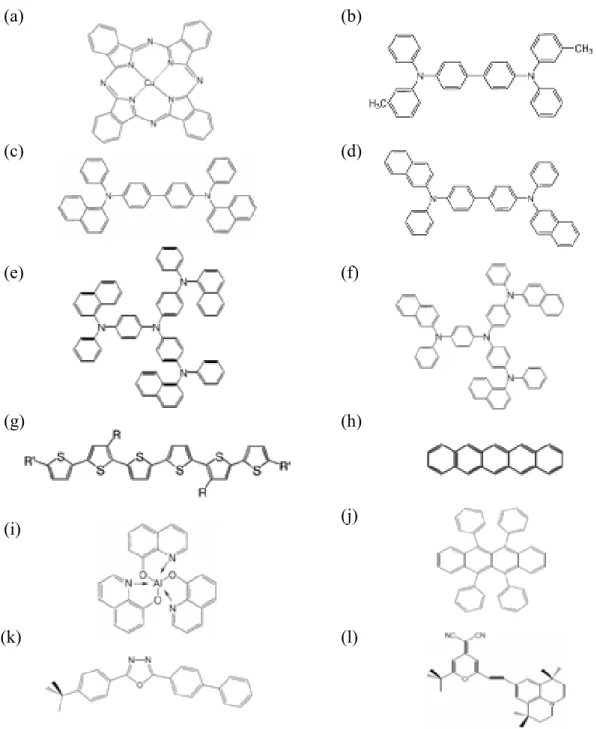
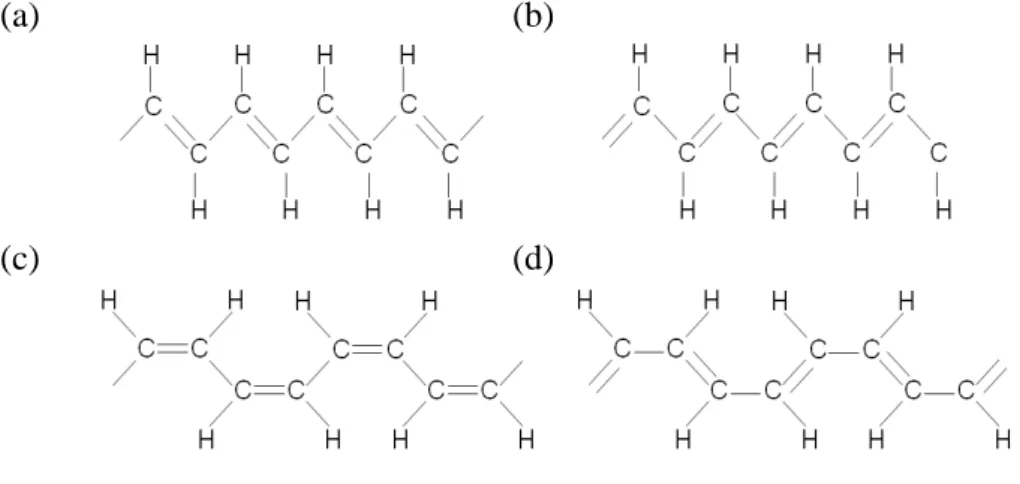
The conducting conjugated polymer consists of a long chain of carbon atoms with alternating single and double bonds between them, each with one hydrogen atom. The structure of polyacetylene is shown in Fig. 1.1(a) as a typical example.
Figure 1.1 Molecular structure of widely used conjugated polymers: (a) polyacetylene; (b) poly(3,4-ethylenedioxythiophene) : poly(styrenesulfonate) (PEDOT:PSS); (c) poly(9,9-dioctylfluorene-co-N-(4-butylphenyl)diphenylamine) (TFB); (d) poly(9,9-dioctylfluorene-co-bis-N,N-(4-butylphenyl)-bis-N,N-phenyl-1,4-phenylenediam
ine) (PFB); (e) poly[N,N'-bis(4-butylphenyl)-N,N'-bis(phenyl)-benzidine] (polyTPD); (f) poly(p-phenylenevinylenes) (PPV); (g) poly[9,9-dioctylfl uorenyl-2,7-diyl] (PFO); (h) poly-[2-methoxy,(5-2'-ethyl-hexyloxy)-p-phenylenevinylene] (MEH-PPV); (i) poly(9,9-dioctylfluorene-co-benzothiadiazole) (F8BT); (j) poly[3-hexylthiophene] (P3HT); (k) poly[5,5'-bis(3-alkyl-2-thienyl)-2,2'-bithiophene) (PQT); (l) poly[(9,9-dioctylfluorene-co-bithiophene] (F8T2); (m) poly(9-vinylcarbazole) (PVK). (a) (b) (c) (d) (e) (f) (g) (h) (i) (j) (k) (l) (m)
and organic solar cells. As shown in Fig. 1.1(b), PEDOT:PSS is a water-soluble transparent conducting polymer, which enabled the fabrication of all plastic polymer light-emitting diodes (PLEDs). PEDOT:PSS can be used as a transparent anode. Currently, it serves as the hole transport layer to develop PLEDs for commercial products.
Structures of PPV and PPV derivatives (MEH-PPV) are shown in Fig. 1.1(f) and 1.1(h). The most commonly used PPV is typically deposited by spin coating a precursor polymer, and then thermal treatment is used to convert the precursor to PPV. PPV also used as hosts for low gap emitter.[3] PFO is also the material used in the blue PLEDs as shown in Fig. 1.1(g). Following the first blue PFO-based PLED was developed in 1991 [4], efforts was conducted on developing commercially viable devices based on these polymer.
Polythiophenes and P3HT-based PLEDs and FETs are widely studied.[5,6] Due to it relatively low gap, the polythiophenes are red emitters. However, the relatively poor lifetime of polythiophene-based PLEDs inhibits their commercialization. On the other hand, P3HT is a commonly used material in FETs. Under proper treatment, the mobility can be increased and the performance of the FETs can be optimized.
1.1.2 Small molecular weight materials
The phenomenon of organic electroluminescence was first discovered by Pope in 1963.[7] But, the development of organic light-emitting diode actually began in the late 1970s by Tang and coworkers. Their research led eventually to the discovery of
the first efficient multi-layered organic electroluminescent device.[8] Since then, tremendous progress has been made in the field of organic electroluminescence. Among all efforts to improve the performance of organic light-emitting diode, the continuing discovery of new and improved electroluminescent materials is the most essential one.
Small molecular weight materials consist of molecules with several to a few hundred atoms. Small molecular weight materials were the initial focus of physicists and engineers who seeking to understand the optoelectronics properties of organic materials. Structure of some small molecular weight materials are shown in Fig. 1.2. Fig. 1.2(a) shows the structure of CuPC which is widely used as an hole transport layer. However, depending on the other layer, it may inhibit hole injection [9] or enhance it [10]. TPD is another material commonly used as hole transport layer as shown in Fig. 1.2(b). But, its relatively low glass transition temperature around 65℃ causes a failure of OLED as TPD recrystallized. The recrystallization may be suppressed by adding guest molecule such as rubrene. However, it may result in red electroluminescence from rubrene. Hence, NPB is developed with a structure similar to TPD but the methylphenyl groups are replaced by naphthylphenyls. The modification significantly enhance the stability of the OLED due to the increased glass transition temperature around 95℃.
Alq3 is the most widely used electron-transport and host emitting material in OLEDs. It is still one of the most robust electron-transport backing layers in OLED, particularly with the help of the hole blocking layer to trap the hole carriers from injecting into Alq3.[11] It is mot only commonly used as a green emitter, but also as a host for lower-gap emitter guest molecules. It has been found by the time-of-flight technique that the drift mobility of electrons in Alq3 is increased by about two orders of magnitude (to 10-4 cm2/Vs) as the deposition rate decreased from 0.7 to 0.2 nm/s.
Figure 1.2 Molecular structure of widely used small molecular weight materials: (a) copper phthalocyanine (CuPC); (b) N,N'-Bis(3-methylphenyl)-N,N'-bis-(phenyl)- benzidine (TPD); (c) N,N’-bis(1-naphtalenyl)-N-N’-bis(phenylbenzidine) (α-NPB); (d) N,N’-bis(2-naphtalenyl)-N-N’-bis(phenylbenzidine) ( β -NPB); (e) 4,4',4" -Tris(N- (1-naphthyl)-N-phenyl-amino)triphenylamine (1T-NATA); (f) 4,4',4" -Tris(N- (2-naphthyl)-N-phenyl-amino)triphenylamine (2T-NATA); (g) α-sexthiophene (α-6T); (h) Pentacene; (i) Tris(8-hydroxyquinoline) Aluminum (Alq3T); (j) (5,6,11,12)- Tetraphenylnaphthacene (Rubrene); (k) 2-(4-Biphenylyl)-5- (4-tert-butylphenyl)- 1,3,4-oxadiazole (PBD); (l) 4-(Dicyanomethylene)-2-tert-butyl-6- (1,1,7,7- tetramethyljulolidin-4-yl-vinyl)-4H-pyran (DCJTB). (e) (f) (g) (h) (i) (j) (k) (l)
1.2 Fundamental organic electronics
Inorganic silicon and gallium arsenide semiconductors have been the backbone of the semiconductor industry for the past forty years. Now, a research area named organic electronics is growing with improved conducting, semiconducting, and light-emitting properties. Through novel synthesis and self-assembly techniques, performance of the organic electronics has been improved to a large extent. Unique technologies and new applications are expected because of the ability to process these organic materials at low temperatures over large areas on materials such as plastic or paper.
Organic transistor circuits are being investigated for a number of low-cost, large-area applications. The utilization of organic materials opens up several possibilities to develop integrated circuit technologies based on organic transistors. [12] Organic field-effect transistors have been developed for applications such as display drivers, radio-frequency identification tags [13], and sensors [14]. Organic transistors have also been integrated with optical devices for optoelectronics.[15-18]
In this section we introduce several research areas and concepts that are important for our discussion of electronic devices in the following chapters.
1.2.1 Organic light-emitting diodes
During the past two decades, organic light-emitting diodes (OLEDs) have attracted considerable interest owing to their promising applications in flat-panel displays by replacing cathode ray tube or liquid crystal displays. Another promising usage of OLEDs is for general white lighting. Electroluminescence is the emission of light from materials in an electric field. An important breakthrough was achieved in 1987 by Kodak scientist.[8] They discovered that sending an electrical current
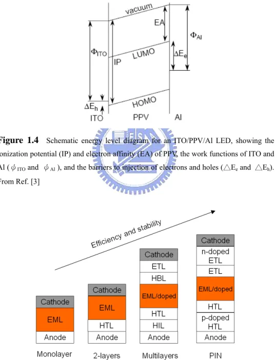
illustrated in Fig. 1.3. A schematic energy-level diagram for a PPV LED under forward bias is shown in Fig. 1.4. Based on these important findings, many companies and institutions start to pursuit display applications with organic materials. Research continues to focus on perfecting materials to produce better color, require less power and last longer. The key advantages of OLEDs for flat-panel display applications are their self-emitting property, high luminous efficiency, full color capability, wide viewing angle, high contrast, low power consumption, low weight, and flexibility.
The historical evolution of OLED architectures is shown in Fig. 1.5. Initially, a simple monolayer structure is utilized, as in Fig. 1.3. The ITO layer functions as a transparent electrode, and allows the light generated within the diode to leave the device. The top electrode is formed by thermal evaporation of a metal. Electroluminescence is achieved when the diode is biased sufficiently to achieve injection of positive and negative charge carriers from opposite electrodes. Recombination of oppositely charged carriers within the region of the polymer layer can then result in photon emission.
Since the breakthrough of the Kodak group, more and more layer layers have been used with various functions. As shown in Fig. 1.5, it has been demonstrated that the electroluminescence efficiency of OLEDs can be increased by carrier or exciton confinement within a multilayer device.[20] Another promising approach for low-power display technology is to combine electrically doped transport layers and a phosphorescent-doped emitting layer in a diode structure called a p-i-n junction.[21] Multilayer PLED made by solution process are also realized.[22]
Figure 1.3 Structure of a single-layer polymer electroluminescent diode. From Ref. [3].
Figure 1.4 Schematic energy level diagram for an ITO/PPV/Al LED, showing the ionization potential (IP) and electron affinity (EA) of PPV, the work functions of ITO and Al (ψITO and ψAl ), and the barriers to injection of electrons and holes (△Ee and △Eh).
From Ref. [3]
Figure 1.5 Evolution of organic light-emitting diode structures (HIL=hole injecting layer, HTL=hole transporting layer, EML=emitting layer, HBL=hole blocking layer, ETL=electron transporting layer).
grow to 10% or more by 2040. There are three main types of silicon solar cells in production: silicon wafer based, compound crystalline, and thin-film solar cells. Currently, crystalline silicon solar cells are the predominant technology which accounting for 80-85% of all cells manufactured. However, for silicon solar cells, significant fraction of the cost of solar cells comes from the photoactive materials and sophisticated processing technologies.
Recently, it has been shown that the inorganic materials utilized in solar cells can be replaced by semiconducting polymers which is capable of achieving reasonably high power conversion efficiencies. These polymers are inexpensive and can be solution-processed with high throughput. These organic solar cells could provide electricity at a lower cost than crystalline silicon solar cells if a reasonable power efficiency and lifetime could be achieved.
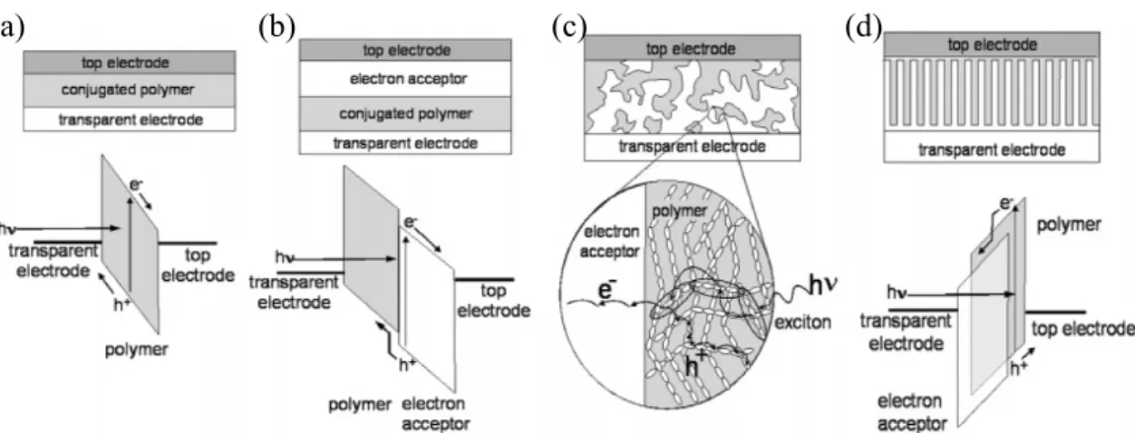
One of the first organic solar cells based on conjugated polymer is made by a spin coated polymer film sandwiched between two metal electrodes with different work functions, as shown in Fig. 1.6(a).[23] In most cases the open-circuit voltage was roughly equal to the work function difference between the top and bottom electrodes divided by the charge of an electron. Since the exciton diffusion length for most organic solar cell materials is below 20 nm, only those excitons generated in a small region within 20 nm from the contacts contribute to the photocurrent. Although single-layer solar cells are easy to fabricate, its photocurrent is very low.
Figure 1.6(b) shows a bilayer device, a donor and an acceptor material are stacked together with a planar interface. The bilayer is sandwiched between two
Figure 1.6 Four device architectures of conjugated polymer-based photovoltaic cells: (a) single-layer PV cell; (b) bilayer PV cell; (c) disordered bulk heterojunction; (d) ordered bulk heterojunction. From Ref. [24]
electrodes matching the highest occupied molecular orbital (HOMO) of donor and the lowest unoccupied molecular orbital (LUMO) of acceptor, for efficient extraction of the corresponding charge carriers.[25] The charge separation occurs in the interface which has a large potential drop between donor and acceptor. Upon photon absorption in the donor, excitons generated within a few nanometers of the heterojunction and excitons could diffuse to the interface. If an acceptor molecule is in close proximity, the electron may be transferred to the LUMO of acceptor. This process of forward charge transfer led to the spatial separation of the electron and hole, thereby preventing direct recombination and allowing the transport of electrons to one electrode and holes to the other. However, the carrier transit time to electrode is long if the organic layer is thick or the mobility of the organic material is low.
To circumvent the problem of low exciton diffusion length, the bulk heterojunction device is developed to intimately mix the donor and acceptor components in a bulk volume so that each donor–acceptor interface is within a distance less than the exciton diffusion length of each absorbing site.[26] The bulk heterojunction device is similar to the bilayer device with respect to the donor-acceptor concept, but it exhibits a largely increased interfacial area where (a) (b) (c) (d)
heterojunction requires percolated pathways for the hole and electron transporting phases to the contacts. Therefore, the bulk heterojunction devices are much more sensitive to the nanoscale morphology in the blend, which will be discussed in more detail below.
Another kind of bulk heterojunction solar cell that has recently received attention is the conjugated polymer-titania (TiO2) solar cell. Although TiO2 does not absorb
visible light, it indeed have some potential advantages as an electron-accepting material. The most attractive aspect of using TiO2 with a conjugated polymer in a
solar cell is the fact that the TiO2 can be patterned into a continuous network for
electron transport.[27,28] A continuous network for electron transport should allow a fairly high volume fraction of the conjugated polymer to be used in films, as long as the TiO2 and polymer can be structured so that excitons can be dissociated effectively.
Other reasons to use TiO2 are that it is nontoxic, many molecules can be attached to its
surface, and it has been used to make dye-sensitized solar cells with up to 10% power efficiency.
In solar cells made from conjugated polymers and TiO2, it is generally the case
that electrons are transported to the transparent bottom electrode. Similarly, holes are transported to the top electrode. In these cells it is advantageous to use a high-work-function metal such as gold as the top electrode to provide an ohmic contact to the HOMO of the polymer. Besides, the method of making a thin nanoporous TiO2 film and then filling it in with conjugated polymer has the advantage
1.2.3 Organic field-effect transistors
The beginning of the electronics age was marked by cathode ray tube, vacuum rectifier, and vacuum-tube triode. The triode, includes a grid between the anode and the cathode, transformed the rectifier into an amplifier, and made the radio communication and long-distance telephone come true. However, the vacuum-tube triode was fragile, slow, and difficult to miniaturize.
Replacing the triode with a solid-state device offering an alternative to the thermionic principle is thus a good idea for solving problems of triode. This concept was successfully demonstrated with Bardeen and Brattain’s point-contact transistor and Shockley’s bipolar transistor. After material technology research for more than forty years, the performance of metal-oxide-semiconductor field-effect transistor (MOSFET) is optimized. Today, MOSFETs dominated almost every electronic device.
Recently, organic field-effect transistors (OFETs) based on solution-processible polymeric as well as small molecular semiconductors have obtained impressive improvements in their performance. Even an all polymer transistor has been reported.[29] Initially, because of the poor performance of these initial devices, interest in organic transistors remained limited. Following a continuing effort, the carrier mobility was improved. Several review papers and books describing the materials, operating principles, and fabrication processes have been published for comprehensive understanding.[30-37]
Organic field-effect transistors have been developed to realize low-cost, large-area electronic devices. OFETs have been developed with various device geometries as depicted in Figure 1.7. The most commonly used device geometry is bottom gate with top contact partly because of using thermally grown Si/SiO2 oxide as
Figure 1.7 Schematic of the bottom-gate organic field-effect transistors with (a) top contact or (b) bottom contact structures. (c) Schematic diagram of a (c) top-gate with bottom contact transistor using a standard TFT device structures.
integration with organic light-emitting diodes. Another immediate opportunity is to use organic dielectric for the top-gate structured OFET. The solution for the organic dielectric can be properly chosen such that it will not destroy the underlying organic semiconductors. Top-gate bottom contact structure devices allow patterning the bottom source-drain electrodes on top of any flexible or rigid substrate first. Take the most commonly used OFET device configuration as example. The organic semiconductor is deposited on top of a dielectric with an underlying gate electrode. Current between source and drain electrodes is measured when no voltage is applied between the gate and source electrodes (off state). When a voltage is applied to the gate, electrons or holes can be induced at the semiconducor-dielectic interface and the source-drain current increases.
Carrier mobilities in organic semiconductors are limited by the hopping process between the molecules in disordered regions of the material. Many research works have examined the effects of modifying molecular parameters (regioregularity [38], molecular weight [39], and side-chain length [40]) and processing conditions (film thickness [41], doping level [42], thermal annealing [43], and the film-forming method [44]). Studies of semiconductor/insulator interface phenomena (such as surface-mediated molecular ordering, surface dipoles, semiconductor alignment using
Figure 1.8 (a) Crystallite structure in polythiophenes. The conjugation direction and the π-π stacking direction are fast charge transport directions. Charge transport in the alkyl stacking direction is slower. (b) Plane-on and (c) edge-on texture of polymeric crystallites. In the plane-on texture, the alkyl stacking direction is in the plane of the substrate, which is bad for the current density in TFTs. From Ref. [31]
self-assembled monolayers (SAMs), physical treatment, and photoalignment) are also receiving attention for enhancing the electrical properties of organic semiconductors. SAMs are highly ordered, two-dimensional structures that form spontaneously on a variety of surfaces. Tuning of the interfacial surface can be achieved by varying the rigidity, length, and terminal functional group of the molecule, which in turn affects the uniformity, packing, conformation, polarity, and charge density of the surface.
Fluorene copolymers and polythiophenes have a relatively rigid backbone with attached alkyl chains for solubility, and are able to crystallize. Mobility is highly anisotropic as a result of chain packing in the crystallites. Charge transport is fastest in the conjugation direction as shown in Fig. 1.8(a). When chains pack, the π-orbitals belonging to different polymer chains are stacked cofacially, and this partial overlap between π-orbitals assists interchain charge transfer. However, in another direction, the insulating alkyl chains impede charge transport so that mobility in this direction is the lowest. Such anisotropy has been experimentally verified by comparing the electrical characteristics of TFTs and diodes. Because of this pronounced anisotropy, texture and relative orientation of crystallites are expected to play an important role in controlling the electrical properties of these materials.
states (on/off ratio) and the field-effect mobility are two parameters to characterize the organic field-effect transistors. So far the organic FET shows low current output because of the intrinsically low carrier mobility due to the weak wavefunction overlaps between the molecules and the disorder in the thin film. The low mobility also strongly limits the operation speed to be under 100 kHz. Furthermore, the organic FET is unstable because the conduction channel is confined to a few monolayers at the semiconductor-dielectric interface where the adsorbed oxygen, moisture, and other chemicals have huge effect on the transistor characteristics. To obtain a desired current output, its operating voltage usually exceeds 20 volts. A great deal of effort was made in to improve the performance of the field-effect transistors by increasing the mobility, reducing the gate dielectrics thickness, and reducing the channel lengths.
For new material developments, many new organic molecules have been designed and synthesized.[45-51] Pentacene represents one of the most studied molecule for FET application. Under favorable fabrication conditions, mobilities as high as 5 cm2V-1s-1 have been reported.[45] Much progress has also been made in polymeric materials.[52,53] So far the highest mobility for polymer is about 1 cm2 V−1s−1.[52] While these values are still far below that offered by inorganic semiconductors, some are appropriate for some low-end applications. One way to reduce the operating voltage is utilizing a self-assembled monolayer (SAM) as gate dielectric with gate current densities as low as 10-9 Acm-2.[54,55] With these dielectrics, the transistor can be operated with voltages of 2 V. The devices is however sensitive to the pin-holes in SAM and not highly reproducible. Lithography
upon SAM is also difficult. Organic field-effect transistors with submicron channel lengths made by electron-beam lithography [56], nanoimprint lithography [57] and soft contact lamination [58] have been demonstrated. Vertical organic field-effect transistors, whose channel length was determined by the thickness of an insulating layer between source and drain, have been made by solid-state embossing [59], excimer laser [60] and photolithography [61]. However, these procedures to reduce the channel length are complicated and expensive. So far the organic FET still suffers from low mobility, high voltage and low speed. The unique promises of organic materials such as low-cost and large-area solution process not yet realized by high-performance field-effect transistors.
Vertical non-field-effect transistors with multilayer sandwich structures give another route to circumvent the limits of organic field-effect transistors. In vertical non-field-effect transistors, the channel length can be made small easily because of it is defined by the thickness of the organic layers. The current is modulated by a conductive metal layer embedded in the organic materials. Various device operating principles were proposed with different types of conductive layers such as a thin metal film [62,63], a strip-type metal film [64,65], a mesh gate electrode [66-685], and a porous conducting polymer network.[69] The remaining problems are the low current density, low on/off ratio as well as the complex fabrication process.
In order to tackle the major challenge for organic transistors, that is, low mobility of most organic materials, molecular or polymeric, we have invented two new metal-base organic transistors with vertical structure. One is based on the concept of hot carrier ballistic transport in the base [70,71], and another one is a solid-state analogy of vacuum tube which we call space-charge-limited transistor [72,73]. Operation principles and device structures of these two vertical metal-base organic transistors are discussed below. They show good performance including low voltage,
following chapters.
1.4 Overview of the thesis
The main theme of this thesis is the characterization of two metal-base transistors with vertical structure. A polymer light-emitting transistor, which is realized by vertically stacking a top-emitting polymer light-emitting diode on a polymer space-charge-limited transistor, is also characterized.
In Chapter 2, useful information which serves as a reference materials for the remainder of this thesis are provided. Physics of conjugated organic materials are reviewed in Section 2.1. How charge carriers inject into the materials through metal/organic interface and how charge carriers transport in the organic molecules are discussed in Section 2.2 and Section 2.3 respectively. For devices with opposite charged carriers, exciton formation and the luminous efficiency are introduced in Section 2.4. Other relevant devices and device physics are reviewed in Section 2.5. Many useful references are cited.
Polymer hot-carrier transistors with various emitter materials are discussed in Chapter 3. For the emitter material with high band gap, electrical properties and fabrication procedures are described in Section 3.2, while Section 3.3 discusses the hot-carrier transistors with low band gap emitter. The properties of the hot-carrier transistor with a blend polymer as emitter are described in Section 3.4. Optical response of a polymer light-emitting diode connected to the hot-carrier transistor are
also shown in Section 3.4
Polymer space-charge-limited transistors with different fabrication procedures and properties are discussed in Chapter 4. The electrical properties of the transistor with low opening density is described in Section 4.2, while Section 4.3 describe the electrical properties of transistor with high opening density. Fabrication procedure of the grid electrode is also described in detail.
Light-emitting polymer space-charge-limited transistor is described in Chapter 5. It is realized by vertically stacking a top-emitting polymer light-emitting diode on a polymer space-charge-limited transistor. Fabrication procedures, electrical response and optical response are discussed in Section 5.3 and Section 5.4 respectively.
In the final Chapter, the results of our experiments are concluded. Suggestions are also given for further studies on vertical metal-base transistors.
21
Theoretical background
We are interested in the invention and fabrication of novel organic devices with all kinds of operation principles. In this chapter, fundamental polymer physics and device physics required for this thesis are introduced. Section 2.1 introduces molecular orbital and electronic excitations. Information about the interface is discussed in Section 2.2. Section 2.3 discusses the charge injection and transport. After opposite charged carrier injected into the semiconductor, the formation of exciton and the quantum efficiency are discussed in Section 2.4. Operation principles of related devices are described in Section 2.5.
2.1 Semiconducting polymers
2.1.1 Molecular orbital and bonding
The bonding in organic semiconductors is fundamentally different from inorganic semiconductors. Organic molecular crystals are van der Waals bonded solids implying a considerably weaker intermolecular bonding as compared to covalently bonded semiconductors such as Si or GaAs. Polyacetylene (CH)n is
composed of a chain of repeating CH units. Since polyacetylene is the simplest polymer, it is used as an example here. Structures of trans-polyacetylene and
Figure 2.1 (a) Structures of trans-polyacetyelene. (b) The counterpart of trans-polyacetyelene with single and double bond exchanged. (c) Structures of cis-polyacetyelene. (d) The counterpart of cis-polyacetyelene with single and double bond exchanged.
cis-polyacetylene are shown in Fig. 2.1(a) and 2.1 (c), respectively. The structure of trans-polyacetylene and the structure obtained by interchanging the single and double bonds is energetically degenerate. While for the structure of cis-polyacetylene and the structure obtained by interchanging the single and double bonds, they are not energetically degenerate.
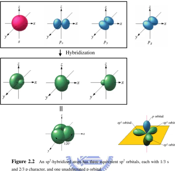
There are four valence electrons in carbon’s outer shell. Three of these electrons form a hybridized sp2 orbital, which is a linear combination of the spherical s orbital and two dumbbell shaped p orbitals as shown in Fig. 2.2. An sp2-hybridized atom has three equivalent sp2 orbitals, each with 1/3 s and 2/3 p character, and one unadulterated p orbital. The sp2 orbitals are 120° apart. Two of them form σ bonds with the two adjacent carbon atoms and the third bonds with the hydrogen atom. The trigonal planar nature of the sp2 orbitals gives trans-polyacetylene its zigzag backbone structure.
The fourth valence electron of each of the carbon atoms resides in a pz orbital
that is perpendicular to the plane of the sp2 orbitals. The electronic wavefunctions of the pz orbitals on adjacent carbons overlap and form the delocalized π bond as
(a)
(c)
(b)
Figure 2.2 An sp2-hybridized atom has three equivalent sp2 orbitals, each with 1/3 s and 2/3 p character, and one unadulterated p orbital.
Figure 2.3 Formation of σ bond and π bond.
shown in Fig. 2.3. The presence of the π electron is the important difference between conjugated polymers and non-conjugated polymers. Since the π band between the carbon atoms are weaker than σ bond, the orbitals appear at higher energies. The electrons in the σ bonds form the backbone of the chain while the π
Hybridization
σ-bonding
π-bonding
p
zFigure 2.4 The energy levels of a π-conjugated molecule. The lowest electronic excitation is between the bonding π–orbital and the antibonding π*–orbital.
electrons delocalize along the chain. The π electron delocalization and the weak interchain bonding give polyacetylene and other members of the class of conjugated polymer a quasi-one dimensional nature and give rise to strong anisotropies when the macromolecules are chain extended and chain aligned.
When atomic orbitals form molecular orbitals, these orbitals are often divided into bonding orbitals and antibonding orbitals as shown in Fig. 2.4. The lowest electronic excitations is between the bonding π -orbital and the antibonding π*-orbital. The σ bonds form completely filled low lying energy bands that have a much larger ionization potential than the π-electrons and thus do not contribute in a major way to the electrical or optical properties. As the intermolecular interaction is increased, the π and π* bands become broader, and the energy gap between the highest occupied molecular orbital (HOMO) and lowest unoccupied molecular orbital (LUMO) is lowered.
According to the Peierls’ Instability, the one-dimensional polyacetylene is unstable against a doubling of the unit cell which will lead to alternating bond lengths as well as to an energy gap. The chain of evenly spaced carbon atoms spontaneously distorts to a chain with alternating bond lengths, called a “dimerized” chain as shown in Fig. 2.5. The bond length alternates between single and double bonds. Dimerization
Figure 2.5 Period doubling in dimerized chain. From Ref. [74].
doubles the period of the lattice, making the HOMO completely filled. As a result, polyacetylene is a semiconductor. [74]
2.1.2 Electronic excitations
The electronic excitations in quasi-one-dimensional materials are different from those in conventional semiconducotrs. Assuming that a linear chain model without inter-chain interactions can be applied to polymers with degenerate ground state, two excitations are expected, namely the solitons and the polarons. In the case of polymers with non-degenerate ground state, the soliton is clearly not a stable excitation in these polymers, since the high-energy form can only exist over a finite length of chain. The charged excitations of a non-degenerate ground state polymer are termed polarons and bipolarons, which represent localized charges on the polymer chain with an accompanying local bonding rearrangement. However, if the inter-chain interaction has taken into account, then polarons may be unstable. Hence the excited carriers are expected to be electrons or holes as in conventional semiconductors.[75]
Solitons can be viewed as bond-alternation domain walls in trans-polyacetylene, and is illustrated for a neutral defect in Fig. 2.6. It separates a segment of polymer chain that alternates single bond, double bond; and a segment that alternates double bond, single bond. Trans-polyacetylene may or may not contain a soliton depending on the number of carbon atoms. The polymer chain contain an even number of carbon
Figure 2.6 Schematic form of a neutral soliton on a trans-polyacetylene chain. From
Ref. [76].
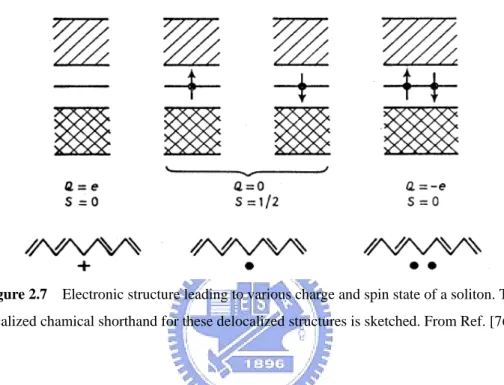
Figure 2.7 Electronic structure leading to various charge and spin state of a soliton. The
localized chamical shorthand for these delocalized structures is sketched. From Ref. [76].
atoms does not contain a soliton, while in odd-numbered chains a neutral soliton is incorporated for topological and energetic reasons. Thermal excitation will create additional solitons, but only in pairs on a chain. Upon doping either charged solitons or polarons are formed initially due to charge transfer from the dopant to odd chains and even numbered chains. The soliton can be neutral with spin 1/2 (one electron in the state at midgap) and charged positively or negatively with spin zero (corresponding to zero or two electrons in the midgap level) as shown in Fig. 2.7.
Formation of a polaron requires a sufficient separation between electron and hole so that they do not interact to form an exciton. When an electron is added to a conjugated polymer, the chain deforms around the charge in order to put the charge in a lower electronic energy state. The competition between elastic deformation energy and electronic energy determines the size of the lattice deformation. The added charge
Figure 2.8 Schematic energy band diagrams for polarons and bipolarons. From Ref.
[74].
on the polymer chain is thus not a free electron, but an electron that interacts with the polymer chain by deforming the chain around itself. The charge and the resulting deformation (phonon) constitute a polaron.[74] Polarons are formed similarly on all other conducting polymers.
Bipolarons are similar to polarons but they are doubly charged. Instead of being a single electron that distorts the lattice, there are two electrons or holes, with opposite spins, bound together within the same conjugation length. Although these electrons or holes repel one another via the Coulomb interaction, they remain bound together by their common lattice deformation.[77]
For the energy states located in the energy gap of the polymer as shown in Fig. 2.8. The polaron has two subgap states of which one is doubly occupied for a negatively charged polaron (P-) and the other is singly occupied for a positively charged polaron (P+). The doubly charged bipolaron has its subgap states either completely filled for a negative bipolaron (B2-) or completely empty for a positive bipolaron (B2+). A significant difference between polarons and bipolarons is their spin signatures. Polarons have charge ±1 and spin 1/2, while bipolarons are spinless and doubly charged.
2.2 Metal/organic interface
The choice of contacts in organic electronics is an area of critical importance. Unlike inorganic semiconductors, such as Si and GaAs, the Schottky energy barrier formed at a metal contact depends weakly on the choice of metal.[78] In organic transistors, contacts can affect the output current density. In organic electroluminescence devices, contacts can affect minority and majority current flow, and hence recombination rates and efficiency. In fact, the operation of organic light-emitting diodes depends on the asymmetry of the barrier heights at the two contacts. In this section, we consider some of the models adopt from inorganic semiconductor theory that have been used to describe the energy band diagram of a metal/organic structure.
2.2.1 Energy band diagram
When metal and n-type semiconductor are brought into contact, their Fermi levels must be equal at the interface in order to achieve thermodynamic equilibrium. In general, this requires a charge transfer between the metal and the semiconductor. Electrons from the semiconductor flow into the metal, leaving behind positive ionized donors in the semiconductor. The bands bend as shown in Fig. 2.9(b) and a Schottky barrier is formed. The band diagrams under different bias conditions are shown in Fig. 2.10. If p-type semiconductor is contact with metal, electrons are injected from the metal into the semiconductor, causing a build-up of negative charge in the semiconductor, and consequently the bands bend the other way. The barrier heights to electron and hole injection, φbn andφbp, can be calculated as follows:
(
m c)
n b e eφ = φ −χ (2.1) bn g p b E e eφ = − φ (2.2)Figure 2.9 (a) Energy band diagram of an isolated metal adjacent to an isolated n-type
semiconductor under thermal non-equilibrium condition. (b) Energy band diagram of a metal-semiconductor contact in thermal equilibrium. From Ref. [78].
Figure 2.10 Energy band diagrams of rectifying metal / n-type semiconductor contact
at (a) thermal equilibrium, (b) forward bias, and (c) reverse bias. From Ref. [78].
An ohmic contact can also be formed at a metal/semiconductor junction. One method is not to form a carrier injection barrier by use a metal with a work function which is smaller than that of the semiconductor for n-type semiconductors, or greater than that of the semiconductor for p-type semiconductors. However, this approach is not usually followed because the barrier height may be pinned by the high interface state density at the contact.[79] Another method is to use a heavily doped semiconductor at the interface to cause a significant band bending and a narrow
(b)
barrier for carrier tunneling through. However, for organic semiconductor, increase the free charge-carrier density by adding dopants is difficult. Therefore, so far, the common method is to minimize the barrier height by choosing appropriate contact materials.
2.2.2 Image-force lowering
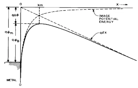
Image-force lowering is also known as the Schottky effect. It occurs in a metal/nonmetal interface. In such junctions, a barrier exists that controls the emission of carriers from the metal to nonmetal layer. The image force lowering reduces the barrier height, and a larger current flow may occur.
In simulations, the charge carrier injection barrier heights at the contacts are assumed to be field independent. However, in reality, this is not the case. The injection barrier height is reduced under applied bias due to the image force of the carrier as shown in Fig. 2.11. Consider a metal-vacuum system first. When an electron is at a distance x from the metal, a positive image charge will be induced on the metal surface. The force of attraction between the electron and the image charge is equivalent to the attractive force between the electron and the equal positive charge located at – x. The attractive image force, called the image force, is then given by the following expression:
( )
2 0 2 0 2 16 2 2 4 x q x q F πε ε π − = − = . (2.3) The potential energy of an electron at a distance x from the metal surface is given by:∫
∞ = = x e x q Fdx x U 0 2 16 ) ( πε . (2.4)When an external field E is applied, the total potential energy as a function of distance is given by: qEx x q x U = + 0 2 16 ) ( πε . (2.5)
Figure 2.11 The energy band diagram for the interface between a metal surface and a
vacuum. The metal work function is qφm. The effective energy barrier is lowered when
an electric field is applied to the surface. The lowering is due to the combined effects of the field and the image force. From Ref. [80].
The maximum barrier location xm
E q xm 0 16πε = cm (2.6)
The image force lowering Δφ:
0 3
4πε
φ = q E
Δ V. (2.7)
These results can also be applied to metal-semiconductor systems. In organic semiconductors, the free-space permittivityε0 should be replaced by an appropriate
permittivityεs characterizing the semiconductor medium. Hence, the Δφ:
s E q πε φ 4 3 = Δ V. (2.8)
In organic semiconductors, the values of εs around 3ε0 is much lower than
inorganic semiconductors. Therefore, the importance of image-force lowering term is increased. This contribution must be included for any device model to have a successful calculation.[81]
2.3 Carrier injection and transport
The theory of charge injection from a metal into an organic semiconductor and the carrier transport in organic semiconductor has been important topics for a long time. There are many theoretical research works available in the analysis of experimental data. Theoretical calculations based on different assumption and simplifications are not all suitable for organic materials. In this section we will review the commonly used formulations describing charge injection and transport in organic electronics.
Discussions are divided according to two limiting regimes of device operation, namely injection limitation and transport limitation of the current. The occurrence of maximum possible space-charge limited currents requires that at least one contact has good injecting properties. In contrast, injection limitation occurs if the injection barrier is so large that the injection current from the contact into the organic materials is insufficient to become the space-charge limited currents.
2.3.1 Injection limitation at the contact
There are two main possible mechanisms describing charge carrier injection, which are the thermionic emission and the tunnel emission. Both concepts are under certain conditions in inorganic semiconductors. The disorder in organic semiconductors poses an obstacle to be overcome. The process of injection into a disordered hopping system has been studied by many researchers, and these important references are cited for readers interested in this topic.
Thermionic emission
At any finite temperature T, the carrier density at any finite energy is not zero. There are always carriers above the barrier height. The thermally generated carriers
Where φb is the barrier height, kB is the Boltzmann constant, V is the applied voltage,
and A* is the effective Richardson constant. However, this calculation is not totally correct in the amorphous organic semiconductor where the electronic states are highly localized and charge transport is by hopping. For semiconductor with low mobility, it is necessary take into account the carrier diffusion within the barrier back toward the contact. The analysis is complicated, and depends on the type of barrier. Detail description can be found in Ref. [80], [81], and [82].
Tunnel emission
Tunnel emission, which is also called Fowler-Nordheim tunneling injection, is intrinsically quantum mechanical, with free carrier tunneling from states at the metal Fermi level directly into continuum stats through a triangular barrier. The current flow is described by . 2 4 3 2 exp * 2 / 3 2 2 2 2 * h m with qE k E q A J B B B π α αϕ α ϕ = ⎟⎟ ⎠ ⎞ ⎜⎜ ⎝ ⎛ − = (2.10)
E is the external field. The tunneling current can be analyzed by a Fowler-Nordheim plot, where log(J/E2) is plotted against 1/E to give a straight line. The gradient of the line can be used to extract the barrier height. The characteristic of field emission for a Schottky barrier is that the current strongly dependent on the applied field. The current expressions for the Schottky barrier and thermally assisted tunneling are complicated. Detail description can also be found in Ref. [80], [81], and [82].
2.3.2 Transport limitation in the bulk
As the contact is able to supply sufficient carrier density which is higher than the material has in thermal equilibrium without carrier injection, the total current will be limited by the space charge within the semiconductor. In this circumstance, the current is limited by the material properties rather than the contact. The space-charge-limited current has been treated in various situations.[83] Here, we introduce some results under different conditions.
In vacuum
The magnitude of the current density J is given by
v
J = ρ amp/m2 (2.11) where v is the drift velocity, and ρ is the charge density. Both v and ρ are functions of the distance from the origin. At the carrier injecting electrode, the velocity of the electrons is very small, and hence the charge density is very large. While at the carrier collecting electrode the velocity is a maximum, the charge density is a minimum. From the assumption that the initial velocity can be neglected, the velocity of the carrier at any point can be determined from the equation
eV mv2 =
2 1
. (2.12) Hence, from Eq. 2.12, the Poisson’s equation
[
]
2 1 2 1 0 2 / 1 0 0 2 2 ) / ( 2 − − = = = = V kV m e J v J dx V d ε ε ε ρ (2.13) where[
]
0 2 / 1 ) / ( 2 e m ε J k = . (2.14) Define dx dV y= (2.15)dV kV
ydy= −12 (2.18)
Equation 2.18 can be integrated to
1 2 1 2 2 2 kV C y + = . (2.19) Since V = 0 at the carrier injecting electrode, and y=dV/dx=0, the constant of integration C1 is zero. By taking the square root of Eq. 2.19, the equation becomes
4 1 2 1 2k V dx dV y= = (2.19) dx k dV V−14 =2 12 . (2.20)
This equation integrates to
2 2 1 4 3 2 3 4 C x k V = + . (2.21) Since V = 0 at x = 0, the constant of integration C2 is zero. Finally,
3 4 3 2 3 4 2 3 x k V ⎟ ⎠ ⎞ ⎜ ⎝ ⎛ = (2.22) 2 2 3 0 2 1 2 9 4 x V m e J ⎟ ε ⎠ ⎞ ⎜ ⎝ ⎛ = . (2.23) Therefore, the current varies as the three-half power of the potential. This equation can be used to describe the space-charge-limited current in vacuum diode. The space-charge-limited current dose not depends on the temperature or the work function of the carrier injecting electrode. The geometry of the tube and the potential applied will determine the maximum current under the condition that the electron supply from the electrode is sufficient.[84]
In trap-free materials with field-independent mobility
For a trap-free material without traps and intrinsic carriers, and while the diffusion current is neglected and the mobility is field-independent, the space-charge-limited current can be derived as below.
The drift current is given by
nE e
J = μ . (2.24) Start from the equation
n dx dE e s = ε (2.25) and from Eq. 2.24
E e J dx dE e s μ ε = (2.26) μ εs J dx dE E = (2.27) dx J EdE sμ ε = (2.28) This differential equation can be integrated to give
1 2 2 1 C x J E s + = μ ε . (2.29)
According to the boundary condition E(0) = 0, Eq. 2.29 becomes
x J E sμ ε = 2 2 1 (2.30)
( )
12 2 1 2 x J E s ⎟⎟⎠ ⎞ ⎜⎜ ⎝ ⎛ = μ ε . (2.30) Therefore 2 3 2 1 2 3 2 1 0 9 8 2 3 2 L J L J Edx V s s L ⎟⎟ ⎠ ⎞ ⎜⎜ ⎝ ⎛ = ⎟⎟ ⎠ ⎞ ⎜⎜ ⎝ ⎛ = =∫
μ ε μ ε (2.31) 3 2 0 3 2 8 9 8 9 L V L V J = εsμ = εrε μ (2.32) Equation 2.32 is referred to as the trap-free square law, the Mott-Gurney square law,The boundary condition E(0) = 0 leads to an infinitely high carrier density at the contact. The problem of infinite carrier concentration can be resolved by including the diffusion term, but this makes an analytic solution impossible. More discussion can be found in Ref. [85], [86], and [87].
In the very low applied voltage condition, the number of injected charge carriers is negligible compared to the number of thermally generated free carriers, the current is described by Ohm’s law
d V n q
J = μ (2.33) where d is the material thickness.
In materials with traps and field-independent mobility
If there is a single set of shallow traps situated at certain energy below the conduction band, the total charge is
t f ρ
ρ + (2.34) and the ratio θ is
t f f ρ ρ ρ θ + = (2.35)
The ρf and the ρt are free carrier density and trapped carrier density, respectively.
The θ is equal to the ratio of free carriers to the total number of carriers. The current density is given by
E
J =μρf . (2.36) Equations becomes
0 ε ε ρ ρ r t f dx dE = + (2.37) and hence 3 2 0 8 9 L V J = θεrε μ . (2.38) The existence of unfilled traps modifies the transport mechanism by capturing the injected carriers. More information can be found in Ref. [88].
However, if traps are distributed in energy, they will be gradually filled with increasing electric field. The current will increase faster than quadratic until all traps are filled. One of numerous calculations is the trap-charge limited current.[82,83,87]
( )
2 1 1 1 0 1 1 2 1 + + + ⎟ ⎠ ⎞ ⎜ ⎝ ⎛ + + ⎟⎟ ⎠ ⎞ ⎜⎜ ⎝ ⎛ + = ll l l t C d V l l l q N l q N J μ εε (2.39) Furthermore, if the injected charge density is high enough that the traps are completely filled, the density of charge in traps becomes negligible compared to the injected charge, and the trap-filled space-charge-limited current comes back to the trap-free value as shown in Eq. 2.32.In materials with traps and field-dependent mobility
There have been many calculation results discussing the energy distribution form of traps and field-dependent mobility on the current density. The commonly used energy distribution form is the Gaussian distribution and exponential distribution. One example is given here.
Considering the Poole-Frenkel mobility
kT q where F F eff πε β β μ μ = = exp( ) ) ( 0 (2.40)
and the trap-filling effect, that is the hopping-type mobility
) exp( ) ( 0 kT E E t t eff =μ − μ , (2.40)

![Figure 2.8 Schematic energy band diagrams for polarons and bipolarons. From Ref. [74]](https://thumb-ap.123doks.com/thumbv2/9libinfo/8386488.178461/39.892.217.674.116.338/figure-schematic-energy-band-diagrams-polarons-bipolarons-ref.webp)