國 立 交 通 大 學
電子工程學系 電子研究所
碩 士 論 文
含鍺摻雜氮化矽薄膜在非揮發性記憶體
應用之研究
Study on the Application of Ge-Incorporated
Silicon Nitride Thin Film for Nonvolatile
Memory
研 究 生 : 柳 星 舟
指導教授 : 曾 俊 元 博士
含鍺摻雜氮化矽薄膜在非揮發性記憶體
應用之研究
Study on the Application of Ge-Incorporated Silicon
Nitride Thin Film for Nonvolatile Memory
研 究 生: 柳 星 舟
Student:
Hsin-Chou
Liu
指導教授: 曾 俊 元 博士
Advisor:
Dr.
Tseung
Yuen
Tseng
國 立 交 通 大 學
電子工程學系 電子研究所
碩 士 論 文
A Thesis
Submitted to Department of Electronics Engineering & Institute of Electronics
College of Electrical Engineering and Computer Science
National Chiao Tung University
in Partial Fulfillment of the Requirements
for the Degree of
Master
in
Electronics Engineering
June 2006
Hsinchu, Taiwan, Republic of China
含鍺摻雜氮化矽薄膜在
非揮發性記憶體應用之研究
研 究 生: 柳 星 舟
指導教授: 曾 俊 元 博士
國 立 交 通 大 學
電子工程學系 電子研究所
摘要
對最廣為使用的非揮發性記憶體 ─ 快閃記憶體而言,通常會遇到兩個瓶 頸:一是在元件尺寸繼續微縮下之瓶頸,由於尺寸微縮後穿隧氧化層(或閘極氧化 層)之厚度亦隨之下降,如此雖可得到較快的讀寫速度,但電荷保存時間亦隨之下 降,故須在兩者之間取得平衡點;二是在多次讀寫後在穿隧氧化層品質容易劣化 而產生漏電路徑,一旦有一條產生,所有儲存在浮動閘極(floating gate)的電荷都會 經由此漏電路徑而全部流失掉。為了克服上述兩個瓶頸,主要有兩種改良的的方 法被提出,一是 SONOS 非揮發性記憶體,另一種是奈米晶體(量子點)非揮發性記 憶體。 在本文中,一個將前述兩種非揮發性記憶體結合之新記憶體首次被提出。利用矽鍺氮(SiGeN)三元薄膜來取代 SONOS 非揮發性記憶體中的氮化矽(Si3N4)薄
膜,並藉由一系列的熱處理後,使鍺量子點析出,並被氮化矽所包圍,如此便完 成了將兩種記憶體結合之新記憶體。由於鍺量子點及包圍鍺量子點之氮化矽皆可 儲存電荷,故新記憶體的記憶視窗比單純只有鍺量子點或氮化矽薄膜來得更為
十年的電荷保存時間。 此外,乾式氧化及水氣處理步驟在阻擋氧化層形成時所扮演的角色也有進一 步之探討。隨著乾式氧化的時間越長,更多的鍺原子會被析出並且聚集成核,因 此,在拉曼分析中鍺的訊號也就越強。由於水分子比氧分子小,故水分子比氧分 子 更 容 易 得 鑽 入 阻 擋 氧 化 層 (blocking oxide) 中 並 修 補 阻 擋 氧 化 層 中 的 懸 鍵 (dangling bands),所以,在乾式氧化後多加一個水氣處理的步驟則會改善阻擋氧化 層的品質與增強其強度。實驗中發現,30 分鐘短時間乾式氧化後再加上水氣處理 的元件,其抗漏電能力和 60 分鐘長時間乾式氧化的元件一樣好,故水氣處理步驟 的引入不僅可改善阻擋氧化層的品質,同時,更可大幅的縮減製程所需之時間。
Study on the Application of Ge-Incorporated
Silicon Nitride Thin Film for Nonvolatile
Memory
Student: Hsin-Chou Liu
Advisor: Dr. Tseung Yuen Tseng
Department of Electronic Engineering and Institute of Electronics
College of Electrical Engineering and Computer Science
National Chiao Tung University
Abstract
For nonvolatile semiconductor memories (NVSM), there are two limitations encountered at the present time. (1) The limited potential for continued scaling of the device structure: this scaling limitation stems from the extreme requirements on the tunnel oxide layer. To balance between program/erase speed and retention time, there is a trade-off between speed and reliability for the optimal tunnel oxide thickness. (2) The quality and strength of tunnel oxide (or tunnel dielectric) after plenty of program/erase cycles, once a leaky path has been created in tunnel oxide, all charges stored in the floating gate will be lost. Therefore, two approaches, the silicon-oxide-nitride-oxide-silicon (SONOS) and the nanocrystal nonvolatile memory devices, have investigated to overcome this oxide quality limit of the conventional floating gate NVSM.
SiGeN film is introduced to replace the nitride film in SONOS structure. After several different thermal processes, Ge in the SiGeN film will be segregated to form Ge nanodots embedded in the SiNx/SiON film. Because there are two charge-storage node sources, the nodes in Ge nanodots and in SiNx dielectric film, comparing to SONOS and Ge nanocystal NVMs, a larger memory window can be obtained. When a memory device has a larger memory window, it is easier to meet the requirement of 10-year retention. And, we hope this approach can improve the two limitations mentioned above.
Besides, the roles of dry oxidation and steam treatment during blocking oxide formation are also considered. With the extension of dry oxidation time, the Ge signal in Raman spectrum increases gradually because there are more Ge atoms to be segregated from the SiGeN film and more time for Ge atoms to nucleate. A 3-mintue steam treatment is performed after 30 minutes dry oxidation. Owing to its smaller size and lower activation energy than O2 molecules, H2O molecules are more permeable through
the blocking oxide and can passivate dangling bonds in the blocking oxide. The purpose of steam treatment is to strengthen the blocking oxide and improve its quality. The I-V characteristic of the sample after 30 minutes dry oxidation plus 3 minutes steam treatment is comparable with that after 60 minutes long term dry oxidation. The introduction of steam treatment can not only improve the blocking oxide quality but also reduce the thermal process duration from 60 minutes to 33 minutes.
誌謝
兩年時光匆匆地逝去,轉眼間就到了離別的時候了,在這段期間的師長朋友 們,在我的心中對你們總是抱著無限的感激。 首先,要特別感謝我的兩位指導教授,曾俊元教授與張鼎張教授。曾教授淵 博的學識以及圓融的處事態度,令學生獲益匪淺;張教授宏觀的看法及許多創新 的研究方法,令學生耳目一新,並且在做人處事及實驗研究上,不斷的給予學生 指導,令學生收穫良多。能夠師承兩位師長的指導,是學生莫大的福氣。 再者,要感謝交大奈米中心及國家奈米元件實驗室提供良好的實驗設備及環 境以及在實驗上一起奮鬥的學長及伙伴們:小鳴、炳宏、陳董、土撥、世青、國 王、大山、眾神、阿飛、緯仁、佳州、林博、阿貴、淵州以及所以 TCC group 的 成員,有你們的一起奮鬥與幫助,令我的實驗之路走的並不孤單。還有常常在路 邊攤把酒言歡的學長朋友們:國旭、小明、阿寬、紀文、小正、小杰、豬頭、元 均,每週一次的聚會是我消除壓力最佳的管道。謝謝你們,我的朋友,這一路上 的陪伴,豐富了我的人生。 要感謝的人實在太多了,或許在文字上會有所遺漏,但我心中對你們的感激 卻是永遠無法磨滅的! 最後,我要感謝辛苦拉拔我長大的外祖父母,扈林森先生與扈王根弟女士; 辛苦養育我、在學業上讓我自由揮灑的父母親,柳偉峰先生與扈采慈女士,以及 所有愛我、支持我的家人,你們是我最堅強的支柱,沒有你們,就沒有今天的我! 我愛你們! 星 舟 2006 年 6 月Contents
Chinese Abstract --- i
English Abstract ---iii
Acknowledgment --- v
Contents ---vi
Table Captions ---viii
Figure Captions ---ix
Chapter 1
Introduction
1.1 General Background --- 11.2 Motivation --- 4
1.3 Organization of This Thesis ---6
Chapter 2
Basics principle of nonvolatile memory
2.1Introduction ---112.2 Basic program mechanisms ---12
2.3 Basic erases mechanisms ---13
Chapter 3 Sample Structure and Thermal Process
3.1 Sample Structure---223.2 Thermal Process--- 23
Chapter 4 Experiment Results and Discussions
4.1 Electrical Characteristics --- 294.1.1 Comparing to Other Memories---31
4.2 Mechanism of Ge Nanocrystals Formation --- 32
4.2.1 Directly Oxidize SiGeN Layer as Blocking Oxide ---32
4.2.2 Oxidize Capped Amorphous Si Layer as Blocking Oxide ---33
4.3.1 Directly Oxidize SiGeN Layer as Blocking Oxide ---35 4.3.2 Oxidize Capped Amorphous Si Layer as Blocking Oxide---36
Chapter 5 Conclusions
5.1 Conclusions --- 79
References
---81Vita
---85Table Captions
Chapter 4
Table 4-1 Conditions of thermal process.
Table 4-2
The different bonds’ wave numbers of Fourier Transform Infrared Rays (FTIR) spectra.
Table 4-3 The different bonds’ wave numbers of Fourier Transform Infrared Rays (FTIR) spectra.
Figure Captions
Chapter 1
Fig. 1-1 The device structure of conventional nonvolatile semiconductor memory.
Fig. 1-2 The device structure of SONOS nonvolatile memory.
Fig. 1-3 The development of the gate stack of SONOS EEPROM memory devices. The optimization of nitride and oxide films has been the main focus in recent years.
Fig. 1-4 The energy band diagrams of the write/erase operation for a SONOS device.
Fig. 1-5 The device structure of nanocrystal (nano-dots) nonvolatile memory.
Chapter 2
Fig. 2-1 Energy band diagram of MONOS.
Fig. 2-2 (a) Positive gate voltage applied when use Fowler-Nordheim tunneling to program (b) Energy band representation of Fowler-Nordheim tunneling. Electron in poly-Si conduction band tunnel through the triangular energy barrier.
Fig. 2-3 Fig.ure 2-3 (a) Positive gate voltage and Positive drain voltage applied when use hot carrier injection to program (b) Energy band representation of hot carrier injection
Fig. 2-4 Schematic diagram sketching the possible MONOS erase mechanisms: electron tunneling through tunneling oxides (E1), electron emission in the nitride and subsequent tunneling through tunneling oxides (E2), hole tunneling into the nitride (H1), injection of hot holes into the nitride (H2).
Fig. 2-5 (a) Negative gate voltage applied when use Fowler-Nordheim tunneling to erase (b) Energy band representation of Fowler-Nordheim tunneling to erase.
Fig. 2-7 (a) Negative gate voltage and negative drain voltage applied when use hot hole injection to erase. (b) Energy band representation of hot hole injection to erase.
Chapter 3
Fig. 3-1 (a) Sample structure of sample I (b) Sample structure of sample II.
Fig. 3-2 The TEM diagram of sample I before thermal oxidation.
Fig. 3-3 The TEM diagram of sample II before thermal oxidation.
Fig. 3-4 The thermal process flow of sample I.
Fig. 3-5 The thermal process flow of sample II.
Chapter 4
Fig. 4-1 The C-V diagrams of sample I with (a) condition A and (b) condition B. Both diagrams are gate injection.
Fig. 4-2 The C-V diagrams of sample I with (a) condition C and (b) condition D. Both diagrams are substrate injection.
Fig. 4-3 The retention character of sample I with condition C (60 min dry oxidation).
Fig. 4-4 The de-trapping schematic plot of positive oxide trapped charges in tunnel oxide.
Fig. 4-5 The endurance character of sample I with condition C (60 min dry oxidation).
Fig. 4-6 The C-V diagrams of sample II with (a) condition A and (b) condition B. Both diagrams are gate injection.
Fig. 4-7 The C-V diagrams of sample II with (a) condition C and (b) condition D. Both diagrams are substrate injection.
Fig. 4-8 The retention character of sample II with condition D (30 min dry oxidation + 3 min steam treatment).
Fig. 4-9 The endurance character of sample II with condition D (30 min dry oxidation + 3 min steam treatment).
Fig. 4-10 The schematic plot of positive oxide trapped charges in the SiOx oxidized from SiGeN film.
Fig. 4-11 The C-V hysteresis of Ge nanocrystals embedded in SiO2 (Ge nanocrystal
only) nonvolatile memory proposed by T. C. Chang et al. [3.1]
Fig. 4-12 The C-V hysteresis of SONOS memory.
Fig. 4-13 The band diagrams of SONOS, Ge nanocrystal and SONOS+ Ge nanocrystal NVSMs.
Fig. 4-14 The Fourier Transform Infrared Rays (FTIR) spectra of sample I before and after thermal oxidation process.
Fig. 4-15 (a) The TEM diagram and (b) AES analysis of sample I before oxidation.
Fig. 4-16 (a) The TEM diagram and (b) AES analysis of sample I after 60 min oxidation.
Fig. 4-17 The Raman spectra of sample I before and after dry oxidation process. A peak of Ge crystal appeared after oxidation.
Fig. 4-18 The Raman spectra of sample I with (a) 30 min short term and (b) 60 min long term dry oxidation.
Fig. 4-19 The Fourier Transform Infrared Rays (FTIR) spectra of sample II before and after 60 min thermal oxidation process.
Fig. 4-20 (a) The TEM diagram and (b) AES analysis of sample II before oxidation.
Fig. 4-22 (a) The TEM diagram and (b) AES analysis of sample II after 60 min oxidation.
Fig. 4-23 The Raman spectrum of sample II with 30 min dry oxidation.
Fig. 4-24 The Raman spectra of sample II before and after dry oxidation process. A peak of Ge crystal appeared after oxidation.
Fig. 4-25 The Raman spectra of sample II with (a) 30 min short term and (b) 45 min longer term dry oxidation.
Fig. 4-26 The C-V hysteresis of sample I with four different conditions (a) A, (b) B, (c) C, (d) D.
Fig. 4-27 The I-V characteristics of sample I with four different conditions.
Fig. 4-28 (a)The TEM diagrams and (b) Auger Electron Spectroscopy (AES) analysis after oxidation with condition D (30 minutes dry oxidation plus 3 minutes steam treatment).
Fig. 4-29 The Raman spectra of sample I after 30 min dry oxidation with and without 3 min steam treatment.
Fig. 4-30 The Raman spectra of sample I after 60 min dry oxidation with and without 3 min steam treatment.
Fig. 4-31 The C-V hysteresis of sample II with four different conditions (a) A, (b) B, (c) C, (d) D.
Fig. 4-32 The I-V characteristics of sample I with four different conditions.
Fig. 4-33 The TEM diagrams of (a) 60 minutes dry oxidation and (b) 30 minutes dry oxidation plus 3 minutes steam treatment.
Fig. 4-34 (a) The TEM diagrams and (b) Auger Electron Spectroscopy analysis after oxidation with condition D (30 minutes dry oxidation plus 3 minutes steam treatment)
3 min steam treatment.
Fig. 4-36 The Raman spectra of sample II after 60 min dry oxidation with and without 3 min steam treatment.
Chapter 1
Introduction
1.1 General Background
In 1967, D. Kahng and S. M. Sze invented the floating-gate (FG) nonvolatile semiconductor memory (or flash memory) at Bell Labs [1.1]. To date, the flash memory device structure, as shown in Fig. 1-1, continues to be the most prevailing nonvolatile-memory implementation, and is widely used in both standalone and embedded memories. The invention of flash memory creates a huge industry of portable electronic devices such as cellular phones, digital cameras, digital voice recorders, MP3 walkman, personal data assistants to compact smart cards, USB flash personal disc etc.
Although a huge commercial success, conventional FG devices have their limitations. Two of the most prominent limitations are: (1) the limited potential for continued scaling of the device structure. This scaling limitation stems from the extreme requirements put on the tunnel oxide layer. The tunnel oxide must be thin enough to allow quick and efficient charge transport to and from FG. On the other hand, the tunnel oxide needs to provide superior isolation under retention, endurance, and disturbed conditions in order to maintain information integrity over periods of up to a decade. When the tunnel oxide is thinner for operation speed consideration, the retention characteristics may be degraded. And when the tunnel oxide is made thicker to take the isolation into account, the speed of the operation will be slower. Therefore, for mass production, there is a trade-off between speed and reliability for the optimal tunnel oxide thickness. (2) the quality and strength of tunnel oxide (or tunnel dielectric) after
plenty of program/erase cycles. Once a leaky path has been created in tunnel oxide, all the charges stored in the floating gate will be lost. Therefore, two suggestions, SONOS [1.2-1.4] and nanocrystal nonvolatile memory devices [1.5-1.7], are proposed to overcome this oxide quality limit of the conventional FG structure. These technologies replace the floating gate structure with a great number of charge-storage nodes in the dielectric or in the nanocrystal. Unlike the floating gate, stored charges in isolated nodes cannot easily redistribute amongst themselves and the local leaky path will not cause the fatal loss of information for the nanocrystal nonvolatile memory device. This effectively prevents the leakage of all the stored charges out of the floating gate.
1.1.1 SONOS nonvolatile memory devices
SONOS (silicon-oxide-silicon-oxide-silicon) nonvolatile memory devices structure shown in Fig. 1-2, the charge storage elements in SONOS memory are the charge traps distributed throughout the volume of the Si3N4 layer. A typical trap has a density of the
order 1018-1019 cm-3 according to Yang et al [1.8] and stores both electrons and holes (positive charges) injected from the channel.
Figure 1-3 illustrates the progression of device cross section, which has led to the present SONOS device structure. The nitride-base memory devices were extensively studied in the early 70s after the first metal-gate nitride device MNOS (Metal/Nitride/Oxide/Silicon) was reported in 1967 by Wegener et al [1.9]. Initial device structures in the early 1970s were p-channel metal-nitride-oxide-silicon (MNOS) structures with aluminum gate electrodes and thick (45 nm) silicon nitride charge storage layers. Write/erase voltages were typically 25-30 V. In the late 1970s and early 1980s, scaling moved to n-channel SNOS devices with write/erase voltages of 14-18 V. In the late 1980s and early 1990s, n- and p-channel SONOS devices emerged with
between the gate and the nitride region. Thus, it forms the ONO (SiO2/Si3N4/SiO2) gate
dielectric stack (Fig. 1-2) instead of capping the nitride layer with just a metal or semiconductor gate. The purpose of the top blocking oxide is to reduce the charge injection from the control gate into the nitride layer, limiting the memory window of both MNOS and SNOS devices.
The program/erase mechanism is shown in Fig. 1-4. During programming, the control gate is biased positively so that electrons from the channel can tunnel across the SiO2 into the nitride layer. Some electrons will continue to move through the nitride
layer then across the control oxide finally into the control gate. The remaining trapped charges in the nitride layer provide the electrostatic screening of the channel from the control gate. Therefore, there is a threshold voltage (VT) shift resulting from trapped
charges in nitride and because of that SONOS can be used as a memory device just like conventional floating gate devices.
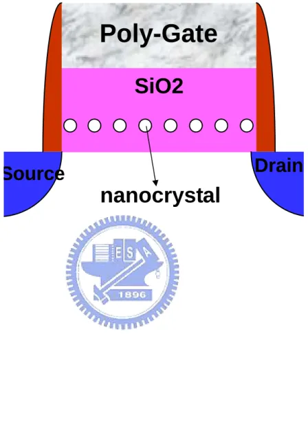
1.1.2 Nanocrystal nonvolatile memory devices
Nanocrystal nonvolatile memories, shown in Fig. 1-5, are one particular implementation of storing charges by dielectric-surrounded nanodots, and were first introduced in the early 1990s by IBM researchers who proposed flash memory with a granular floating gate made from silicon nanocrystals [1.10], In a nanocrystal NVSM (nonvolatile semiconductor memory) device, charge is not stored on a continuous FG poly-Si layer, but instead on a layer of discrete, mutually isolated, crystalline nanocrystals or dots. Each dot will typically store only a handful of electrons; collectively the charges stored in these dots control the channel conductivity of the memory transistor.
As compared to conventional stacked gate NVSM devices, nanocrystal charge storage offers several advantages, the main one being the potential to use thinner tunnel
oxide without sacrificing nonvolatility. This is a quite attractive proposition since reducing the tunnel oxide thickness is a key to lowering operating voltages and/or increasing operating speeds. This claim of improved scalability results not only from the distributed nature of the charge storage, which makes the storage more robust and fault-tolerant, but also from the beneficial effects of Coulomb blockade [1.11]. Quantum confinement effects (bandgap widening; energy quantization) can be exploited in sufficiently small nanocrystal geometries (sub-3 nm dot diameter) to further enhance the memory’s performance.
Due to the less drain to FG coupling, nanocrystal memories suffer less from drain induced barrier lowering (DIBL). One way to exploit this advantage is to use a higher drain bias during the read operation, thus improving memory access time. Of particular importance is the low capacitive coupling between the external control gate and the nanocrystal charge storage layer. This does not only results in higher operating voltages, thus offsetting the benefits of the thinner tunnel oxide, but also removes an important design parameter (the coupling ratio) typically used to optimize the performance and reliability tradeoff.
Unlike volume distributed charge traps (ex: nitride in SONOS NVM), nanocrystals be deposited in a two-dimensional 2-D) layer at a fixed distance from the channel separated by a thin tunnel oxide (Fig. 3). By limiting nanocrystals deposition to just one layer and adjusting the thickness of the top blocking dielectric, charge leakages to the control gate from the storage nodes can be effectively prevented.
for Semiconductors (ITRS) indicates the difficult challenge, beyond the year 2005, for nonvolatile semiconductor memories is to achieve reliable, low-power, low-voltage performance [1.12]. For nonvolatile flash memories, two limitations encountered at the present time are: (1) the limited potential for continued scaling of the device structure. This scaling limitation stems from the extreme requirements put on the tunnel oxide layer. In order to get balance between program/erase speed and retention time, there is a trade-off between speed and reliability to get the optimal tunnel oxide thickness. (2) the quality and strength of tunnel oxide (or tunnel dielectric) after plenty of program/erase cycles. Once a leaky path has been created in tunnel oxide, all the charges stored in the floating gate will be lost. Therefore, two suggestions, the SONOS and the nanocrystal nonvolatile memory devices, are proposed to overcome this oxide quality limit of the conventional FG structure. These technologies replace the floating gate structure with a great number of charge-storage nodes in the dielectric or in the nanocrystal. Unlike the floating gate, the local leaky path will not cause the fatal loss of information for the nanocrystal nonvolatile memory device. This effectively prevents the leakage of all the stored charges out of the floating gate.
In this thesis, a combination of SONOS and nanocrystal nonvolatile memory devices is proposed. A SiGeN film is introduced to replace the nitride film in SONOS structure. After several different thermal processes, Ge in the SiGeN film will be segregated to form Ge nanodots embedded in the SiNx (or SiON) film. Because there are two charge-storage node sources, the nodes in Ge nanodots and in SiNx dielectric film, comparing to SONOS and Ge nanocystal NVMs, a larger memory window can be obtained. When a memory device has a larger memory window, it is easier to meet the requirement of retention of 10 years. And, hope to solve the two limitations mentioned above.
1.3 Organization of This Thesis
In chapter 1, general background of flash nonvolatile memory, SONOS nonvolatile
memory and nanocrystal nonvolatile memory devices is introduced.
In chapter 2, basics of program and erase operation are introduced.
In chapter 3, sample structure, experimental methods and experimental process flow
are stated.
In chapter 4, discuss the SiNx:Ge memory electric characteristics, reliabilities,
mechanism of Ge dot formation in SiGeN film and role of steam treatment.. Finally, the conclusion is presented in chapter 5
Fig.1-1 The device structure of conventional nonvolatile semiconductor
memory.
Fig.1-2 The device structure of SONOS nonvolatile memory.
Poly-Gate
Nitride
Source Drain
SiO
2SiO
2Poly-Gate
Floating Gate
Source Drain
SiO
2SiO
2Figure 1-3 The development of the gate stack of SONOS EEPROM
memory devices. The optimization of nitride and oxide films has been the
Figure 1-4 The energy band diagrams of the write/erase operation for a
SONOS device.
Figure 1-5 The device structure of nanocrystal (nano-dots) nonvolatile
memory.
Poly-Gate
Drain
Source
SiO2
nanocrystal
Chapter 2
Basics principle of nonvolatile memory
2.1 Introduction
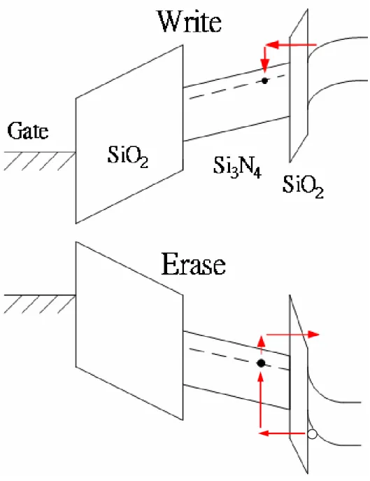
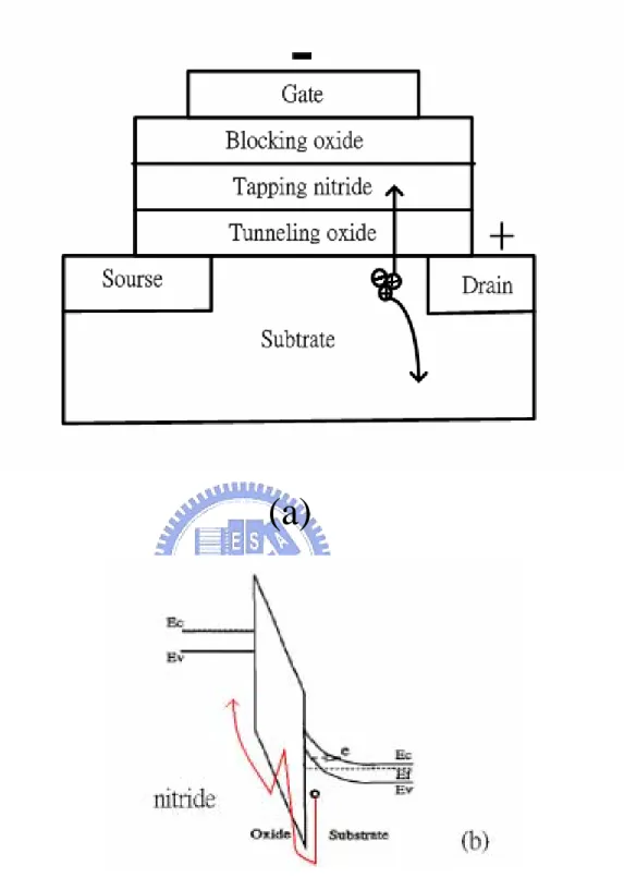
For SONOS NVSM, the basics operating principle of ONO structure is that electrons injected from the channel are trapped in the forbidden gap of the silicon nitride film during the program operation. On the other hand, during the erase operation, holes are injected from the substrate into silicon nitride film. If there are charges stored in the silicon nitride film, the threshold voltage can be modified to switch between two distinct values. [2.1]
The relation between bias and energy band bending is a key to understand basics program and erase mechanisms. Fig 2-1 shows energy band diagram of MONOS. The barrier of SiO2 is about 3.1 eV for electrons in the conduction band of silicon, and 4.78
eV for holes in valance band. The barrier of Si3N4 is about 1.05 eV for electrons in the
conduction band of nitride, and 2.85 eV for holes in valance band, the gap for electron between conduction band and trapping level is 0.7 eV, and, for hole between valance band and trapping level is 0.95 eV.
In this chapter, we will discuss program and erase mechanisms from the relation between bias and energy band bending. Fowler-Nordheim Tunneling, hot electron injection, band to band assisted hole injection, channel hole injection will be discussed briefly.
2.2 Basic program mechanisms
2.2.1 Fowler-Nordheim Tunneling
Fowler-Nordheim tunneling is a field-assisted carrier tunneling mechanism [2.2], when a large positive voltage is applied across a metal-ONO-substrate structure, its band stricture will be influenced as indicated in figure 2-2. Due to high electrical field, electrons in the poly-Si conduction band as triangular energy barrier with a width dependent on applied electric field. At sufficient high fields, the width of barrier becomes small enough to tunnel through the barrier from the poly-Si conduction band into nitride electron trap layer.
2.2.2 Hot electron injection
At large drain bias, the minority carriers that flow in the channel are heated by the large electric fields occurred at the drain side of the channel and their energy distribution is shifted higher. This phenomenon gives rise to impact ionization at the drain, by which both minority and majority carriers are generated. The highly energetic majority carriers are normally collected at the substrate contact and from the so-called substrate current. The minority carriers heating occurs when some of the minority carriers gain enough energy to allow them to surmount the SiO2 energy barrier. If the
oxide field favors injection, these carriers injected over the barrier into the gate insulator and give rise to the so-called hot-carrier injection gate current [2.3-2.4]. Figure 2-3 shows the phenomenon of hot electron injection. This mechanism is schematically represented for the case of an n-channel nonvolatile memory.
Vdsat (Vd > Vdsat), the mode can named hot carrier effect. To distinguish from Fowler-Nordheim tunneling, the definition of hot carrier injection in this study is the only condition that the drain is applied bias.
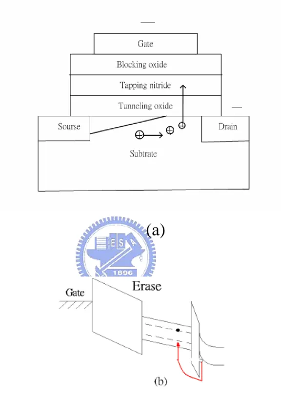
2.3 Basic erases mechanisms
There are three physical mechanisms that can be potentially responsible of erase method in nonvolatile memory with ONO structure, as indicated in figure 2-4. (1) electron escape from the nitride by tunneling through top and bottom oxides; (2) tunneling of holes generated by band-to-band into the nitride layer; and (3) the injection into the nitride of hot holes [5]. Electron almost can’t escape from the nitride for the nitride deep trap. Holes injection is the dominate mechanism in erase operation. In this study, we’ll discuss erase operation from this view.
2.3.1 Fowler-Nordheim Tunneling
Fowler-Nordheim tunneling is a field-assisted electron tunneling mechanism, when a large negative voltage is applied across a metal-ONO-substrate structure, its band stricture will be influenced as indicated on Figure 2-5. Due to high electrical field, holes in the poly-Si valance band as triangular energy barrier with a width dependent on applied electric field. At sufficient high fields, the width of barrier becomes small enough to tunnel through the barrier from the poly-Si valance band into nitride hole trap layer.
2.3.2 Band to band assisted hole injection
to the cell, electron-hole pairs are generated by BTBT in the drain region [2.6, 2.7]. The holes are accelerated by a lateral electric field toward the channel region and some of them obtain high energy. The injection of such hot holes [2.8] into nitride through the tunnel oxide is used for a new erase operation in N-channel.
2.3.3 Hot hole injection
The mechanism of hot hole injection in P-channel is like to hot electron injection. Figure 2-7 shows the phenomenon of hot hole injection. It’s reported that hole injection is a erase operation in P-channel device [2.9].
(a)
Figure 2-2 (a) Positive gate voltage applied when use Fowler-Nordheim tunneling to program (b) Energy band representation of Fowler-Nordheim tunneling. Electron in poly-Si conduction band tunnel through the triangular energy barrier.
(a)
Figure 2-3 (a) Positive gate voltage and Positive drain voltage applied when use hot carrier injection to program (b) Energy band representation of hot carrier injection
Figure 2-4 Schematic diagram sketching the possible MONOS erase mechanisms: electron tunneling through tunneling oxides (E1), electron emission in the nitride and subsequent tunneling through tunneling oxides (E2), hole tunneling into the nitride (H1),
(a)
Figure 2-5 (a) Negative gate voltage applied when use Fowler-Nordheim tunneling to erase (b) Energy band representation of Fowler-Nordheim tunneling to erase.
(a)
Figure 2-6 (a) Negative gate voltage applied when use band-to-band assisted injection to erase (b) Energy band representation of band to band assisted hole injection to erase.
(a)
Figure 2-7 (a) Negative gate voltage and negative drain voltage applied when use hot hole injection to erase. (b) Energy band representation of hot hole injection to erase.
Chapter 3
Sample Structure and Thermal Process
3.1 Sample Structure
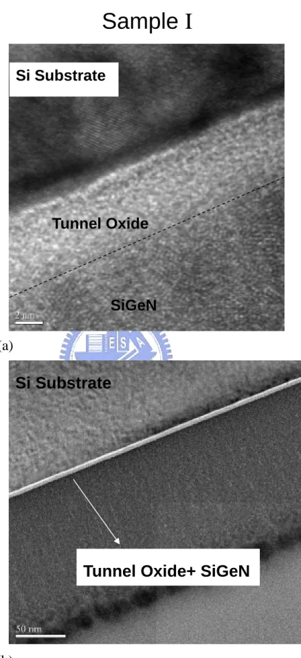
Figure 3-1 (a) and (b) show the two different pre-thermal sample structures, labeled as sample I and sample II, in this experiment. The transmission electron microscope (TEM) diagrams are shown in Fig. 3-2 and Fig. 3-3.
First, a 5-nm thermal oxide was grown on p-type Si substrate by dry oxidation in an atmospheric pressure chemical vapor deposition (APCVD) furnace as a tunnel oxide in both samples. Subsequently, in sample I: a 50-nm PECVD SiGeN was deposited on tunnel oxide; in sample II: a 20-nm PECVD SiGeN was deposited on tunnel oxide as charge-trapping layers, followed by the deposition of 20-nm PECVD a-Si layer.
The deposition of the PECVD SiGeN was kept at 200 ℃ in a low pressure of 6 mTorr with SiH4 : GeH4 : NH3 : N2 = 20 sccm : 5 sccm : 30 sccm : 500 sccm and a RF
power of 20 W. The N2 gas was served as the carrier gas to adjust the chamber pressure
and make the process gas can easily transport into the process chamber. The low pressure of 6 mTorr during deposition makes the mean free path of electrons and radicals increase, which will improve the uniformity of the thin film [3.1]. The sequent deposited a-Si was at 200 ℃ with SiH4 : H2 = 20 sccm : 980 sccm, and a 20W power.
Then, the samples were oxidized in thermal furnace at 900 ℃ in oxygen ambient to form blocking oxide. Besides, a three minutes steam treatment is performed on some
to form a metal/oxide/nitride/oxide/silicon (MONOS) structure.
In short, the difference between sample I and sample II is the thickness of SiGeN layer (thicker in sample I) and with/without capped amorphous Si layer (with Si cap layer in sample II).
3.2 Thermal Process
Fig. 3-4 and Fig. 3-5 indicate the thermal process flow in sample I and sample II. In sample I, directly oxidize a thick SiGeN layer (sample I) to form blocking oxide by a dry oxidation process with different time or by a 30 min dry oxidation process followed by a 3 minutes steam treatment in thermal furnace at 900 ℃. In sample II, oxidize the amorphous Si layer capped on the SiGeN layer(sample II) to form blocking oxide by a dry oxidation process with different time or by a 30 min dry oxidation process followed by a 3 minutes steam treatment in thermal furnace at 900 ℃. The steam treatment means let in H2O into thermal furnace, the same as wet oxidation. Owing to its smaller
size and lower activation energy than O2 molecules, H2O molecules are more permeable
through the blocking oxide and can passivate dangling bonds in the blocking oxide. The purpose of steam treatment is to strengthen the blocking oxide and improve its quality.
Figure 3-1 (a) Sample structure of sample I (b) Sample structure of sample
II.
Si-substrate
Tunnel ox. 50A
SiGeN
(a)
Sample I
Si-substrate
Tunnel ox. 50A
SiGeN
a-Si
Sample II
Sample I
(a)
(b)
Figure 3-2 The TEM diagram of sample I before thermal oxidation.
Si Substrate
SiGeN
Tunnel Oxide
Tunnel Oxide+ SiGeN
Si Substrate
Sample II
Si Substrate
Tunnel Oxide
SiGeN
a-Si
Tunnel Oxide
SiGeN
Si Substrate
a-Si
Directly Oxidize SiGeN Layer to Form Blocking Oxide
Figure 3-4 The thermal process flow of sample I.
Si-substrate
Tunnel ox. 50A
SiGeN
Si-substrate
a-Si
200A
Blocking ox.
Ge dot
Tunnel ox. 50A
SiON
Thermal
Oxidation
•
Dry
•
Dry + steam treatment
Oxidize The Amorphous Si Layer Capped on the
SiGeN layer to Form Blocking Oxide
Si-substrate
Tunnel ox. 50A
SiGeN
a-Si
Si-substrate
a-Si
200A
Blocking ox.
Tunnel ox. 50A
SiON
Thermal
Oxidation
•
Dry
•
Dry + steam treatment
Ge dot
Chapter 4
Experiment Results and Discussions
4.1 Electrical Characteristics
In previous section, it has been mentioned that there are two methods used to form blocking oxide. In one method, only a dry oxidation process with different time in thermal furnace at 900 ℃ is adopted. In the other method, a dry oxidation process is followed by a 3 minutes steam treatment. Table 4-1 shows the difference conditions performed on sample I and sample II. The Ge nanocrystals embedded SiON layer (the charge storage layer) of a MOIOS memory device is utilized to capture the injected carriers from the channel. When the device is programmed, electrons directly tunnel from the Si substrate through the tunnel oxide by Fowler-Nordheim (F-N) tunneling. The tunneling electrons are trapped in the forbidden gap of SiON layer and conduction band of Ge nanocrystals in the SiON layer. For the erasion, the holes may tunnel from the valence band of the Si substrate. The tunneling hole recombine with the electrons trapped in the forbidden gap of SiON layer and conduction band of Ge nanocrystals in the SiON layer. The blocking oxide is utilized to prevent the carriers of gate electrode from injecting into the charge-trapping layer by Fowler-Nordheim (F-N) tunneling. The capture of carriers will causes a variation in the threshold voltage and can serve as a memory device.
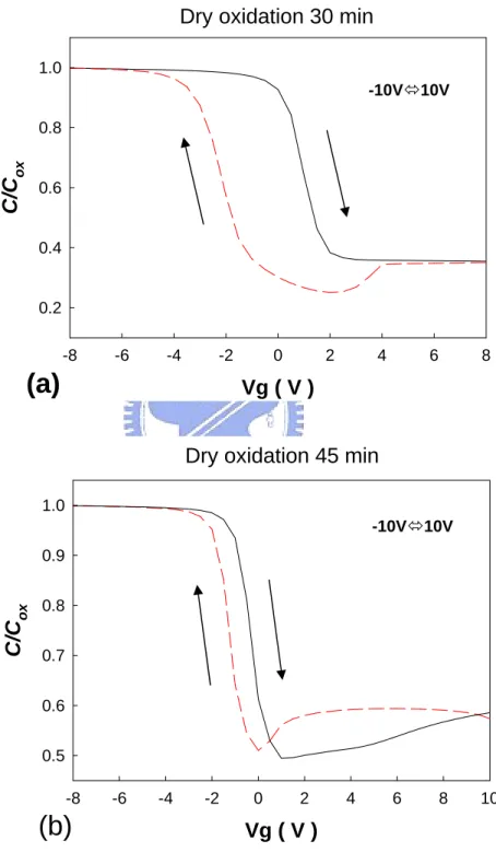
The capacitance-voltage (C-V) hysteresis of sample I (without capped Si layer) with three different conditions A, B, C and D are shown in Fig. 4-1 (a), (b) and Fig. 4-2 (a), (b), respectively. In 30 and 45 minutes short term dry oxidation (condition A and B),
because the thickness is not thick enough and the quality is not good enough, the blocking oxide can’t block the carriers (electrons or holes) tunneling from gate to charge storage layer. When the dry oxidation time is extended to 60 minutes (condition C), the blocking oxide is thick enough to block the carriers from gate and therefore the way carrier injection turns from gate injection to substrate injection. In condition C, the memory windows are ~1.1V under ±3V C-V sweeping, ~2.4V under ±5V C-V sweeping and ~4V under ±7V C-V sweeping. In condition D (30 minutes dry oxidation followed by 3 minutes steam treatment), the memory window is 0.9V under ±10V C-V sweeping. The retention character of sample I with condition C (60 minutes dry oxidation) is shown in Fig. 4-3. The program curve and erase curve in Fig. 4-3 shift toward positive voltage at the same time because positive oxide trapped charges are created during the program/erase cycles in tunnel oxide and they will de-trap with the retention time [4-1]. As the de-trapping of the positive oxide trapped charges, the threshold voltage will shift to positive side. The schematic plot and are shown in Figure 4-4. The endurance characteristic of sample I with condition C (60 minutes dry oxidation) is shown in Fig. 4-5. There is almost no shift in the threshold voltage after 106 program/erase cycles under ±3V operation.
The capacitance-voltage (C-V) hysteresis of sample II (with capped Si layer) with four different conditions A, B, C and D are shown in Fig. 4-6 (a), (b), and 4-7 (a), (b), respectively. The C-V properties are of the same trends as sample I. In 30 and 45 minutes short term dry oxidation (condition A and B) a gate injection is observed. Also, substrate injections are observed in 60 minutes dry oxidation (condition C) and 30 minutes dry oxidation plus a 3-minute steam treatment (condition D). In condition C, the threshold-voltage shift (memory window, ∆Vt) under ±7V C-V sweeping is ~1.7 V
sweeping and ~4.2V under ±10V C-V sweeping. The retention and endurance character of sample II with condition D are shown in Fig. 4-8 and Fig. 4-9. The Auger Electron Spectroscopy (AES) analysis of sample II with condition D is shown in Fig. 4-33 (b). There is a rise in oxygen signal after steam treatment in AES analysis. The SiON dielectric is oxidized by steam to form SiOx. As a result, the Ge nanocrystals are not embedded in SiON but in SiOx. The program and erase curves in Fig. 4-9 shift to negative voltage at the same time because positive oxide trapped charges are created during the program/erase cycles in both tunnel oxide and the SiOx oxidized from SiON film by steam treatment [4-1]. The schematic plot is shown in Figure 4-10. The positive trapped charges in SiOx oxidized from SiON film will increase with the P/E cycles because of its worse quality than tunnel oxide’s. Therefore, the threshold voltage in the Fig. 4-9 will shift to negative side.
4.1.1 Comparing to Other Memories
Figure 4-11 shows the C-V hysteresis of Ge nanocrystals embedded in SiO2 (Ge
nanocrystal only) nonvolatile memory proposed by T. C. Chang et al. [4.2]. Fig. 4-12 shows the C-V hysteresis of SONOS memory and the SiNx layer in the ONO stack is deposited by the same PECVD used in this study. The memory windows in the Ge nanocrystal only NVSM are ~0.4V under ±5V C-V sweeping and ~2V under ±10V C-V sweeping. The memory windows in SONOS only NVSM are ~0.2V under ±5 C-V sweeping and ~0.6V under ±10V C-V sweeping. In this study, a combination of Ge nanocrystal and SONOS NVSM is proposed. The memory windows of sample I with condition C are ~1.1V under ±3V C-V sweeping, ~2.4V under ±5V C-V sweeping and ~4V under ±7V C-V sweeping, as shown in Fig. 4-2 (a). Moreover, The memory windows of sample II with condition D are ~0.6V under ±3V C-V sweeping, ~1.8 V under ±7V C-V sweeping and ~4.2V under ±10V C-V sweeping, as shown in Fig. 4-7 (b). The memory windows both in sample I and sample II are larger than Ge nanocrystal
only NVSM or SONOS only NVSM (table. 4-4) and even larger than the Ge nanocrystal NVSM plus SONOS NVSM. It’s inferred that besides charge trapping units in the Ge nanocrystal and the SiON dielectric, there are additional charge trapping units at Ge/SiON interface. The band diagrams are shown in Figure 4-13.
4.2 Mechanism of Ge Nanocrystals Formation
Kan et al. adopted a two-step RTA process executed on a Si0.54Ge0.46 film to form
Ge nano-dots embedded in SiOx dielectric [4.3-4.4] and the 950 N℃ 2 RTA would
reduce the Ge atoms and the nanocrystals grew based on the Ostwald ripening mechanism [4.5]. Besides, a method of Ge nano-dots segregated downward until they reach the tunnel oxide surface by Si0.8Ge0.2 layer being wet oxidized in an APCVD
reactor has been proposed [4.6-4.8]. In this work, the formation of Ge nanocrystals is only by one step of oxidation of the silicon-germanium-nitride layer, which is simpler than the previous research [4.9] and high-throughput and low cost potentially for industrial consideration.
A thermal furnace process is introduced to form blocking oxide (SiOx or SiON) and segregate Ge atoms in this study. During 900 dry oxidation process, ℃ Si in the SiGeN film more easily combine with O2 than Ge to form SiOx. Because of the low
solid solubility of Ge in silicon oxide, the Ge atoms will be segregated downward until they reach the tunnel oxide surface [4.6-4.8] and nucleate to form Ge nano-dots (or Ge nanocrystal) near the tunnel oxide(or gate oxide). Therefore, the SiGeN film will be oxidized to form SiOx film (as blocking oxide); meanwhile, the Ge in the SiGeN film will be segregated to form Ge nano-dots (or Ge nano-crystal) embedded by SiON dielectric near the tunnel oxide.
4.2.1 Directly Oxidize SiGeN Layer as Blocking Oxide ( Sample I )
The different bonds’ wave numbers of Fourier Transform Infrared Rays (FTIR) spectrum are shown in table 4-2 and 4-3 [4.8]. The FTIR spectra of sample I before and after thermal oxidation process are shown in Figure 4-14. The weak bonds such as Si-H, Ge-H, N-H disappear after 900℃ dry oxidation and the appearance of Si-O after oxidation means the SiGeN layer has been oxidized to form SiOx as blocking oxide. The transmission electron microscope (TEM) diagrams and Auger Electron Spectroscopy (AES) analysis before oxidation and after oxidation with condition A(dry 30 minutes), C(dry 60minutes) are shown in Fig. 4-15 (a), (b) and Fig. 4-16 (a), (b), respectively. The TEM diagram as shown in Fig. 4-15 (a), there is no Ge nanocrystal present in the as-deposited SiGeN film before oxidation and Fig. 4-15 (b) shows that all of the three elements, Si, Ge and N are present in the as-deposited SiGeN film before oxidation. The Ge nanocrystals appear in the TEM diagram after oxidation as shown in Fig. 4-16 (a) and there is a rise of Ge and N signal between 500 and 1300 second in Fig. 4-16 (b), which reveals that the Ge nanocrystals are imbedded in SiON dielectric.
The Raman spectra of sample I before and after 30 minutes thermal oxidation process in O2 ambiance are shown in Figure 4-17. In the Raman spectrum of SiGeN
film in sample I before oxidation, there is a broad distribution signal which means that the as-deposited SiGeN film is amorphous and a signal peak of Ge crystal appears after 30 minutes thermal oxidation. The appearance of the signal peak of crystal Ge represents that the Ge atoms in SiGeN film were segregated and nucleated forming Ge nanocrystal while dry oxidation. The Raman spectra of 30 minutes short term and 60 minutes long term dry oxidation are shown in Fig. 4-18 (a) and (b). In comparison with crystal Si substrate signal peak (~520 cm-1), the intensity of crystal Ge peak (~300 cm-1) increase with the extension of dry oxidation time, which reveals that the longer oxidation time makes not only more Ge atoms to be segregated from the thickening
blocking oxide, but also more time for Ge atoms to nucleate. The intensity of crystal Ge after 60 minutes oxidation is even stronger than that of crystal Si substrate.
4.2.2 Oxidize Capped Amorphous Si Layer as Blocking Oxide ( Sample II )
The FTIR spectra of sample II before and after thermal oxidation process are shown in Figure 4-19. The same as sample I, the weak bonds such as Si-H, Ge-H, N-H disappear after 900℃ dry oxidation and the appearance of Si-O after oxidation means the SiGeN layer has been oxidized to form SiOx as blocking oxide. The transmission electron microscope (TEM) diagrams and Auger Electron Spectroscopy (AES) analysis before oxidation and after oxidation with condition A(dry 30 minutes), C(dry 60minutes) are shown in Fig. 4-20 (a), (b), Fig. 4-21 (a), (b), Fig. 4-22 (a), (b), respectively. Also, the TEM diagram as shown in Fig. 4-20 (a), there is no Ge nanocrystal present in the as-deposited SiGeN film before oxidation and Fig. 4-20 (b) shows that all of the three elements, Si, Ge and N are present in the as-deposited SiGeN film before oxidation. In the Raman analysis as shown in Fig. 4-23, there is a Ge crystal peak but in the TEM diagram (Fig. 4-20(a)), there is no Ge nanocrystal present in the oxidized SiGeN film because the oxidation time is not long enough for Ge atoms to be segregated and to nucleate and this phenomenon is also observed by Kan et al. in their study [4.2]. After a longer oxidation period, the Ge nanocrystals appear in the TEM diagram, as shown in Fig. 4-22 (a) and there is a rise of Ge and N signal between 100 and 400 second in Fig. 4-22 (b), which reveals that the Ge nanocrystals are imbedded in SiON dielectric.
The Raman spectra of sample II before and after 30 minutes thermal oxidation process in O2 ambiance are shown in Figure 4-24. In the Raman spectrum of SiGeN
film in sample II before oxidation, there is a broad distribution signal which means that the deposited SiGeN film is amorphous and a signal peak of Ge crystal appears after 30 minutes thermal oxidation. The appearance of the signal peak of crystal Ge represents
nanocrystal while oxidation. The Raman spectra of 30 minutes short term and 45 minutes longer term dry oxidation are shown in Fig. 4-25 (a) and (b). The same as sample I, in comparison with crystal Si substrate signal peak (~520 cm-1), the intensity of crystal Ge peak (~300 cm-1) increase with the extension of dry oxidation time, which reveals that the longer oxidation time makes not only more Ge atoms to be segregated from the SiGeN layer, but also more time for Ge atoms to nucleate. The intensity of crystal Ge after 45 minutes oxidation is even as strong as that of crystal Si substrate. Besides, there is a Si-Ge signal appear in Fig. 2-25 (a), (b) and the peak decays with the extension of oxidation time, but it’s not present in sample I. Therefore, it’s inferred that the Si-Ge bonds are produced in the amorphous/SiGeN interface during the PECVD film deposition process.
4.3 Role of Steam Treatment
The steam treatment means let in H2O into thermal furnace at 900℃, the same as
wet oxidation. After the dry oxidation, a 3-minute steam treatment is performed on both sample I and sample II; the results are demonstrated in this section. It’s believed that owing to its smaller size and lower activation energy than O2 molecules, H2O molecules
are more permeable through the blocking oxide and passivate dangling bonds in blocking oxide. The purpose of steam treatment is to strengthen the blocking oxide and improve its quality.
4.3.1 Directly Oxidize SiGeN Layer as Blocking Oxide ( Sample I )
The capacitance-voltage (C-V) hysteresis and I-V characteristics of sample I (without capped Si layer) with four different conditions (A, B, C, D) are shown in Fig. 4-26 (a), (b), (c), (d) and Fig. 4-27, respectively. With the extension of oxidation time from 30 minutes to 60 minutes, the C-V hysteresis turns form gate injection (clockwise)
to substrate injection (counterclockwise) and the leakage current density (J) in the I-V diagram decrease from 10-3 order to 10-9 order, which means the blocking oxide is thick enough and its quality is good enough after a long enough dry oxidation. However, the leakage current density characteristic of 30 minutes short term dry oxidation followed by a 3 minutes steam treatment is comparable with 60 minutes long term dry oxidation, which reveals that an extra 3 minutes steam treatment can improve the blocking oxide quality.
The TEM diagrams and Auger Electron Spectroscopy (AES) analysis after oxidation with condition D (30 minutes dry oxidation plus 3 minutes steam treatment) are shown in Fig. 4-28 (a) and (b). Owing to the rapid oxidation rate of steam treatment, the Si atoms in SiGeN film are oxidized so fast that there is on enough time for Ge atoms to be segregated toward the tunnel oxide and therefore the Ge clusters are present throughout the oxidized SiGeN film, as shown in Fig. 4-28 (a). Furthermore, the N signal in the AES spectrum, as shown in Fig. 4-28 (b), almost decays to zero after steam treatment. This represents that the SiON dielectric by which the Ge nano-crystal is surrounded is oxidized to become SiOx and also explains the endurance characteristic without steam treatment (Fig. 4-5) is better that with a steam treatment (Fig. 4-9) because of the oxide trapped charges present in the SiOx dielectric after P/E cycles.
The Raman spectra before and after steam treatment are compared in figure 4-29. There is a dramatic drop in the Ge signal peak and there is also a rise in the germanium oxide (Ge2O) signal after a steam treatment. The same situation is also observed in 60
minutes dry oxidation with and without steam treatment cases, as shown in Fig. 4-30. These show that the introduction of steam treatment will oxidize a part of Ge nanocrystal to become germanium oxide by which the Ge nanocrystals are surrounded.
The capacitance-voltage (C-V) hysteresis and I-V characteristics of sample II (with capped Si layer) with four different conditions (A, B, C, D) are shown in Fig. 4-31 (a), (b), (c), (d) and Fig. 4-32, respectively. With the extension of oxidation time from 30 minutes to 60 minutes, the C-V hysteresis turns form gate injection (clockwise) to substrate injection (counterclockwise) and the leakage current density (J) in the I-V diagram decrease from 10-2 order to 10-9 order, which means the blocking oxide is thick enough and its quality is good enough after a long enough dry oxidation. The same as sample I (without capped Si layer), the leakage current density characteristic of 30 minutes short term dry oxidation followed by a 3 minutes steam treatment is comparable with 60 minutes long term dry oxidation, which reveals that an extra 3 minutes steam treatment can improve the blocking oxide quality. The TEM diagrams of 60 minutes dry oxidation and 30 minutes dry oxidation plus 3 minutes steam treatment are shown in figure 4-33 (a) and (b). The thickness of blocking oxide after 60 minutes dry oxidation (~260 A) is thicker than that after 30 minutes dry oxidation (~200A) plus 3 minutes steam treatment but the I-V characteristic after 30 minutes oxidation (~200A) plus 3 minutes steam treatment is comparable with that after 60 minutes long term dry oxidation. This proves that the blocking oxide quality after 30 minutes dry oxidation followed by a 3-minute steam treatment is better than that after 60 minutes long term dry oxidation.
The TEM diagrams and Auger Electron Spectroscopy (AES) analysis after oxidation with condition D (30 minutes dry oxidation plus 3 minutes steam treatment) are shown in Fig. 4-34 (a) and (b). In Fig. 4-34 (a), because there is an amorphous capped Si layer in sample II before oxidation, the Ge nanocrystals are confined only between tunnel oxide and blocking oxide after oxidation. As a result, the distribution of Ge nanocystals differ form the case in sample I with the same oxidation condition (Fig. 4-28 (a)). Furthermore, the same phenomenon is observed that comparing to the case
before steam treatment in Fig. 4-21 (b), the N signal in the AES spectrum, as shown in Fig. 4-34 (b), decreases after steam treatment. This means that the SiON dielectric by which the Ge nano-crystal is surrounded is oxidized to become SiOx and also explains the endurance characteristic without steam treatment (Fig. 4-5) is better that with a steam treatment (Fig. 4-9) because of the oxide trapped charges present in the SiOx dielectric after P/E cycles again.
The Raman spectra before and after steam treatment are compared in figure 4-35. Also, there is a dramatic drop in the Ge signal peak and there is also a rise in the germanium oxide (Ge2O) signal after a steam treatment. The same situation is also
observed in 60 minutes dry oxidation with and without steam treatment cases, as shown in Fig. 4-36. These show that the introduction of steam treatment will make a part of every Ge precipitate formed during dry oxidation be oxidized to become germanium oxide by which the Ge nanocrystals are surrounded. Besides, the Si-Ge signal present in Fig. 4-25 (a), (b) disappear after steam treatment because of the good oxidizing ability of steam and the Si-Ge bonds are oxidized to form silicon oxide and germanium oxide.
Conditions of Thermal Process
Table 4-1 Conditions of thermal process.
Condition
O2 thermal
oxidation
3 min steam
treatment
A 30
min No
B 45
min No
C 60
min No
D 30
min Yes
Wave Number ( cm
-1)
MODE
3380
N-H stretch mode
650-900 N-H
wagging
mode
909,964,993
NH2 bending mode
1568
NH2 scissor mode
1042
C-N stretch mode
1468
C-H bending mode
2850,2922,2955
C-H stretch mode
2044
Si-H stretch mode
1543
Si-H bending mode
650
Ge-H bending mode
1779,1100 Ge-H
1090-1200 Si-O-Si
960-1020 Si-O-Ge
900-980 Ge-O-Ge
2700-3800 OH
420 Ge-O
bending
800-1000 Ge-O
stretch
1126-1128 Si-O
stretch
503-505, 820
Si-O bending
450 Si-O
rocking
3600, 3665
SiO-H stretch
3470,3515 GeO-H
stretch
Table 4-2 The different bonds’ wave numbers of Fourier Transform Infrared
Rays (FTIR) spectra.
Table 4-3 The different bonds’ wave numbers of Fourier Transform Infrared
Rays (FTIR) spectra.
ΔV
THunder 5V
ΔV
THunder 7V
ΔV
THunder 10V
Ge Nanocrystal
NVM
0.4 X 1
SiNx NVM
0.2
0.6
X
Oxidized capped
a-Si SiGeN NVM
X 1.8 3.2
Oxidized SiGeN
NVM
2.4 4 X
Sample I
(w/o Capped Si layer)
Figure 4-1 The C-V diagrams of sample I with (a) condition A and (b)
condition B. Both diagrams are gate injection.
Vg ( V ) -8 -6 -4 -2 0 2 4 6 8 C/C ox 0.2 0.4 0.6 0.8 1.0
Dry oxidation 30 min
-10VÙ10V Vg ( V ) -8 -6 -4 -2 0 2 4 6 8 10 C/ C ox 0.5 0.6 0.7 0.8 0.9 1.0
Dry oxidation 45 min
-10VÙ10V
(a)
Sample I
(w/o Capped Si layer)
Figure 4-2 The C-V diagrams of sample I with (a) condition C and (b)
Vg ( V )
-6 -4 -2 0 2 4C/C
ox 0.3 0.4 0.5 0.6 0.7 0.8 0.9 1.0 1.1 - 3V <--> 3V - 5V <--> 5V - 7V <--> 7VDry oxidation 60 min
Vg ( V ) -10 -5 0 5 10 C/C ox 0.3 0.4 0.5 0.6 0.7 0.8 0.9 1.0
Dry oxidation 30 min + steam treatment 3 min
-10VÙ10V
(a)
Sample I
(w/o Capped Si layer)
Retention
Figure 4-3 The retention character of sample I with condition C (60 min
dry oxidation).
t ( sec )
100 101 102 103 104 105 106 107Threshol
d Volt
age V
TH( V )
-2.0 -1.5 -1.0 -0.5 0.0 0.5 1.0 1.5 2.0 Program EraseSample I
(w/o Capped Si layer)
Figure 4-4 The de-trapping schematic plot of positive oxide trapped
charges in tunnel oxide.
P-substrate
Blocking ox.
Al
Al
Positive oxide trapped
charges in tunnel ox.
detrapping with the
retention time.
Sample I
(w/o Capped Si layer)
Endurance
Figure 4-5 The endurance character of sample I with condition C (60 min
dry oxidation).
P/E cycles
10
010
110
210
310
410
510
610
710
810
9Thr
eshold Voltage V
TH( V
)
-3
-2
-1
0
1
2
3
Program EraseSample II
(with Capped Si layer)
Vg ( V )
-10 -8 -6 -4 -2 0 2C/
C
ox 0.2 0.4 0.6 0.8 1.0Dry oxidation 30 min
-10VÙ10V
Vg ( V )
-5 -4 -3 -2 -1 0 1C/
C
ox 0.2 0.4 0.6 0.8 1.0Dry oxidation 45 min
-10VÙ10V
(a)
Sample II
(with Capped Si layer)
Figure 4-7 The C-V diagrams of sample II with (a) condition C and (b)
condition D. Both diagrams are substrate injection.
Vg ( V )
-4 -2 0 2C/C
ox 0.2 0.4 0.6 0.8 1.0 - 3V <--> 3V - 5V <--> 5VDry oxidation 60 min
(a)
Vg ( V )
-8 -6 -4 -2 0 2 4 6C/C
ox 0.2 0.4 0.6 0.8 1.0 -10V <=>10V - 7V <=> 7V - 3V <=> 3VDry oxidation 30 min + steam treatment 3 min
t ( sec )
100 101 102 103 104 105 106 107T
h
resh
ol
d V
o
lt
ag
e V
TH( V )
-0.5 -0.4 -0.3 -0.2 -0.1 0.0 0.1 0.2 Erase ProgramSample II
(with Capped Si layer)
Retention
Figure 4-8 The retention character of sample II with condition D (30 min
dry oxidation + 3 min steam treatment).
Sample II
(with Capped Si layer)
Endurance
Figure 4-9 The endurance character of sample II with condition D (30 min
dry oxidation + 3 min steam treatment).
P/E cycles
10
010
110
210
310
410
510
610
7Thresho
ld Vol
tage V
TH( V
)
-1.0
-0.8
-0.6
-0.4
-0.2
0.0
0.2
Program EraseSample I
(w/o Capped Si layer)
Figure 4-10 The schematic plot of positive oxide trapped charges in the
SiOx oxidized from SiGeN film.
P-substrate
Blocking ox.
Al
P-substrate
Blocking ox.
Al
Positive oxide trapped
charges in the SiOx
oxidized from SiGeN
film increase with the
P/E cycles.
Al
Al
Ge dotFresh
After P/E
cycles
The Ge Nanocrystal Only NVM
Figure 4-11 The C-V hysteresis of Ge nanocrystals embedded in SiO
2(Ge
nanocrystal only) nonvolatile memory proposed by T. C. Chang et al. [3.1]
Voltage (V)
-5 -4 -3 -2 -1 0 1 2C/
C
ox
0.0 0.2 0.4 0.6 0.8 1.0 1.22~(-4)V
-4~2V
5~(-5)V
-5~5V
10~(-10)V
-10~10V
The SONOS Only NVM
Figure 4-12 The C-V hysteresis of SONOS memory.
VG ( V )
-6 -4 -2 0 2 4C/C
ox 0.0 0.2 0.4 0.6 0.8 1.0 1.2 -7V <=> 7V -5V <=> 5VFigure 4-13 The band diagrams of SONOS, Ge nanocrystal and SONOS+
Ge nanocrystal NVSMs.
SONOS
nanocrystal
ox.
ox.
ox.
ox.
ox.
ox.
SiNx
Ge
Ge
SONOS + nanocrystal
Sample I
(w/o Capped Si layer)
FTIR
Figure 4-14 The Fourier Transform Infrared Rays (FTIR) spectra of sample
I before and after thermal oxidation process.
Wave Number ( cm
-1)
500
1000 1500 2000 2500 3000 3500 4000
Intensity ( a.u )
after oxidation before oxidation Ge-N 700 cm-1 Si-N 950 cm-1 Ge-H 1100 cm-1 Si-H 2250 cm-1 N-H 3380 cm-1 Si-O-Si 1090~1200 cm-1 Si-O-Ge 960~1020 cm-1 Si-O 450 cm-1Sample I
(w/o Capped Si layer)
Before Oxidation
(a)
(b)
Figure 4-15 (a) The TEM diagram and (b) AES analysis of sample I before
oxidation.
Si Substrate SiGeN Tunnel OxideTime ( Seconds )
0 400 800 1200 1600MCounts/eV/ Sec
0 1 2 N KL1 O KL1 Ge LM2 Si KL1 SiGeN / SiO2 / SiSample I
(w/o Capped Si layer)
After 60 min Oxidation
(a)
(b)
Figure 4-16 (a) The TEM diagram and (b) AES analysis of sample I after
Si Substrate Tunnel Oxide GeTime ( Seconds )
0 400 800 1200 1600 2000 2400MC
ount
s/eV/Sec
0 1 2 3 N KL1 O KL1 Ge LM2 Si KL1 SiGeN / SiO2 / SiSample I
(w/o Capped Si layer)
Raman Analysis
Figure 4-17 The Raman spectra of sample I before and after dry oxidation
process. A peak of Ge crystal appeared after oxidation.
Wave Number ( cm
-1)
250
300
350
400
450
In
te
nsity
( x 1
0
3)
0
5
10
15
20
25
after 30 min oxidation SiGeN film
30min dry oxidastion for w/o capped a-Si Raman Shift ( cm-1 ) 200 400 600 800 1000 1200 Intensity ( a.u ) 0 10000 20000 30000 40000 50000 Ge Si
60min dry oxidastion for w/o capped a-Si
Raman Shift ( cm-1 ) 200 400 600 800 1000 1200 Intensity ( a.u ) 0 2000 4000 6000 8000 10000 Ge Si
Sample I
(w/o Capped Si layer)
(a)
(b)
Sample II
(with Capped Si layer)
Figure 4-19 The Fourier Transform Infrared Rays (FTIR) spectra of sample
II before and after 60 min thermal oxidation process.
Wave Number ( cm
-1)
500 1000 1500 2000 2500 3000 3500Int
ensity ( a.u )
before oxidation after oxidation Si-O-Si 1090~1200 cm-1 Si-O 450 cm-1 Si-O-Ge 960~1020 cm-1 N-H 3380 cm-1 Si-H 2250 cm-1 Ge-H 1100 cm-1 Si-N 950 cm-1FTIR
Time ( Seconds )
0 100 200 300 400 500 600MCounts/eV/Sec
0 1 2 N KL1 O KL1 Ge LM2 Si KL1a-Si / SiGeN / SiO2 / Si
Sample II
(with Capped Si layer)
Before Oxidation
(a)
(b)
Figure 4-20 (a) The TEM diagram and (b) AES analysis of sample II before
Si SubstrateTunnel Oxide SiGeN