國
立
交
通
大
學
電機學院與資訊學院 電子與光電學程
碩
士
論
文
掃描串列故障診斷的新手法
A New Paradigm for Diagnosing Hold-Time Faults in Scan Chains
研 究 生:徐瑞榮
指導教授: 陳宏明 博士
共同指導教授 : 黃錫瑜 博士
掃描串列故障診斷的新手法
A New Paradigm for Diagnosing Hold-Time Faults in Scan Chains
研 究 生:徐瑞榮 Student:Jui-Jung Hsu
指導教授:陳宏明 Advisor:Hung-Ming Chen PhD
共同指導教授:黃錫瑜 Co-Advisor:Shi-Yu Huang PhD
國 立 交 通 大 學
電機學院與資訊學院 電子與光電學程
碩 士 論 文
A ThesisSubmitted to Degree Program of Electrical Engineering and Computer Science College of Electrical Engineering and Computer Science
National Chiao Tung University in partial Fulfillment of the Requirements
for the Degree of Master of Science
in
Electronics and Electro-Optical Engineering Jan 2005
掃描串列故障診斷的新手法
學生:
徐瑞榮指導教授
:陳宏明 博士共同指導教授
:黃錫瑜 博士國立交通大學電機學院與資訊學院 電子與光電學程﹙研究所﹚碩士班
摘
要
隨著半導體製程的不斷演進,和電腦輔助設計工具(EDA)的持續發展,使得現今
的數位積體電路設計可以在有限的矽晶圓面積容納更多的功能,然而動輒百萬的
邏輯閘也加重了晶片測試的困難度,因此可測試性設計(DFT)也就廣氾受到眾多
數位設計工程師的注意,透過適度掃描串列(SCAN CHAIN)的設計,可大幅降低複
雜晶片測試上的困難,然而隨著邏輯閘的不斷增加,這些掃描串列結構佔全部晶
片面積的比重也持續上升,因此這些串列結構能否正常工作也將影響晶片測試的
最終良率(Yield),所以需要發展一些機制來找出無法正常運作的掃描串列結構‧
在先前的機制發展中,Stuck-At 錯誤模型是發展最成熟,也是最廣為人知的一個
模型,但在深次微米的先進製程及高速晶片操作的要求下,舊有錯誤模型已難以
解釋新產生的問題,所以又有一些新的錯誤模型被發展出來,諸如暫態模型,路
徑延遲模型,橋接模型(Bridging),資料保持模型(Hold-Time) 等等,在過去的文
獻資料中,資料保持模型較少被討論,因此本篇論文將探討資料保持模型的錯誤
診斷,並提出一種貪婪(Greedy)的錯誤診斷機制來找出無法正常運作的掃描串列
結構,此外該機制也可在非理想的環境中擁有不錯的診斷結果 ‧
A New Paradigm for Diagnosing Hold-Time Faults in Scan Chains
student:
Jui-Jung HsuAdvisors: Dr.
Hung-Ming ChenCo-Advisors: Dr.
Shi-Yu HuangDegree Program of Electrical Engineering Computer Science
National Chiao Tung University
ABSTRACT
A s t h e c o n t i n u i n g i mp r o v e me n t o n t he s e mi c o n d u c t o r p r o c e s s t e c h n o l o g y a n d EDA (Electronic Design Automation) industry, it allows the current digital IC design to put more functions within the limited silicon die area. However, a million-gate- count design makes the chip testing become more difficult , so DFT(Design for Testability) has gained a lot of popularity recently. The use of the scan chain structure can lower down the difficulty in testing and/or diagnosing complex chips, as the gate count grows, the overhead of scan chains increases accordingly as well. Thus, whether these scan chains function correctly or not will affect the final yield of the chip. Therefore, some mechanisms are needed in order to find out the faulty scan chains if necessary. In the literature, the stuck-at fault is the most popular fault model. For today’s DSM (deep sub-micron) or even nanometer designs, however, this traditional stuck-at fault model is often not adequate when it comes to the fault diagnosis. Other more realistic fault models have been in use, such as the transition fault model (slow to rise, slow to fall), the path delay fault model, the bridge fault model, and the hold- time violation fault model, etc. In the past, the hold-time violation fault model is rarely discussed. But today, it occurs more often and has been one of the main targets in scan chain diagnosis. This thesis will particularly focus on this type of fault model. We propose a new greedy algorithm to explore the faulty flip-flops in the scan chains. As compared
誌謝
對於一個在職專班的研究生而言,白天的繁忙工作之餘,還要兼顧晚上研究所課程的研習與畢 業論文的研究,實數不易,除了自我的要求外,更少不了過去兩年多的研究生涯中,許許多多不 斷給我支持,鼓勵與協助的公司長官,學校的論文指導教授,晶片驗證實驗室的碩博班同學及我 的老婆與父母. 因此要先感謝黃錫瑜教授與陳宏明教授在專業課程上的指導,尤其是黃教授,讓我在錯誤診斷 的領域學習上有正確的認知與觀念,當然實驗室中包括已畢業的政勳,律安,博班的嘉謙,昭文 與碩班的漢嘉,尤其是昭文,非常感謝你在此論文中前段模擬的大力協助與指教, 讓我的研究 工作得以有此初步成果, 再者要感謝公司長官的支持,讓我可以在工作之餘得以參與學校論文 的研討,最後要感謝我的父母與親愛的老婆,慧楨,謝謝你們的鼓勵與支持,讓我可以全心於論 文的研究上.Contents
Abstract
(Chinese)
………
I
Abstract
(English)
………
II
Acknowledge
ments
………
III
Contents
………
IV
List
of
Tables
………
V
List
of
Figures
………
VI
Chapter 1 Introduction ……… 1
1.1
Motives ………
5
1.2
Thesis Organization ………
6
Chapter 2 Basic Diagnosis Flow ………
7
2.1
Terminology ………
8
2.2
Test sequence generation methodology ……… 10
2.3
Run-and-scan diagnosis flow ………
13
Chapter 3 Problem Formulation ………
15
3.1
Hold-Time Fault Definition ……… 15
3.2
Hold-Time Fault modeling ……… 17
3.3
Formulation as a Delay Insertion Process …………
19
Chapter 4 Greedy Algorithm ……… 22
4.1
Principal of Greedy Algorithm ……… 22
4.2
Operation of Greedy Algorithm ……… 24
Chapter 5 Experimental Results ……… 26
5.1
Experimental Setup ……… 26
5.2
Single fault experiment set ……… 30
5.3
Two faults experiment set ……… 32
5.4
Two burst experiment set ………
34
List of Tables
Table 5.1: Test circuits information and experiment setup parameters ………..28
Table 5.2: Experiment results of single fault under fault-free core logic ………30
Table 5.3: Experiment results of single fault under faulty core logic ………..31
Table 5.4: Experiment results of two faults under fault-free core logic………....…...32
Table 5.5: Experiment results of two faults under faulty core logic……….33
Table 5.6: Experiment results of two burst faults under fault-free core logic………...……..34
Table 5.7: Experiment results of two burst faults under faulty core logic ………..35
Table 5.8: Experiment results of intermittent probability = 0.8, core logic is fault-free ..…..37
Table 5.9: Experiment results of intermittent probability = 0.6, core logic is fault-free..……37
Table 5.10: Experiment results of intermittent probability = 0.4, core logic is fault-free …...38
Table 5.11: Experiment results of intermittent probability = 0.2, core logic is fault-free ……38
Table 5.12: Experiment results of intermittent probability = 0.8, core logic is faulty …...…...39
Table 5.13: Experiment results of intermittent probability = 0.6, core logic is faulty…...……39
Table 5.14: Experiment results of intermittent probability = 0.4, core logic is faulty …..…....40
List of Figures
Fig. 1.1: Common fault types for scan chain diagnosis ………2
Fig. 1.2: Overall of scan chain diagnosis flow ……….5
Fig. 2.1: Architecture of scan chains ……….7
Fig. 2.2: Snapshot image and observed image of scan chain………...9
Fig. 2.3(a): Scan-in an ATPG pattern…………...………11
Fig. 2.3(b): Capture the response of FFs………...11
Fig. 2.3(c): Scan-out and compare……….11
Fig. 2.4(a): Apply a test sequence at PI ………...………12
Fig. 2.4(b): Scan out and observe image … ……….12
Fig. 2.5: Basic run-and-scan diagnosis flow ………14
Fig. 3.1: Timing diagram for a single flip-flop………..15
Fig. 3.2: Timing diagram for a scan chain ………16
Fig. 3.3: The impact of a hold-time fault on the flush test ………18
Fig. 3.4: The distortion of a hold-time fault on the image ……….20
Fig. 3.5: Illustration of a delay insertion process ………21
Fig. 4.1: The outline of a greedy algorithm ………...23
Fig. 4.2: Illustration of a greedy algorithm ……….…25
Chapter 1
Introduction
As the semiconductor manufacturing process advances to the DSM (deep sub-micron) or even
the nanometer scale (sub-100nm), it is common to have more and more multi-million gates count
designs in today’s electronic products. Inevitably, this will lead to more difficult IC testing. In order
to improve the testability of such complex designs, the DFT (Design for Testability) technology has
been widely used. Among various DFT techniques, the scan chain architecture is the most popular
one. Though the proper arrangement of scan chains, we can use less IO pins to access more inside
the chip. The EDA (Electronic Design Automation) companies currently can provide pretty mature
DFT solutions to help scan chain insertions and automatic test pattern generations (ATPG) to handle
the testing problems with the complex design. As the gate count increases to the multi-million level,
the overhead of scan chains grows accordingly as well, so not only the functionality of the chip, but
the scan chains need to be tested in full chip testing. There are numerous reasons for chips to fail the
testing, some are design related and some are process related. The root cause of the failures may fall
in the core logic (i.e. these logic cannot behave as the expected functionality) or in the DFT circuitry
such as the scan chains. For DFT circuitry, typically a so-called flush test can be used to validate the
scan chains. It uses a set of random patterns or specific patterns to shift in and out of the scan chains.
If the scan chain functions well, we may receive expected shift out patterns. Otherwise, the scan
chain diagnosis is followed.
In order to diagnose the faulty scan chains, some fault models on a scan chain have been
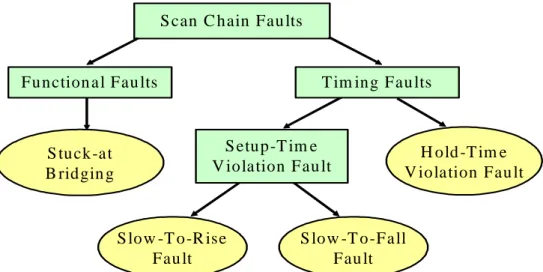
thoroughly investigated recently as in Huang [3] and, Kundu [7]. These fault types can be classified
E ach fau lt c ou ld be perm anent or interm ittent. S can C hain Fau lts
Function a l Fau lts T im ing Fau lts
S etup-T im e V iolation Fau lt S tuck-at
B ridgin g
S low -T o-R ise Fau lt
S low -T o-Fall Fau lt
H old -T im e V iolation Fau lt
Fig. 1.1: Common fault types for scan chain diagnosis
For functional faults, i.e., the logics cannot perform the desired functionality, the stuck-at
fault and the bridge fault models are mostly used. The stuck-at fault means the logic node may be
tied to power (logic 1) or ground (logic 0) via some contaminations such as particles and it causes
the node to behave the constant logic 1 or 0 (i.e. the stuck-at 1 fault model and stuck-at 0 fault model)
to violate its expected behavior. The bridge fault model is considering the un-expected connection
between two nodes, which are caused by specific sensitive layout geometry or conductive materials,
created by imperfect process such as etching. For timing faults, two types of timing violation
associated with flip-flops need to be considered: setup time violation and hold-time violation. Setup
mostly used solution is to lower down the frequency in the scan chain shifting to compensate for the
extra delay. For the latter condition, the mostly used solution is to insert some buffers to eliminate
the timing problems. For some faults, the probability of being activated is not 100%. These faults are
called intermittent faults. In general, different kinds of faults may have different faulty syndrome (i.e.
failing response) during the flush test. Thus, fault type is mostly known already when it comes to
locate the positions of failing scan flip-flops.
In the past, there are many approaches proposed to address the scan chain diagnosis problem. It
can be classified into two major categories, one is the hardware-assisted method and the other is
purely software approach. For the hardware-based methods, Schafer [12] recommend to add extra
routings from one scan chain to another, i.e. so-called partner scan chain, so the output of each scan
cell of master scan chain can connect to the partner chain for diagnosis. However if both chains are
defective, this method could fail. Edirisooriva [1] suggested to add the XOR (Exclusive-OR) at the
input of some or all scan cells, so these scan cells could flip their contents before next shifting
operation to following scan cell. Wu [15] and Narayanan [11] recommend implementing specific
scan cell design so as to flip the contents of scan cells sometime during the scan chain test. These
approaches can be performed quite efficiently with the supporting circuitry for certain types of faults
such as stuck-at faults. They may not be suitable for the hold-time violation faults, which is the main
target of this thesis.
For software methods, Kundu [7] proposed to use sequential ATPG to generate a proper test
sequence to set the flip-flops to some specific values then shift out these values for analysis.
However the sequential ATPG is more difficult than combinational ATPG, in order to overcome the
high complexity of sequential ATPG, Cheney [18] proposed to use random test patterns instead of
diagnostic patterns, using fault simulations and response matching heuristics to gauge the most likely
in the scan chain. It takes the fault-free scan chains as vehicle to set the threshold values for faulty
scan chains, so if the score is higher than the threshold values, it will be diagnosed. Thereby it
lowers down the difficulty of the diagnostic test generation process. So only combinational ATPG is
required for most cases. Guo [2] further proposed three steps for scan chain diagnosis. The 1st step is
to determine faulty chain and faulty type. The 2nd step is to identify upper and lower bounds via
some modified patterns, and the last step is using matching skills to score and rank the fault
candidates. So it can reduce the fault simulation time significantly. Huang [3,4,5] proposed the
statistical concepts to use probability for modeling the intermittent faults. Additionally the authors
also proposed an enhanced calculation to determine the upper and lower bound. Recently, Li [9][10]
further optimized the framework by incorporating the so-called single-excitation patterns and
modified ATPG techniques to provide a better scan chain diagnosis resolution. Beyond these
hardware and software assisted methods for scan chain diagnosis, there are other some techniques
used to localize the faulty flip-flop in scan chains. Hirase [8] proposed an IDDQ measurement
technique to diagnose the faulty scan chains. Song [13] proposed another point of view for scan
chain diagnosis. Since either the hardware-based or the software methods need to modify the
latch/flip-flops or require extensive data collection for post processing, the proposed technology use
the detection of light emission on the off-state leakage current to localize the faulty scan chain
problems.
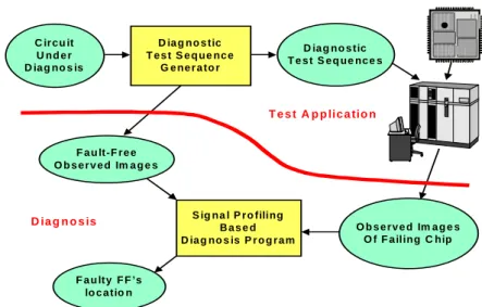
In general, the whole scan chain diagnosis flow is shown in Fig 1.2. At the first phase, generate
diagnostic test sequence to set the values of flip-flops in the scan chain (i.e. the fault-free snapshot
C ir c u it U nd e r D ia g no s is D ia g no s tic T e s t S e q ue nc e G e ne r a to r D ia g no s tic T e s t S e q ue nc e s F a u lt-F r e e O b s e r v e d Im a g e s S ig na l P r o filing B a s e d D ia g no s is P r o g r a m F a u lty F F ’s lo c a tio n O b s e r v e d Im a g e s O f F a iling C hip D ia g n o s is T e s t A p p lic a tio n
Fig. 1.2: Overall scan chain diagnosis flow.
1.1 Motives
In this thesis, we propose a new paradigm for diagnosing hold time faults in particular. The
most distinct feature of my method as opposed to previous work is that we assume less on the faulty
behavior, so we can be more robust for certain non-ideal conditions in the real world. Such as they
might have some multiple faults in a burst or the core logic may not be fault-free during the scan
chain diagnosis. The core logic may also have faults to cause the scan chain diagnosis more
challenging. Besides, the intermittent faults due to signal coupling can be dealt with in our approach
as well. In our approach, the scan chain diagnosis problem is formatted as a delay insertion
formulation. With some statistical analysis, we can isolate the locations of hold-time faults even
when the condition is not ideal such as multiple faults or a burst of faults. Since the approach
1.2 Thesis Organization
The rest of the thesis is organized as follows.
In chap 2, we present the basic diagnosis flow and also discuss two kinds of DFT test methodologies,
one is scan-capture-scan methodology which is used in current DFT test solution, another one is the
run-and-scan methodology which is used in the thesis for the diagnosis purpose.
In chap 3, we discuss the hold-time fault definitions, the fault modeling and the problem
formulation.
In chap 4, we present the principal of our greedy algorithm and also illustrate the operation of the
greedy algorithm in hold-time fault diagnosis.
In chap 5, we discuss the experimental setup and several experiment results of hold-time fault
diagnosis with greedy algorithm under ideal and non-ideal situations. It also considers the
intermittent faults problems with another experiment results.
Chapter 2
Basic Diagnosis Flow
In this chapter, we will define the necessary terminology on scan chains and the fundamental
diagnosis flow.
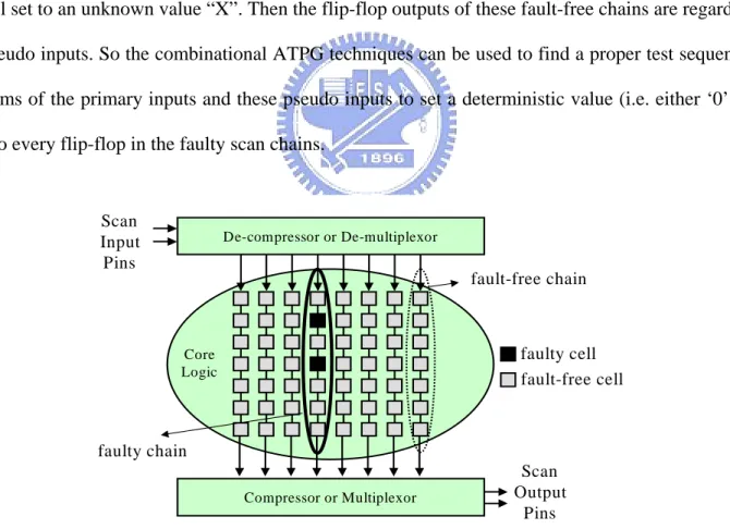
For a large design, there might be a large number of scan chains as shown in Fig 2.1. It is
common that only a small number of them can be classified as faulty scan chains after the flush test.
So one can take the advantage of these fault-free chains as the channels to diagnose the faulty one, as
proposed in Guo [2], Stanley [14]. At the beginning the flip-flop values in the identified fault chains
are all set to an unknown value “X”. Then the flip-flop outputs of these fault-free chains are regarded
as pseudo inputs. So the combinational ATPG techniques can be used to find a proper test sequence
in terms of the primary inputs and these pseudo inputs to set a deterministic value (i.e. either ‘0’ or
‘1’) to every flip-flop in the faulty scan chains.
Fig. 2.1: Architecture of scan chains.
Core Logic De-compressor or De-multiplexor Compressor or Multiplexor Scan Input Pins Scan Output Pins faulty cell fault-free cell fault-free chain faulty chain
2.1 Terminology
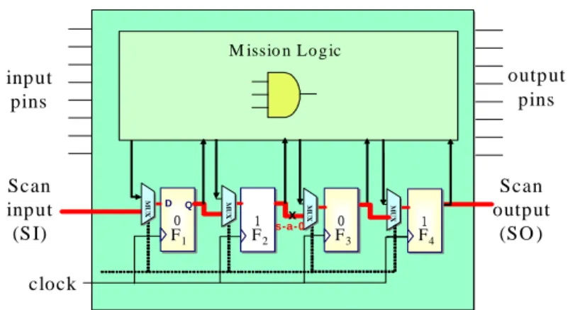
For simplicity without losing generality, we assume only one scan chain exists in the CUD (Circuit Under Diagnosis) in the thesis as shown in Fig 2.2. So there is only one scan input (SI) and
one scan output (SO), respectively. Input pins are referred to as primary inputs and output pins as
shown are referred as primary outputs. The flip-flops in the scan chain are ordered from SI to SO
sequentially, denoted as (f1, f2…, fn) assuming there are n flip-flops. The diagnosis test sequence
will be discussed in the later section.
Definition 1: (Snapshot Image) The Snapshot image of a scan chain is the value combination of the
flip-flops at certain time instance. For a fault-free circuit under diagnosis, the snapshot image is
available through the functional simulation as long as the test sequence is given. However for a
failing chip, the snapshot image of a scan chain is not available actually.
Definition 2: (Observed Image) The observed image of a scan chain is the shifted-out version of a
snapshot image. For a fault-free circuit, it is equivalent to the snapshot image. However, for a failing
chip, the bit streams collected at the scan output pin might be different from the snapshot images
fault-free. The main reason is that the presence of faults in the scan chain could distort the bit
inp ut pins clock outp ut pins Scan inp ut (S I) Scan output (SO ) M issio n Lo g ic 0 0 D Q 1 1 00 MU X MU X MU X x s-a-0 11 MU X S napshot im age : {(F1, F2, F3, F4) | (0, 1, 0, 1)} O bserved im a ge : { (F1, F2, F3, F4) | (0, 0, 0, 1)} F1 F2 F3 F4
Fig. 2.2: Snapshot image and observed image of scan chain.
Example 1: In Fig 2.2, we assume there is a stuck-at–0 fault in the scan chain path between flip-flop
2 (F2) and flip-flop 3 (F3), and the fault here will distort the bit stream propagation from scan input
to scan output. In this case, we apply some test sequence to the circuit and the mission logic will
apply the update results back to the scan chain after some combinational operation. The update
contents in these scan flip-flops are the snapshot images we defined previously, say {(F1, F2, F3, F4)
| (0,1,0,1)}. Then we shift out the contents of these flip-flops in the scan chain sequentially and get
the observed image at the scan output after 4 cycles, say {(F1, F2, F3, F4) | (0,1,0,1)}, so It is
obvious that the observed image is different from the snapshot image and It is caused by the
stuck-at-0 fault we assume in the scan chain and this fault distorts the shifted-out bit streams.
The quality of scan chain diagnosis depends on how the test patterns are applied and how the
responses are accumulated at the scan output pins. Regarding the test application, one can use either
functional patterns applied in the primary input pins or scan patterns applied to the scan input pins.
The latter one is what we call scan-capture-scan methodology and the former one is what we call
run-and-scan methodology. We will explain the two methodologies in more detail in the following
2.2 test sequence methodology
In this section, we will clarify the difference between the two test sequence generation methodologies. And for simplicity, we will also assume one stuck-at fault existing in our scan chain
to illustrate the two methods.
In Fig 2.3, we will illustrate the operation of scan-capture-scan technology and in Fig 2.4; we
will illustrate the operation of run-and-scan technology. For SCS (scan-capture-scan), It is the
typical procedure used in scan testing. Basically, it can be divided into the following steps. In step 1
as shown in Fig 2.3(a), we shift in (or scan-in) an ATPG pattern, say (1,0,1,1) in this example.
Initially, the contents of the flip-flops are unknown, so after the scan-in operation, the contents of the
flip-flop should be (1,0,1,1) from SI to SO, denoted as {f1, f2, f3, f4}. However, there is one
stuck-at-0 fault in the scan path between flip-flops f2 and f3. It distorted the contents to be (1,0,0,0)
and the down-stream part (i.e., f3 and f4) will be distorted due to the fault effect. In step 2 as shown
in Fig 2.3(b), we apply the primary input (PI) patterns, so the core combinational logic will be
executed in some way based on the distorted scan chain values, and then capture the response to
those flip-flops as (0,1,1,0). The contents of the flip-flops have been distorted once again. In Fig
2.3(c), we shift out (or scan out) the contents of those flip-flops and compare the shift-out bit stream
with expected fault-free bit stream to determine whether the scan test is passed or not. In the case,
there is a fault in the scan chain, so eventually the shift-out value will be (0, 0, 1, 0) and as we can
see, the flip-flops f1 and f2 were distorted again. So in general, the SCS (scan-capture-scan)
technology will inevitably cause two distortions during two scan-chain shifting operation (i.e.
x x x x
Combinational logic
x
1011 SA0
Fig. 2.3(a): Scan-in an ATPG pattern.
1 0 0 0
Combinational logic
x SA0
Fig. 2.3(b): Capture the response of FF’s.
0 1 1 0 Co mb in atio n al lo g ic x 0 0 1 0 S A0
the same circuit as an example to illustrate the operation of RAS. In Fig 2.4(a), after the reset, the
initial contents of these flip-flops have been determined, then we apply the functional patterns
through PI pins, and the core logic will compute accordingly and we capture the results into the
flip-flops as (0, 1, 1, 0). In step 2 as shown in Fig 2.4(b), we shift out the contents of those flip-flops,
and due to the one stuck-at fault in the scan chain, the image we observe will be (0, 0, 1, 0),
Comparing the two images and using the different profiles between the two images, we can isolate
the faulty suspicious candidates in a more efficient way.
1 1 0 S-A-0 x core logic 0
Fig. 2.4(a): Apply a test sequence at PI
S-A-0 core logic
Based on the analysis and illustration shown above, we adopt the run-and-scan method instead of
scan-capture-scan method to be our test application methodology for the scan chain diagnosis.
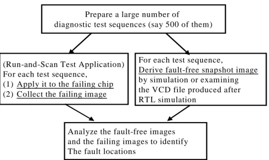
2.3 Run-And-Scan Diagnosis Flow
The diagnosis process used in the thesis is shown as Fig 2.5. Certain snapshot images are
assigned to the faulty chain first through the core logic in the functional mode before scanning out
for further analysis, as in the approach first proposed by Kundu [7].
Here, we first assume 500 diagnostic test sequences have been generated in advance. These
diagnostic sequences are derived from the test bench. Then, the fault-free images can be collected by
examining the VCD (Value Change Dump) file produced after the RTL simulation. These test
sequences are hoped to set the value of each flip-flop as random as possible, as in Cheney [18]. For
each test sequence, we apply it to the failing chip in the functional mode through primary input pins
(i.e. PI), after the core logic computation, and then scanning out the snapshot images as observed
images at the scan output pins (i.e. SO). Eventually we will have a large number of fault-free
snapshot images and failing observed images. Then we can analyze these images to produce
Fig. 2.5: Basic run-and-scan diagnosis flow.
(Run-and-Scan Test Application) For each test sequence,
(1) Apply it to the failing chip (2) Collect the failing image
For each test sequence,
Derive fault-free snapshot image by simulation or examining the VCD file produced after RTL simulation
Analyze the fault-free images and the failing images to identify The fault locations
Prepare a large number of
Chapter 3
Problem Formulation
In this section, we will first review the behavior of a hold-time violation fault and then formulate the diagnosis as a delay insertion process.
3.1 Hold-time Fault Definitions
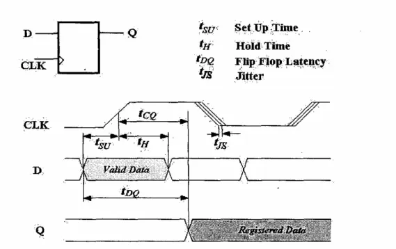
First we have the timing diagrams for a flip-flop and two flip-flops on a scan chain are shown
as Fig 3.1 and Fig 3.2 respectively (Huang [3])
Fig. 3.2 Timing diagram for a scan chain
In Fig 3.1, we observe whether the data at the input port D of the flip-flop can be propagated
and registered to its output port Q correctly. The data must be stable after the clock is active.
Otherwise the data registered at port D may be incorrect. In Fig 3.2, during the scan chain with
multiple flip-flops connected, the statement must be true to cause the hold-time error.
If tsk + tH – tCQ > td, then we will trigger the hold-time faults in which tsk is the clock skew
between clocks driving the adjacent flip-flops on the scan chain, tH is the required hold-time, tCQ is
the delay from activating clock to register the data for the driving flip-flop, and td is the propagation
delay from the output of the driving flip-flop to the input of the driven flip-flop. So why the
increase the risk to trigger the hold-time fault.
Reason 3: the propagation delay may be shorter due to the improved process technology with
high density interconnects.
3.2 Hold-time Fault modeling
Previously, Wu [15] discussed the hold-time faults and classified as three types.
Type 1: the faulty flip-flop captures the incorrect data if and only if a “0->1” transition happens at
the input of the flip-flop.
Type 2: the faulty flip-flop captures the incorrect data if and only if a “1->0” transition happens at
the input of the flip-flop.
Type 3: the hold-time fault happens whenever there is a transition at the input of the faulty flip-flop.
Besides Wu [15], Guo [2] also defined the hold-time faults as if the clock to the scan latch stays
active, then function of the faulty scan latch will behavior as a buffer that the expected value will
come out of the scan chain one cycle earlier. This hold-time fault is what the thesis target for. We
assume such hold-time fault will be triggered only in scan shift operation to have the faulty scan cell
transparent. So we refer the phenomenon that the signal at a flip-flop’s input (i.e. D-pin) changes too
fast after the clock active edge. As a result, the flip-flop can be transparent if certain clock skew
exists between driving and driven scan latch.
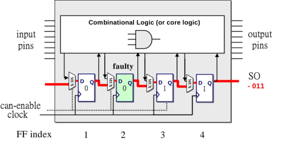
In Fig 3.4 as shown below, we use an example to illustrate the hold-time fault we are targeting
F ig. 3 .3 : T h e im p act o f a h o ld -tim e fau lt o n th e flu sh test. in pu t p in s c lo ck o u tpu t pin s C o m b in a tio n a l L o g ic (o r c o r e lo g ic ) S I S O scan -en ab le sh or t p a t h 0 0 1 1 0 0 1 1 X X X D Q D Q MU X MUX D Q MU X D Q MUX F F in d e x 1 2 3 4 fa ulty Fa u lt- fre e re sp o n se : 0 0 1 1 X X X X Fa ilin g re sp o n se : -0 0 1 1 X X X
Here we assume that the scan path between flip-flops 1 (FF index 1) to flip-flop 2(FF index 2)
is too short, thus it triggers a too-early D-pin value change during the scan chain shift operation.
Such a fault could make flip-flop2 transparent. We will say the flip-flop 2 has suffered a hold-time
fault. So from Fig 3.3, in the presence of the hold-time fault at flip-flop 2, the observed bit-stream at
the scan output (SO) pin is the same as the one we pumped into the scan chain in the flush test, but
just one cycle earlier. For example, we pumped into the scan chain with a pattern “0011” for a
fault-free chip during the flush test, then we may get the observed bit streams from the scan output
pins as “0011XXXX”. However, for a failing chip (i.e., the flip-flop 2 has a hold-time fault) with the
same pumped in pattern, we may get the observed bit streams as “ 0011XXX”. Here the “X” denotes
a don’t care bit and it depends on the rest values of the flip-flops. For the fault-free chip, we may
need to wait for 4 clock cycles to observe the pumping pattern at the scan output pin, while we only
3.3 Formulation as A Delay Insertion Process
With the run-and-scan test application methodology, we may apply a diagnostic test sequence
to the chip. After the core logic computation, the results will be captured to the flip-flops in the scan
chain, and then with scan shift operation, we can observe the snapshot images. For a failing chip, we
use the same flow to observe the snapshot images in the following two steps.
Step 1: When the diagnostic test sequence has been applied to the chip through primary input pins
(PI), but the scan shift operation is not started yet, the snapshot image will be the same as the
fault-free one. However if there is some fault in the core logic, after the core logic computation, the
fault in the logic will cause the snapshot image a slightly different from the fault-free one. The fault
effect in the core logic will be captured into the flip-flops to flip the expected contents in the scan
chains. The experiments show the difference of snapshot images caused by faulty core logic
regarded as random noise on the snapshot images.
Step 2: After the scan shift out operation, we will observe a failing image that is different from the
fault-free snapshot image by only one bit. For instance, the one bit at the faulty flip-flop is
overwritten by its preceding flip-flop due to the multi-steeping phenomenon caused by the hold-time
fault. In other words, the one bit in the snapshot image is dropped as scanned out as the final observe
image.
Example 1: Fig 3.4 shows the distortion of the hold-time fault under the run-and-scan methodology.
We assume to use a specific diagnostic test sequence determined in advance to pump into the chip to
setup the snapshot images of these flip-flops as (0011) before the scan shift out operation been
executed. Here we assume the flip-flop 2 (FF index 2) has a hold-time fault and it will be triggered
in the following scan shift out operation. During the scan shift operation, the value in the flip-flop 2
In summary, from the discussion above, we know that difference between the fault-free and
faulty snapshot images is only a number of missing bits. Therefore, we can continue to perform the
hold-time fault diagnosis by the delay insertion process to exam the image different profiles to
localize the exact failing location in the scan chain as much as possible.
Fig. 3.4 : The distortion of a hold-time fault on the image.
input pins
clock
output pins Combinational Logic (or core logic)
SO scan-enable - 011 0 0 D Q 0 0 D Q MU X MU X 1 1 D Q MU X 1 1 D Q MU X FF index 1 2 3 4 faulty
Snapshot image set up by a test sequence: (0011) Observed image: (011)
Definition 3: (Delay Insertion Process) Given a fault-free image (g1, g2…gn) and a failing observed image (f1, f2…fn) obtained with the run-and-scan methodology. The delay insertion process is to insert a number of the delayed bits “d” into the failing observed images, so the similarity of the two images could be optimized, i.e. the different bits between the two bit streams can be reduced due to the delayed bits insertions. The similarity of the two images is defined as the number of bit positions where the two images are identical. Then based on this similarity and some statistical post processing, we can localize the possible faulty flip-flops as candidates of hold-time faults.
represent the fault-free images, i.e. the snapshot images before scan shift out operation under
run-and-scan methodology and the failing images, i.e. the observed images after the scan shift out
operation which triggered the hold-time faults. Certain bits in the failing image are denoted as “-“,
meaning these values will depend on the data at the scan input pins in the second-stage of the
run-and-scan test application. From the Fig 3.5 with the simple compare manipulation, we can get
the original similarity between the fault-free image and the failing image that is calculated as 11 bits.
Now we apply the delay insertion process to insert the extra two delayed bits after the flip-flop 7 and
flip-flop 13. Then the update similarity will be calculated and increased to 16 bits. And such increase
of these similarity bits will indicate us these flip-flops we insert delayed bit may be the hold-time
fault candidates.
F i g . 3 .5 : Illu stra tio n o f d e la y in se rtio n p ro c e ss.
1 0 1 1 0 0 1 1 1 1 0 0 0 1 0 1 0 1 fa u lt-fre e im a g e fa ilin g im a g e - - 1 0 1 1 0 1 1 1 1 0 0 1 0 1 0 1 E x tra d e la y E x tra d e la y fa ilin g im a g e a fte r d e la y in se r tio n 1 0 1 1 0 d 1 1 1 1 0 0 d 1 0 1 0 1 o rig in a l s im ila rit y = 1 1 o p tim iz e d sim ila rit y = 1 6 a fte r in s e rtin g
tw o d e la ys
F F in d ex 1 2 3 4 5 6 7 8 9 1 0 1 1 1 2 1 3 1 4 1 5 1 6 1 7 1 8
d d
a fte r in s e rtin g e x tra d e la ys
Regarding the diagnosis as a delay insertion process is simply an attempt to reverse the hold-time effect. Or it can be viewed as a reconstruction method for a given distorted failing observed image to trace back the fault-free image. In the following, we will propose a Greedy algorithm to solve the hold-time diagnosis problem.
Chapter 4
Greedy Algorithm
In this section, we will explain the principal of the algorithm and illustrate the operation of the
algorithm with one example
4.1 Principal of Greedy Algorithm
The kernel of the Greedy algorithm is to insert the delay bit one by one by examining the
fault-free image and failing image simultaneously. The outline of the Greedy algorithm is shown in
Fig. 4.1. Here we use run-and-scan methodology to apply some specific diagnostic patterns to the
chip, and then with the scan shift out operation we may observe a great number of snapshot images
(say 500 images) from a fault-free scan chain, and a large number of observed images (say 500
images also) from a faulty scan chain. For each image pair, i.e. one image is from fault-free 500
images and the other one is from the 500 faulty images. We sweep them one bit at one time from the
scan output side (i.e. the flip-flop bit with the highest index) to find the proper delay candidate
position (i.e. the bit position to insert the extra delay element “d” with the delay insertion process).
When we go through the delay insertion process by checking the bits one by one, two conditions
may occur.
Condition 1: (matched case) The values of the checking bits between the fault-free and faulty images
Once the sweep is done, we will further consider the running sequence effects. Here the running
sequence means a consecutive 0’s or consecutive 1’s in the fault free image. The example as shown
in Fig 4.2 will explain the effects. In principal, if the leading bit of the running sequence is marked
as an extra delay candidate, the every rest bit in the running sequence will be marked as a delay
candidate. The heuristic is based on the observation that an extra delay inside the ant bit position in
the running sequence will lead to the identical failing image. We just can’t differentiate the more
accurate delay candidates due to the running sequence effects. In order to accommodate the
ambiguity, we take a conservative stance and regard the whole running sequence as extra delay
candidates. Once we have done the processing of one experiment with 500 image pairs, we deal with
these 500 extra delay candidates simply by summing the number of occurrences that a bit position is
marked as a extra delay candidate and rank each flip-flop position with the occurrences numbers. For
each flip-flop position, the larger the occurrences number is, the higher the rank it will be.
Fig. 4.1: The outline of a greedy algorithm.
fault-free images (say 500 of them)
failing images (say 500 of them)
Pick a pair of images (fault-free image, failing image)
Sweep the images from right (SO side) to left (SI side) Insert a delay to the failing image
immediately once a difference is found
Consider the running sequence effect
Rank the fault candidates
no more more
4.2 Operation of Greedy Algorithm
Based on the principal of greedy algorithm in previous section, we will use an example to
illustrate how the greedy algorithm work under run-and-scan methodology
Example 3: Fig 4.2 illustrates how the greedy algorithm is performed on an image pair. Similarly,
we assume the scan chain is composed of 18 flip-flops and the failing image here is caused by
hold-time faults in scan chain which is triggered under the scan shift out operation rather than the
random noise effects caused by faulty core logic computation. The first row is the flip-flop index (FF
index) starting from the scan input (i.e. SI, with the least FF index) to the scan output (i.e. SO, with
the highest FF index). Sweeping from the right to the left (i.e. from SO to SI), we found the first
difference is at bit position 11. Based on delay insertion process rule, we immediately insert one
delay element “d” at the position and move on to check the rest bits. The checking stops again at
flip-flop 5 where another extra delay element is inserted. Finally we got preliminary fault candidate
position at flip-5 and flip-flop 11. Then we consider the running sequence effect, for flip-flop 11.
The running sequence is “000” i.e. the flip-flop 11, 12 to 13. So under considering of the running
sequence effect, we also add the flip-flop 12 and 13 into our fault candidate lists. With the same
reason, we also put flip-flop 6 into our fault candidate list since the running sequence for flip-flop 5
is flip-flop 5and 6. Finally the possible hold-time fault candidates for the example will be from {FF
index 5 and 11} to {FF index 5, 6, 11, 12, 13}.
It is hard to localize the accurate hold-time fault location for greedy algorithm with one image
F ig. 4 .2 : Illu stra tio n o f a gre e d y a lgo rith m . 1 0 1 1 0 0 1 1 1 1 0 0 0 1 0 1 0 1 fau lt-free im a g e failin g im a g e - - 1 0 1 1 0 1 1 1 1 0 0 1 0 1 0 1 FF in d ex 1 2 3 4 5 6 7 8 9 1 01 1 1 2 1 3 1 4 1 5 1 6 1 7 1 8
d elay o n first d ifferen c e - 1 0 1 1 0 1 1 1 1 d 0 0 1 0 1 0 1 failin g
im a g e
d elay o n seco n d d ifferen c e 1 0 1 1 d 0 1 1 1 1 d 0 0 1 0 1 0 1 failin g im a g e co n sid er ru n n in g effect 1 0 1 1 d 0 1 1 1 1 d 0 0 1 0 1 0 1 failin g im a g e d d d d d d d ru nn in g sequ en ce d
Chapter 5
Experimental Results
In this chapter, we will depict the experimental setup first. We present the experimental results
implemented with greedy algorithm under considerations of ideal and non-ideal conditions for some
practical designs.
5.1 Experimental Setup
We have implemented the proposed approach as a system including a number of programs. The
overall experimental setup is shown at Fig 5.1. The circuit under diagnosis is given as a netlist in the
Verilog format. Then running the logic simulation to record the 5000 clock cycles snapshot images,
with the cooperation of the test sequence selection mechanism (i.e. by analyzing the logic simulation
snapshot images with the randomness criteria. We pick up a large number of test sequences to make
the signal-1 frequency of each flip-flop fall with a predefined range, say [0.3,0.7] as much as
possible to). We can get the final 500 snapshot images that have mostly random behavior per each
flip-flop in the scan chains and recorded the test sequences for the 500 snapshot images. That is the
fault-free images we may use to diagnose the hold-time faults. For failing chip, our system can inject
faults at the core logic and flip-flops in scan chains. We inject one stuck-at fault at the core logic
stem side to bring contamination for the following branches. We use the test sequence selected in
fault-free condition to apply to the fault simulator to get the corresponding 500 failing images. For
F ig . 5 .1 : E x p e r im e n ta l s e tu p . S im u l a tio n a n d T e st S e q u e n c e S e le c tio n F a u lt- fre e I m a g e s T e st be n c h T e s tbe nc h F a u lt I nje c to r a nd s im u la to r F a ilin g Im a g e s G re e d y A lg o rit hm A n a ly sis P o st-p r o c e s s ing (e .g ., s u m m in g a nd ra nk in g ) F a u lt C a n d id a te L ist in T o p 1 0 C irc u it In V e r ilo g
The experiments are performed on 4 practical designs: GCD, FIR, Montgomery Inverse and Viterbi decoder. These designs are all written in Verilog code and synthesized into their gate level netlists. The GCD is a design that computes the greatest common divisor of two given natural numbers. The FIR circuit is a digital finite impulse response filter. The Montgomery Inverse is a 32-bit integer counter. The Viterbi circuit is a channel decoder that extracts the original bit streams from the received bit streams at receive side in a communication system. The experimental setup parameters for these 4 designs are shown in Table 5.1
Table 5.1 Test circuits information and experiment setup parameters
100
500
160
11K
FIR filter
100
500
620
9.5K
Viterbi
Decoder
100
500
202
4.5K
Montgomery
Inverse
100
500
66
1.5K
GCD
Numbers of
iterations
Numbers of
functional
patterns
Numbers of
flip-flops in
scan chain
Numbers of
gate counts
Circuit Name
In general, a large design is often partitioned into a large number of scan chains to reduce the
test application time. After the flush test, the failing signatures will tell us the faulty scan chain and
the faulty behaviors. We can utilize this information to focus on a small number of scan chains that
are faulty under flush test. Then we use proper diagnosis mechanism to locate the exact faulty
flip-flops in the faulty scan chains. The 4 test cases are not the big million-gate counts design, but we
can regard these designs as a basic block that contains a complete scan chain under diagnosis. In our
experiment below, we assume only one scan chain exists in our test design cases. The basic
assumption is the flip-flops inside a small sub-design likely to be connected in the same scan chain
in the whole chip because of layout proximity. In general, a design with multiple scan chain is
consider the fault-free and faulty core logic conditions per the three experiment sets. Finally we will
also discuss the intermittent faults effects with the diagnosis
Before the experimental results, we define some terminologies used in the following summary.
These are listed below:
(1) Size: This indicates the overall gate counts in the design.
(2) Scan FF’s: This indicates the total flip-flops in the scan chain to be diagnosed.
(3) Success rate: This indicates the rate that the faulty flip-flop is included in the top 10 candidates
predicted.
(4) 1st hit index: This refers to the index of the first flip-flop in the final top 10 candidate list that
turned out to be the true faulty location. It reflects the amount of efforts a physical failure
analysis engineer needs to spend if guided by the predicted top 10 candidate lists.
(5) 2nd hit index: Similar as 1st hit index metrics, here this refers the index of the second flip-flop in
the final top 10 candidate list that turned out to be the true faulty location. For two faults or burst
fault test cases, 1st hit index means as long as one faulty flip-flop is identified in the candidate list,
it was counted as success. The 2nd hit index will count as success as long as both of the two
5.2 Single fault experiment set
In this experiment as shown in Table 5.2, we inject one single hold-time fault at scan chain
randomly for fault-free core logic and faulty core logic. We conducted 100 experiments and
calculate the average 1st hit index and the final success rate with the Greedy algorithm. The 1st hit
index is almost 1 for every design and the success rate is 100% for each design case. This implies
that it highlight the faulty location exactly for all cases we tried. The key to this success is mostly
due to the heuristic for dealing with the running sequences.
Table 5.2: Experiment results of single fault under fault-free core logic
Design Size Scan FF’s 1sthit index Success rate
GCD 1.5K 66 1.00 100% FIR 11K 160 1.00 100% Montgomery Inverse 4.5K 202 1.09 100% Viterbi decoder 9K 620 1.02 100%
For the faulty core logic, i.e. except the single hold-time fault we injected randomly, we also inject
After that, the scan shift operation will trigger the single hold-time fault we injected randomly to
have the observed images distorted. The condition is under faulty core logic; it is not an ideal
assumption that core logic is fault-free under scan chain diagnosis. From the summary in Table 5.3,
the average 1st hit index is still 1 around for GCD and FIR design. For the rest two designs, the
average 1st hit index is 2 around; it implies the Greedy algorithm still can catch the exact faulty
location in the short trial. And this will lower down the efforts for physical failure analysis engineer
to delayer the chip guided by the summary.
Table 5.3: Experiment results of single fault under faulty core logic
Design Size Scan FF’s 1sthit index Success rate
GCD 1.5K 66 1.30 91% FIR 11K 160 1.24 100% Montgomery Inverse 4.5K 202 2.19 70% Viterbi decoder 9K 620 2.21 73%
5.3 Two faults experiment set
In this experiment set, we first inject two hold-time faults randomly in the scan chain that is to
be diagnosed. Then use the same Greedy algorithm to diagnose these faulty locations. Again, we
conducted 100 experiments for each design case to derive the final average results as shown in Table
5.4. It can be seen that the results are similar to Table 5.2, which implies that under fault-free core
logic condition, the Greedy algorithm still can localize the faulty flip-flops, so it is applicable to
multiple fault situations without any modifications.
Table 5.4: Experiment results of two faults under fault-free core logic
Design Avg. 1st hit index Success rate Avg. 2nd hit index Success rate
GCD 1.00 100% 2.00 100% FIR 1.00 100% 2.00 100% Montgomery Inverse 1.03 99% 2.26 96% Viterbi decoder 1.05 100% 2.50 98%
In Table 5.5, we inject one stuck-at fault at core logic to evaluate the robustness of the proposed
average 2nd hit index, the experimental values are similar as data for major designs shown in Table
5.4, this implies the robustness of the algorithm when multiple hold-time faults exist under the faulty
core logic situation.
Table 5.5: Experiment results of two faults under faulty core logic.
Design Avg. 1st hit index Success rate Avg. 2nd hit index Success rate
GCD 1.19 90% 2.00 86% FIR 1.23 99% 2.12 97% Montgomery Inverse 1.56 68% 2.75 48% Viterbi decoder 2.32 66% 3.42 57%
5.4 Two Burst faults experiment set
In the experimental set, we apply the two hold-time faults in a burst into the scan chain at the
first time, then using the proposed approach to diagnose the observed images. The burst here means
the faulty flip-flop are connected side-by-side. The result is as shown in Table 5.6. Since the core
logic is fault-free, so the observed images that are not identical to expected snapshot images are
caused by two burst hold-time faults we injected. Again, we tested 100 times to come out the final
success rate and average hit index. The results looked pretty good for most design cases. And this
implies the algorithm not only be applicable to multiple hold-time faults but also be capable to
diagnose such multiple burst faults without further modifications.
Table 5.6: Experiment results of two burst faults under fault-free core logic
Design Avg. 1st hit index Success rate Avg. 2nd hit index Success rate
GCD 1.00 100% 2.00 100% FIR 1.00 100% 2.00 100% Montgomery Inverse 1.10 98% 2.38 97% Viterbi decoder 1.19 100% 2.60 100%
The results looked pretty nice in average hit index point of view. The performance degradation of
average hit index under faulty core logic is not so serious. The success rate for GCD, FIR design
looked well, but a little poor for the rest two design. Since we inject the stuck-at fault at stem side, so
the contamination will depend on part of circuit design to cause the success rate under faulty core
logic degrade more.
Table 5.7: Experiment results of two burst faults under faulty core logic
Design Avg. 1st hit index Success rate Avg. 2nd hit index Success rate
GCD 1.11 88% 2.13 88% FIR 1.07 98% 2.11 98% Montgomery Inverse 1.71 63% 2.85 59% Viterbi decoder 2.13 67% 3.18 60%
5.5 Intermittent faults experiment set
During the discussions in previous sections, these hold-time faults we injected are permanent
ones, i.e. these faults will exist and distort the scan chain always under the scan shift out operation.
However in real design world, many reasons will challenge the permanent faults, there may have
some process deviation, clock skew, coupling effects by high interconnect density and some specific
sensitive physical layout design geometry, so here we run the experiment to check if the proposed
Greedy algorithm can survive under the intermittent hold-time faults conditions. Likewise, we will
consider the two conditions as fault-free core logic and faulty core logic. Besides we use probability
to simulate the intermittent effects. For example, the 0.6 probability of intermittent injected
hold-time faults means we injected either single or two faults at the scan chain in advance, but the
fault we injected be triggered or not depends on the probability we defined at the beginning. We use
a random token to generate one value and compare the value with the probability we set, if the value
is less then the probability we set, the fault we injected will be triggered successfully, otherwise, it
will not be triggered during scan shift out operation under run-and-scan methodology even we inject
the faults at scan chains in advance. So for the intermittent situation, we propose several
experimental sets that cover the ideal condition (i.e. core logic is fault-free) and non-ideal condition
(i.e. core logic is faulty). Besides, per each intermittent hold-time fault, we consider the probability
Table 5.8: Experiment results of intermittent probability = 0.8, core logic is fault-free.
Single Fault Two Fault Burst Fault
Design 1st hit index Success Rate 1st hit index Success Rate 2nd hit index Success Rate 1st hit index Success Rate 2nd hit index Success Rate GCD 1.00 100% 1.00 100% 2.00 100% 1.00 100% 2.00 100% FIR 1.00 100% 1.00 100% 2.00 100% 1.00 100% 2.00 100% MON 1.07 100% 1.04 100% 2.40 96% 1.13 100% 2.25 96% Viterbi 1.19 100% 1.11 100% 2.82 98% 1.27 100% 2.70 99%
Table 5.9: Experiment results of intermittent probability = 0.6, core logic is fault-free.
Single Fault Two Fault Burst Fault
Design 1st hit index Success Rate 1st hit index Success Rate 2nd hit index Success Rate 1st hit index Success Rate 2nd hit index Success Rate GCD 1.00 100% 1.00 100% 2.00 100% 1.00 100% 2.00 100% FIR 1.00 100% 1.00 100% 2.00 100% 1.00 100% 2.00 100% MON 1.04 99% 1.03 100% 2.29 99% 1.02 99% 2.26 98% Viterbi 1.30 100% 1.19 100% 2.80 99% 1.08 100% 2.43 100%
Table 5.10: Experiment results of intermittent probability = 0.4, core logic is fault-free.
Single Fault Two Fault Burst Fault
Design 1st hit index Success Rate 1st hit index Success Rate 2nd hit index Success Rate 1st hit index Success Rate 2nd hit index Success Rate GCD 1.00 100% 1.00 100% 2.00 100% 1.00 100% 2.00 100% FIR 1.00 100% 1.00 100% 2.00 100% 1.00 100% 2.00 100% MON 1.05 100% 1.05 100% 2.49 97% 1.03 98% 2.31 96% Viterbi 1.44 100% 1.16 100% 2.75 99% 1.15 100% 2.41 99%
Table 5.11: Experiment results of intermittent probability = 0.2, core logic is fault-free.
Single Fault Two Fault Burst Fault
Design 1st hit index Success Rate 1st hit index Success Rate 2nd hit index Success Rate 1st hit index Success Rate 2nd hit index Success Rate GCD 1.00 100% 1.00 100% 2.00 100% 1.00 100% 2.00 100% FIR 1.00 100% 1.00 100% 2.00 100% 1.00 100% 2.00 100%
Table 5.12: Experiment results of intermittent probability = 0.8, core logic is faulty.
Single Fault Two Fault Burst Fault
Design 1st hit index Success Rate 1st hit index Success Rate 2nd hit index Success Rate 1st hit index Success Rate 2nd hit index Success Rate GCD 1.38 91% 1.27 90% 2.02 86% 1.06 87% 2.07 87% FIR 1.24 100% 1.17 98% 2.28 98% 1.13 98% 2.15 98% MON 2.64 78% 1.84 70% 3.08 49% 1.92 60% 2.89 54% Viterbi 2.00 70% 1.99 70% 3.46 61% 2.11 69% 2.84 61%
Table 5.13: Experiment results of intermittent probability = 0.6, core logic is faulty.
Single Fault Two Fault Burst Fault
Design 1st hit index Success Rate 1st hit index Success Rate 2nd hit index Success Rate 1st hit index Success Rate 2nd hit index Success Rate GCD 1.29 90% 1.39 93% 2.16 88% 1.24 89% 2.15 88% FIR 1.34 100% 1.32 99% 2.15 96% 1.14 97% 2.15 97% MON 1.73 66% 1.61 70% 2.94 52% 1.55 64% 2.44 59% Viterbi 2.27 70% 1.94 64% 2.98 58% 2.13 69% 3.00 64%
Table 5.14: Experiment results of intermittent probability = 0.4, core logic is faulty.
Single Fault Two Fault Burst Fault
Design 1st hit index Success Rate 1st hit index Success Rate 2nd hit index Success Rate 1st hit index Success Rate 2nd hit index Success Rate GCD 1.21 89% 1.22 90% 2.01 86% 1.27 90% 2.27 90% FIR 1.26 98% 1.53 97% 2.58 96% 1.26 97% 2.30 97% MON 2.06 68% 2.12 67% 3.52 46% 1.71 62% 2.44 55% Viterbi 2.14 64% 1.48 58% 2.87 54% 1.95 64% 2.57 58%
Table 5.15: Experiment results of intermittent probability = 0.2, core logic is faulty.
Single Fault Two Fault Burst Fault
Design 1st hit index Success Rate 1st hit index Success Rate 2nd hit index Success Rate 1st hit index Success Rate 2nd hit index Success Rate GCD 1.10 87% 1.17 89% 2.10 87% 1.01 86% 2.01 86% FIR 1.93 97% 2.34 96% 3.85 95% 1.92 96% 3.14 96%
From the intermittent experimental results shown above, it is obvious that the higher the intermittent
fault probability, the higher the diagnosis success rate .The trend is the same for each test case. And
the results meet our expectation. If we use hit index to review the diagnosis results, the 4 design
cases can have pretty good results and as we mentioned in the previous chapter that the fewer the hit
index is, the less effort the physical failure analysis needs.
In our experiments, we selected the diagnosis test sequences from the test bench. In current
VLSI design, it is common to have the multi-million gate counts. So it may partition as a large
number of scan chains in such a large design. If only few of them are faulty during the flush test, we
still can use the test generation techniques proposed by Cheney [18] and Stanley [14] in which the
fault-free scan chain are identified first during the flush test, then used as pseudo-primary inputs to
set the fault scan chains with proper desired images. In the above discussion and several
experimental results, we arrived a conclusion that the proposed Greedy algorithm can be used to
diagnose the hold-time faults in scan chains and it can have pretty nice 1st hit index under the
non-ideal condition (i.e. the core logic is faulty). Besides even the hold-time faults have a non-100%
probability to be triggered, the approach still can diagnose the hold-time faults under the intermittent
Chapter 6
Conclusion
In conclusion, when diagnosing the hold-time faults in scan chains, a number of non-ideal
situations need to be carefully considered. For example, there could be faults in core logic as well,
there could be multiple hold-time faults in the scan chain with some of them even occurring in a
burst, also there could be intermittent faults in the faulty scan chain. In this thesis, we propose a
simple yet robust greedy algorithm based on a delay insertion formulation to diagnose the hold-time
faults. We take into account the running sequence effect in the algorithm to enhance the diagnosis
resolution and achieve the robustness with non-ideal situations. Experimental results show the
algorithm is promising for the localization of the flip-flops with hold-time violation faults even
Bibliography
[1] S. Edirisooriva and G. Edirisooriva, “Diagnosis of Scan Path Failures,” Prof. of VLSI Test Symposium (VTS’95), pp. 250-255, (1995).
[2] R. Guo and S. Venkataraman, “A Technique for Fault Diagnosis of Defects in Scan Chains,” Proc. of Int’l Test Conf. (ITC’01), pp. 268-277, (2001).
[3] Y. Huang, W.-T. Cheng, S.-M. Reddy, C.-J. Hsieh, and Y.-T. Hung, “Statistical Diagnosis for Intermittent Scan Chain Hold-Time Fault,” Proc. of Int’l Test Conf. (ITC’03), pp. 319-328, (2003).
[4] Y. Huang, W.-T. Cheng, C.-J. Hsieh, H.-Y. Tseng, A. Huang, and Y.-T. Hung, “Efficient Diagnosis for Multiple Intermittent Scan Chain Hold-Time Faults”, Proc. of Asian Test Symposium, 2003.
[5] Y. Huang, W.-T. Cheng, C.-J. Hsieh, H.-Y. Tseng, Y.-T. Hung, “Intermittent Scan Chain Fault Diagnosis Based on Signal Probability Analysis”, Proc. of Design, Automation, and Test in Europe, 2004.
[6] [Jha 2002] N. K. Jha and S. K. Gupta, Testing of Digital Systems, London, United Kingdom: Cambridge University Press, 2002.
[7] S. Kundu, “ On Diagnosis of Faults in a Scan Chain,” Proc. of VLSI Test Symposium (VTS’93), pp. 303-308, (1993).
[8] J. Hirase, “Scan Chain Diagnosis Using IDDQ Current Measurement,” Proc. of Asian Test Symposium (ATS’99), pp. 153-157, (1999).
[9] J. C.-M. Li, “Diagnosis of Single Stuck-At Faults and Multiple Timing Faults in Scan Chains,” IEEE Trans. on VLSI Systems, Vol. 13, No. 6, pp. 708-718, June 2005.
[10] J. C.-M. Li, “Diagnosis of Timing Faults in Scan Chains Using Single Excitation Patterns,” IEICE Trans. on Electronics, Vol. E88-A, No. 4, pp. 1024-1030, April 2005.
[11] S. Narayanan and A. Das, “An Efficient Scheme to Diagnose Scan Chains,” Proc. of Int’l Test Conf. (ITC’97), pp.704-713, (1997).
[12] J. L. Schafer, “Partner SRLs for Improved Shift Register Diagnosis,” Proc. of VLSI Test Symposium (VTS’92), pp. 198-201, (1992).
[13] P. Song, F. Stellari, T. Xia, and A. J. Weger, “A Novel Scan Chain Diagnostics Technique Based on Light Emission from Leakage Current,” pp. 140-147, Proc. of Int’l Test Conf., 2004.
[14] K. Stanley, “High-Accuracy Flush-and-Scan Software Diagnostics,” IEEE Design and Test of Computers, pp. 56-62, (2001).
[15] Y. Wu, “Diagnosis of Scan Chain Failures,” Prof. of Int’l Symposium on Defect and Fault Tolerance in VLSI Systems (DFT’98), pp. 217-222, (1998).
[16] J.-S. Yang and S.-Y. Huang, “Quick Scan Chain Diagnosis Using Signal Profiling,” Proc. of Int’l Conf. On Computer Design, (Oct. 2005).
[17] “SIS: A system for sequential circuit synthesis,” University of California, Berkeley, Tech. Rep. M92/41, 1992.
[18] L.Cheney, N.Sheils,“ A Method for Isolating Defects in Scannable Sequential Elements”, Proc, Intel Design & Test Technology Conference, 2000.