國 立 交 通 大 學
電信工程學系
碩士論文
應用於無線區網的低溫陶瓷共燒寬頻混頻器
與低溫陶瓷共燒濾波器
LTCC Broadband Mixer and LTCC Filters for
Wireless LAN Applications
研究生:紀鈞翔
指導教授:張志揚 博士
應用於無線區網的低溫陶瓷共燒寬頻混頻器
與低溫陶瓷共燒濾波器
LTCC Broadband Mixer and LTCC Filters for
Wireless LAN Applications
研 究 生:紀鈞翔
Student:Chun-Hsiang Chi
指導教授:張志揚 博士 Advisor:Dr. Chi-Yang Chang
國立交通大學
電信工程學系
碩士論文
A Thesis
Submitted to Institute of Communication Engineering
College of Electrical Engineering and Computer Science
National Chiao Tung University
In Partial Fulfillment of the Requirements
for the Degree of
Master of Science
In
Communication Engineering
June 2004
Hsinchu, Taiwan, Republic of China
應用於無線區網的低溫陶瓷共燒寬頻混頻器與低溫
陶瓷共燒濾波器
研究生:紀鈞翔 指導教授:張志揚博士
國立交通大學電信工程研究所
摘 要
在本論文中,將呈現利用低溫陶瓷共燒技術實現寬頻混波器與三
階交錯耦合梳形濾波器及利用多層結構實現 Marchand 平衡轉換器於
無線網路 IEEE802.11a (5.2GHz, 5.7GHz) and 802.11b (2.4GHz)應用的
研發.
由於多層結構 Marchand 平衡轉換器的相速度不相等,造成輸出
端的訊號在強度與相位上更不平衡,探討 Marchand 平衡轉換器的相
速度補償且藉由補償的方式改善其效能且相當的卓著。
當實現低溫陶瓷共燒寬頻混波器時,由於螺旋型態的夾層耦合帶
線,亦會造成相速度的不相等,因此,藉由補償的方式使得混頻器更
加寬頻。
最後,設計在低於通帶端有一傳輸零點的三階交錯耦合梳形濾波
器,使得在低止帶處有較高的衰減量,並抑制所有的低頻訊號,另外,
其相當寬的上止帶與位於上止帶的零點,更能抑制二倍頻與三倍頻的
訊號。
LTCC Broadband Mixer and LTCC filters for Wireless
LAN Applications
Student:Chun-Hsiang Chi Advisor:Dr. Chi-Yang Chang
Institute of Communication Engineering
National Chiao Tung University
Abstract
This thesis presents the development of the broadband mixer and the three-pole combline filter with cross-coupling using Low temperature cofired ceramics (LTCC) technology and the Marchand balun using the multilayer structure for IEEE802.11a (5.2GHz, 5.7GHz) and 802.11b (2.4GHz) wireless LAN applications.
The difference in phase velocity of the Marchand balun in multilayer structure makes the amplitude and phase more unbalanced at output ports. Compensating the difference in phase velocity of the Marchand balun is studied and it can improve the performance of the Marchand balun significantly.
When implementing LTCC broadband mixer, the difference in phase velocity also can be found due to the spiral broadside coupled stripline. Therefore, compensation in phase velocity increases the bandwidth of the mixer.
Finally, the design of the three-pole combline filter with cross-coupling with the characteristic of having transmission zeros at the low-side skirt can generate a high attenuation rate and suppress all the lower stopband signals. Beside, the filter with broad stopband and transmission zeros at the high-side skirt can suppress the second harmonic and third harmonic.
Acknowledgment
誌謝
能夠完成此論文,首先,要感謝指導教授張志揚博士在這兩年求學生 涯中,給予指導與鼓勵,不僅讓我在微波領域知識獲益良多,也在研究方 式與態度有所增長。同時也要感謝口試委員楊正任博士、邱煥凱博士及周 復芳博士的不吝指導,使得此篇論文更為完善。另外,也要感謝謝華新科 技全力協助完成 LTCC 電路的製作。 感謝實驗室的學長及同窗好友牧榮、澤民、俊毅、湘竹和實驗室的學 弟妹們,讓實驗室不再是刻板印象中毫無生氣的實驗室,而是充滿生機的 實驗室,使我的研究生活添加不少的樂趣。當然,最後要感謝陪我一路走 來的家人,你們毫無保留的付出,讓我無後顧之憂地生活與求學,給我最 大的支持與鼓勵,我能有現今的一切,都是你們的功勞。 最後,將此論文獻給我最愛的父親以及母親。Contents
Abstract (Chinese)………I Abstract ...…………...………...II Acknowledgments………Ⅲ Contents………Ⅳ List of Tables……..………...………...……Ⅵ List of Figures……….….…………...……….Ⅶ Chapter 1 Introduction……….….….1Chapter 2 Compensated Marchand balun………..………….…...5
2.1 Analysis of the Marchand balun….…………..………...…6
2.2 Realization of the Marchand balun.…....……….…9
2.3 Realization of the compensated Marchand balun with a short transmission line….………..….13
2.4 Fabrication of the modified Marchand balun………....…...20
Chapter 3 The Broadband LTCC Doubly Balanced Mixer……..……….……..…….23
3.1 The property of the Schottky diode ………...…….…………...….23
3.2 Analysis of double-balanced ring mixer………..…………...…25
3.3 Realization of the Broadband LTCC double-balanced mixer………..….…...27
3.4 Simulated results of the double-balanced mixer………...…...…..35
Chapter 4 Comb-line filter with capacitive cross-coupling………..……..….38
4.1 Theory of the combline filter..………...……….…..….38
4.2 Phase relationships………..………...41
4.3 Design of the LTCC three-poles combline filter with cross-coupled capacitor……….………..………43
5.1 Substrate effect……….……….……….51
5.2 Shielding box effect………..………..………...55
Chapter 6 Conclusion……….………..57
List of Tables
Table 1.1 Specifications of the filters for wireless LAN………...………...3 Table 3.1 Dimension comparison between BCS and SBCS………29 Table 4.2 Total phase shifts for two paths in a CT section with capacitive
cross-coupling………..43 Table 5.1 Various box sizes vs. the locations of transmission zeros………....56
List of Figures
Figure 1-1 LTCC balanced diplexer module for wireless LAN applications……….…2 Figure 2.1-1 Marchand balun (a) Coaxial cross section (b) Equivalent transmission line model……….………..6 Figure 2.1-2 Basic logic of the Marchand balun………..….….…7 Figure 2.1-3 Schematic of the symmetrical Marchand balun as two identical……..…8 Figure 2.2-1 Realization of the Marchand balun (a) top view of the Marchand balun (b) side view……….……10 Figure 2.2-2 (a) Equivalent circuit in this design (b) Return loss of the transmission line model in (a)…………...………...…..11 Figure 2.2-3 Simulated results of the Marchand balun…..………..………...….12 Figure 2.2-4 Simulated results of the amplitude unbalance and the phase unbalance.12 Figure 2.3-1 Even mode and odd mode transmission phase vs. frequency…..……....14 Figure 2.3-2 Circuit diagram of proposed topology…….….………...……14 Figure 2.3-3 Top view of the compensated Marchand balun with the short
transmission line………...………..……..…15 Figure 2.3-4 3-D structure of the proposed Marchand balun...…………..…..………15 Figure 2.3-5 Operational bandwidth of the compensated Marchand balun………….16 Figure 2.3-6 Amplitude unbalance with various transmission line impedances……..17 Figure 2.3-7 Phase unbalance with various transmission line impedances…………..17 Figure 2.3-8 Simulated responses of the Marchand balun………..…………..……...18 Figure 2.3-9 Simulated phase responses of the Marchand balun………...18 Figure 2.3-10 Simulation results of the amplitude unbalance and the phase
Figure 2.3-11 Simulated results of the amplitude unbalance and the phase unbalance for compensated and uncompensated Marchand balun..………..……19 Figure 2.4-1 Photograph of fabricated balun………...………….20 Figure 2.4-2 Measured responses of the Marchand balun………21 Figure 2.4-3 Measured phase responses of the Marchand balun…….……..………..21 Figure 2.4-4 Measured results of the amplitude unbalance and the phase unbalance..22 Figure 3.1-1 Equivalent circuit and I-V curve of a diode (a) The equivalent circuit of the diode (b) I-V curve of the diode………..……...……...24 Figure 3.1-2 Current and conductance waveform of the diode (a) Current waveform
(b) Conductance waveform……….………..……..24 Figure 3.2-1 Analysis of double-balanced ring mixer………..………25 Figure 3.2-2 Voltage and current waveform of the diodes (a)LO voltage and current (index:n) (b) RF voltage and current (index:m)…….…….……..……...25 Figure 3.3-1 Lump element equivalent circuit of the symmetrical coupler…….…....28 Figure 3.3-2 LTCC Marchand balun (a) Top view of the LTCC Marchand balun
(b) Side view of the Marchand balun………...……29 Figure 3.3-3 3D structure of the LTCC Marchand balun…………..………..……….30 Figure 3.3-4 Simulated results of the Marchand balun……….……..…….31 Figure 3.3-5 Simulated results of the amplitude unbalance and the phase unbalance.32 Figure 3.3-6 Schematic of the Marchand balun with IF output……….…….….……32 Figure 3.3-7 Simulated results of the Marchand balun……….…..…….33 Figure 3.3-8 Simulated results of the amplitude unbalance and the phase unbalance.33 Figure 3.3-9 3D structure of the double-balanced mixer……….………....34 Figure3.4-1 Conversion loss vs. RF frequency for RF balun center tap……….…...35 Figure3.4-2 Conversion loss vs. RF frequency for LO balun center tap……….…...35
Figure3.4-3 LO-IF, LO-RF, RF-IF isolation vs. RF frequency for RF balun center
tap……….36
Figure3.4-4 LO-IF, LO-RF, RF-IF isolation vs. RF frequency for LO balun center tap………...………....……..36
Figure3.4-5 Conversion loss vs. IF frequency for RF balun center tap.…………..…37
Figure 4.1-1 Typical combline bandpass filter………..………...39
Figure 4.1-2 Transformation of equivalent circuit of coupled line………...39
Figure 4.1-3 Schematic of J-inverter……….……...39
Figure 4.1-4 Equivalent circuit of the combline filter………..40
Figure 4.1-5 J inverter equivalent circuit for the combline filter……….…40
Figure 4.1-6 Lump element equivalent circuits of the combline filter………….……40
Figure 4.2-1 Phase shifts for series capacitor, series inductor and shunt inductor/capacitor pairs (a) Series capacitor, (b) Series inductor, (c) Shunt inductor/capacitor pairs………42
Figure 4.2-2 CT section (a) Multi-path coupling diagram for CT section with capacitive cross-coupling (b) Possible frequency response……….……43
Figure 4.3-1 Modified combline filter……….………44
Figure 4.3-2 Equivalent circuit of the modified combline filter………...…....……...44
Figure 4.3-3 Simulated responses of the combline filter with Microwave Office…...45
Figure 4.3-4 Applying Y-parameter to analyze the transmission zeros.……….….….46
Figure 4.3-5 Combline filter and cross-coupled capacitor……….…………..46
Figure 4.3-6 3-D structure of the LTCC combline filter………...………...…47
Figure 4.3-7 EM simulated results of the LTCC combline filter……….………48
Figure 4.3-8 Modified combline filter with the inductance L……….…...…..48
Figure 4.3-9 Simulated responses of the combline filter with Microwave Office…...49
Figure 4.3-11 Comparison of measured results and EM simulated results (GSG
probe)………..……….50
Figure 4.3-12 Photograph of the LTCC combline filter………...50
Figure 5.1-1 Overall schematic of the LTCC filter………...………...51
Figure 5.1-2 Measured environment with substrates………...………52
Figure 5.1-3 EM simulated results for substrate environments………52
Figure 5.1-4 EM simulated responses for GSG probe and substrate environments….53 Figure 5.1-5 EM simulated results with various via-holes………...………53
Figure 5.1-6 Comparison of measured results and EM simulated results………54
Figure 5.1-7 Photograph of the LTCC combline filter……….55
Figure 5.2-1 EM simulation result with various box sizes……….…..56
Chapter 1 Introduction
In recent years, the wireless communication market has experienced explosive growth. There is increasing demand to make portable communication systems lighter, more compact, and better functionality. The ceramic multilayer substrate technology such as LTCC (Low temperature cofired ceramics) enables the creation of monolithic, three-dimensional, cost-effective microwave circuits and modules [1-5]. Monolithic LTCC structures incorporating buried components and surface-mounted components allow increased design flexibility by providing a mechanism for establishing microstrip, stripline, coplanar waveguide and DC lines within the same medium. Additionally, the reduced weight of LTCC packages and the low loss characteristics of the dielectric and conductors make LTCC an ideal candidate for high performance commercial and military electronic systems. Integrated passive components such as filters, couplers, baluns and impedance transformers are usually based on transmission line sections of quarter wavelengths. Hence, the sizes of these circuits are large at low frequencies.
Today’s wireless telecommunication for dual-band applications such as IEEE802.11a (5.2GHz, 5.7GHz) and 802.11b (2.4GHz) wireless LAN have increased rapidly. The broadband characteristic of the balun has the potential to provide various wide-band applications such as broadband mixer [6-14]. Recently, monolithic Marchand baluns have been revisited and shown to be feasible in wireless communication applications. However, they suffer from high amplitude and phase unbalance at output ports.
Figure 1-1 shows the balanced diplexer module that will be implemented and integrated by LTCC technology for wireless local area network (LAN) applications.
The diplexer module will meet the specifications of IEEE 802.11a(5.2GHz、5.7GHz) and 802.11b(2.4GHz) wireless LAN. In the wireless LAN applications, the image signal needs to be highly attenuated to maintain the high quality signal received from the antenna. Moreover, the leakages of harmonics from the transmitted circuit appearing in the received circuit must be suppressed. Using the technique of cross-coupling to produce transmission zeros, the rejection below the passband is increased. This can reduce the number of resonating elements required to meet a specification and this, in turn, reduces the insertion loss, size, manufacturing cost of the design and tuning time. Therefore, the filter with the characteristic of having transmission zeros at the low-side skirt can generate a high attenuation rate and suppress all the lower stopband signals. The filter with broad stopband and transmission zeros at the high-side skirt can suppress the second harmonic and third harmonic.
The SIR (Stepped Impedance Resonators) filter [15] and combline filter [3, 16-20] have the characteristic of broad stopband due to the destruction of the periods of resonators. However, the combline filter has more compact size than the SIR filter. Therefore, it has been widely used in wireless communication systems.
SW Rx:5 GHz BPF BPF LPF LPF diplexer diplexer BPF BPF BLN BLN Hz Rx:2.4 G Tx:2.4 GHz 2.4/5 GHz 2.4&5GHz 2.4 & 5GHz Tx:5 GHz
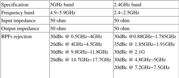
Specification 5GHz band 2.4GHz band Frequency band 4.9~5.9GHz 2.4~2.5GHz Input impedance 50 ohm 50 ohm Output impedance 50 ohm 50 ohm BPFs rejection 30dBc @ 0.5GHz~4GHz 20dBc @ 4GHz~4.5GHz 30dBc @ 9.8GHz~11.8GHz 20dBc @ 14.7GHz~17.7GHz 30dBc @0.88GHz~1.785GHz 35dBc @ 1.85GHz~1.91GHz 30dBc @ 2.1G 30dBc @ 4.8GHz~5GHz 20dBc @ 7.2GHz~7.5GHz Table 1.1 Specifications of the filters for wireless LAN
In Chapter 2, the Marchand balun has been implemented by two substrates. However, it suffers from high amplitude and phase unbalance at output ports. Adding a short transmission line between two microstrip broadside coupler to compensate the difference between even mode and odd mode phase velocity is proposed.
In Chapter 3, we will develop the broadband double-balanced mixer with LTCC technology. The ceramic substrate of the LTCC has dielectric constant of 7.8. To achieve broad bandwidth in designing the double-balanced mixer, broadband baluns are the key components in the mixer. In this design, using spiral broadside coupled stripline to implement the Marchand balun has more compact size. However, the same phenomenon can be found in the spiral broadside coupled stripline discussed in Chapter 2. Therefore, we also compensated the even and odd mode phase velocities with a transmission line.
In Chapter 4, the three-pole combline filter with cross-coupling is proposed. Table 1.1 shows the specifications of the filter in Figure 1-1. The LTCC dielectric constant is 33 and each layer thickness is 1.2mil. Therefore, we can minimize the circuit as small as possible.
In Chapter 5, the substrate and the shielding box effects for the three-pole combline filter with cross-coupling are discussed.
Chapter 2
Compensated Marchand balun
Baluns are key components in balanced circuit topologies such as double- balanced mixers, push-pull amplifiers, frequency doublers, antenna feed networks and phase shifters. The word balun is an acronym for balanced-to-unbalanced converter, and the function is employed to change an unbalanced signal to a balanced signal with equal potential but opposite polarity. The four-port passive circuits, such as rat-race hybrids and waveguide magic tees, can be used as baluns. Major limitations of these components are their narrow bandwidths and the lack of a method for center-tap grounding. Most coupled lines based baluns require a high even mode to odd mode impedances ratio, one order of magnitude or more. This results in good balance and reasonable bandwidth. The Marchand balun has a better bandwidth and more balanced outputs than the coupled line baluns because the smaller difference between the even and odd mode impedance compared with what is needed for the coupled line balun case. Proper selection of balun parameters can achieve a bandwidth of more than 10:1.
The Marchand balun is perhaps one of the most attractive due to its planar structure and wide-band performance [6-7]. Beside, multilayer configurations make MIC/MMIC more compact and can exhibit wide bandwidths due to tight coupling in coupled line baluns [8-14].
2.1 Analysis of the Marchand balun
The Marchand balun is a derivative of one of the first balun configurations that was physically realized in a coaxial configuration as shown in Figure 2.1-1(a). The equivalent transmission line model for the Marchand balun is shown in Figure 2.1-1(b). = 900 at fo
Z
0Z
S1 θ θZ
S2Z
BZ
1Z
R
L (a)Z
BZ
S2Z
S1Z
1Z
2Z
0Z
L (b)Figure 2.1-1 Marchand balun (a) Coaxial cross section
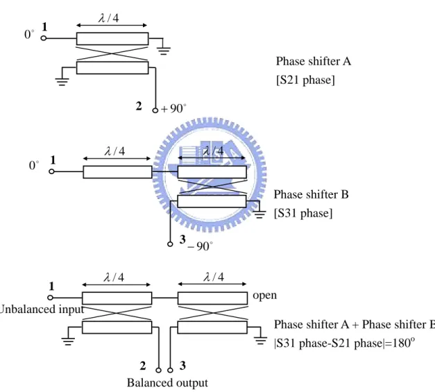
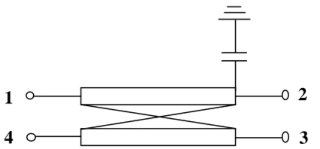
The Marchand balun basically consists of an unbalanced, an open-circuited, two short circuited, and balanced transmission line sections as shown in figure 2.1-2. Each section is about a quarter-wavelength long at the center frequency of operation. The Marchand balun consists of two coupled sections, which may be realized using microstrip-coupled lines, Lange couplers, multilayer coupled structures, or spiral coils. 4 / λ o 90 + 2 1 o 0 Phase shifter A [S21 phase] 4 / λ o 90 3 − 1 λ/4 o 0 Phase shifter B [S31 phase] 4 / λ open 3 2 1 Unbalanced input 4 / λ
Phase shifter A + Phase shifter B |S31 phase-S21 phase|=180o Balanced output
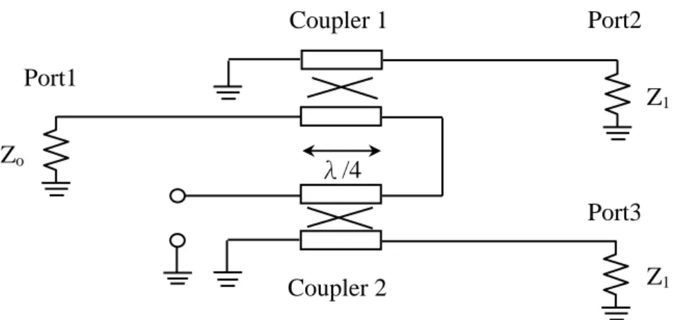
Port2 Coupler 1 Coupler 2 Zo Z1 Z1 Port1 Port3 λ/4
Figure 2.1-3 Schematic of the symmetrical Marchand balun as two identical Figure 2.1-3 shows the schematic of the Marchand balun as two identical couplers. For symmetrical baluns, the scattering matrix of the balun can be derived from the scattering matrix of two identical couplers. The unbalanced input impedance is Zo and the balanced output impedance is Z1. If the source impedance and load
impedances are equal to Zo, the scattering matrix for ideal couplers with infinite
directivity and coupling factor C is given by
(2.1)
[ ]
2 2 2 20 -
1-
0
0 0 -
-
1-
0 0
0 -
1-
coupler
C
j
C
C
j
C
S
j
C
C
j
C
=
0
C
⎡
⎤
⎢
⎥
⎢
⎥
⎢
⎥
⎢
⎥
⎢
⎥
⎢
⎥
⎣
⎦
[ ] ⎥ ⎥ ⎥ ⎥ ⎥ ⎥ ⎥ ⎥ ⎥ ⎥ ⎥ ⎥ ⎥ ⎥ ⎥ ⎥ ⎥ ⎦ ⎤ ⎢ ⎢ ⎢ ⎢ ⎢ ⎢ ⎢ ⎢ ⎢ ⎢ ⎢ ⎢ ⎢ ⎢ ⎢ ⎢ ⎢ ⎣ ⎡ ⎟⎟ ⎠ ⎞ ⎜⎜ ⎝ ⎛ − + − ⎟⎟ ⎠ ⎞ ⎜⎜ ⎝ ⎛ − + ⎟⎟ ⎠ ⎞ ⎜⎜ ⎝ ⎛ − + − − ⎟⎟ ⎠ ⎞ ⎜⎜ ⎝ ⎛ − + ⎟⎟ ⎠ ⎞ ⎜⎜ ⎝ ⎛ − + − ⎟⎟ ⎠ ⎞ ⎜⎜ ⎝ ⎛ − + − ⎟⎟ ⎠ ⎞ ⎜⎜ ⎝ ⎛ − + − − ⎟⎟ ⎠ ⎞ ⎜⎜ ⎝ ⎛ − + − ⎟⎟ ⎠ ⎞ ⎜⎜ ⎝ ⎛ − + ⎟⎟ ⎠ ⎞ ⎜⎜ ⎝ ⎛ + − = 1 2 1 1 1 2 1 2 1 2 1 1 2 1 2 1 2 1 2 1 1 1 2 1 1 2 1 2 1 1 2 1 2 1 1 2 1 2 1 1 2 1 0 1 2 2 0 1 2 0 1 0 1 2 0 1 2 0 1 2 0 1 2 0 1 2 2 0 1 2 0 1 2 0 1 2 0 1 2 0 1 2 0 1 2 0 1 2 0 1 2 Z Z C C Z Z C Z Z C j Z Z C Z Z C C j Z Z C Z Z C j Z Z C C Z Z C Z Z C C j Z Z C Z Z C C j Z Z C Z Z C C j Z Z C Z Z C Sbalun (2.2)
Equation (2.2) shows that the use of identical coupled sections results in balun outputs of equal amplitude and opposite phase, regardless of the coupling factor and port terminations. To achieve optimum power transfer of –3dB to balanced port, we require (2.3) 2 / 1 31 21 = S = S
With (2.2) and (2.3), the required coupling factor for optimum balun performance is give by 1 2 1 1 + = o Z Z C (2.4)
With equation (2.4), we can design the Marchand balun by determining one of two variables and the other can be obtained. If we choose all the ports are terminated with 50Ω, the required coupling factor is –4.8dB. Then, the coupled line will be designed to meet the required coupling factor.
2.2 Realization of the Marchand balun
To increase the even mode and odd mode impedance ratio, we implemented the Marchand balun with microstrip broadside couplers. The Marchand balun was
fabricated using Rogers 4003(εr=3.38) with multilayer structures. The substrate consists of 2 layers, the lower layer of 20mil and the upper layer of 8mil as shown in Figure 2.2-1(b). Figure 2.2-1 shows the side view and the top view of the implemented Marchand balun. The dimensions for the various line sections are input line A has a 16 mil line-width and is 447 mil long. The line width, length for the open-circuited line B and short-circuited lines C are 24 mil, 447 mil and 30 mil, 447 mil, respectively. The unbalanced input impedance is 50Ω and the balanced output impedance is 50Ω. A B C C Via Via Balanced output Unbalanced input
Top
Bottom metal
(a) Ground plane 38 . 3 = r ε 38 . 3 = r ε 8mil 20milFigure 2.2-1 Realization of the Marchand balun (a) top view of the Marchand balun (b) side view
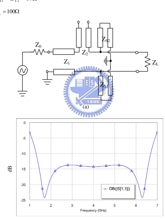
Figure 2.2-2(a) shows the equivalent transmission line model of the Marchand balun in Figure 2.2-1(a). Corresponding values of the transmission line model are:
Ω = 50 Zo Ω = 58.18 1 Z Ω = 42.7 2 Z Ω = = 2 64 1 S S Z Z Ω = 100 L Z
Z
S2Z
S1Z
1Z
2Z
0Z
L (a) dB (b)Figure 2.2-2(a) Equivalent circuit in this design (b) Return loss of the transmission line model in (a)
dB
Figure 2.2-3 Simulated results of the Marchand balun
Am p litud e u nbalance (dB ) Phase unbalance (de g ree )
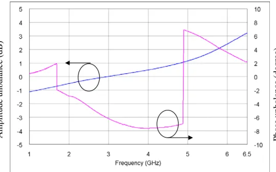
Figure 2.2-4 Simulated results of the amplitude unbalance and the phase unbalance The balun has been simulated on a full-wave EM simulator (Sonnet). Figure 2.2-3 and Figure 2.2-4 show the amplitude unbalance at balanced output ports is within 1dB,and the phase unbalance at balanced output ports is less than over the frequency range of 1.6 to 4.8GHz where |S
o
10
2.3 Realization of the compensated Marchand balun with a short transmission- line From the simulated results in Figure 2.2-3 and Figure 2.2-4, the phase and amplitude balance of the Marchand balun are poor. The main reason for the poor balance is the difference between even mode and odd mode phase velocity (Stringently speaking, the normal mode of the broadside microstrip coupler are c mode and π mode). However, the results of the even and odd mode excited method meet the coupling of the couplers. Beside, several papers [2,8] also simplify c mode and π mode as even mode and odd mode. Therefore, we explain the mechanism of the Marchand balun with even and odd mode. The coupled electrical length θ, even mode transmission phase θe and odd mode transmission phase θo are given by
2 / ) (θe θo θ = + (2.5) (2.6) e p e ωL/V θ = (2.7) o p o ωL/V θ =
where ω is the operation frequency, L is the physical length of coupled line, and are the even mode and odd mode phase velocities, respectively. For the microstrip broadside structure, because the even mode phase velocity is always faster than odd mode phase velocity,
e p
V Vpo
o
θ is always larger than θe for all frequencies as shown in Figure 2.3-1. Therefore, the difference between the even mode and odd mode phase velocity degrades the bandwidth of the Marchand balun.
Compensation for the difference in normal mode phase velocity in the broadside-coupled structure is required. Adding capacitors at four ends of the couplers in [2] is effective in improving the difference between the even mode and odd mode phase velocity. But it needs too many capacitors for compensation. Therefore, compensation is accomplished by connecting a short transmission line to a pair of couplers. The short transmission line acts like placing the capacitor to ground (see
Figure 2.3-2), instead of between the plates, would have the effect of “slowing down” the even mode phase velocity. As shown in Figure 2.3-1, the dot lines are the transmission phases of the even mode and odd mode in the uncompensated coupler and the solid lines are the transmission phases of the even mode and odd mode in the compensated coupler. Adding the capacitor in one end is effectively in improving the difference between the even mode and odd mode phase velocity.
T ransmissio n p hase (De g ree )
Figure 2.3-1 Even mode and odd mode transmission phase vs. frequency
2 1
4 3
Figure 2.3-2 Circuit diagram of proposed topology
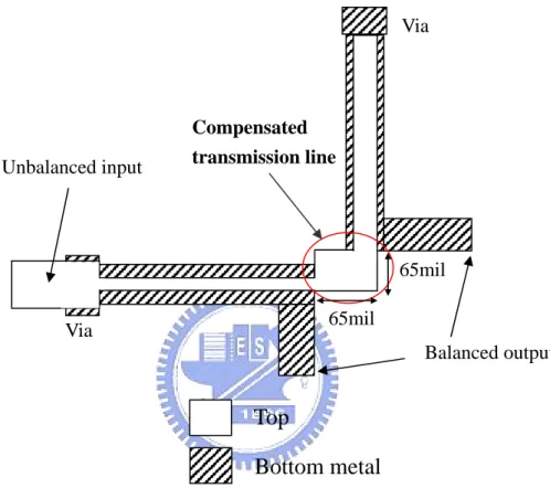
transmission line between two couplers. The dimensions of the modified Marchand balun and the Marchand balun in Figure 2.2-1 are the same except the middle transmission line. Figure 2.3-4 shows the proposed 3-D structure of the Marchand balun. Via Via 65mil 65mil Balanced output Unbalanced input Compensated transmission line
Top
Bottom metal
Figure 2.3-3 Top view of the compensated Marchand balun with a short transmission line
0.8 0.9 1 1.1 1.2 40 45 50 55 60 65 70 75 80
transmission line impedanc
Normalized bandwidth e 65mil zo 3 2 1 ∆f /fo zo ) (Ω
Figure 2.3-5 Operational bandwidth of the compensated Marchand balun.
Figure2.3-5 indicates the operational frequency of the compensated Marchand balun as a function of transmission line impedance. The bandwidth is defined as the frequency range yielding the amplitude difference within 1dB, the phase unbalance within10o and |S11|< -10dB. These difference result in more than 20-dB suppression
of the undesired signal when the balun is in balanced mixers. The bandwidth increases when Zo decrease and is maximum at line impedances from 58 to 46 Ω for the line
length of 65mil. Lower line impedances degrade the bandwidth because the amplitude and phase differences caused by the added transmission line are too large to compensate for the differences of the Marchand balun.
Z=71 Z=62 Am p litud e u nbalance (dB ) Z=55 Z=50 Z=46 Z=42
Figure 2.3-6 Amplitude unbalance with various transmission line impedances
Phase unbalance (de g ree ) Z=71 Z=62 Z=55 Z=50 Z=46 Z=42
Figure 2.3-7 Phase unbalance with various transmission line impedances
Figure 2.3-6 and Figure 2.3-7 show that the amplitude unbalance and phase unbalance with various transmission line impedances. Although the amplitude unbalance is within 1dB and phase unbalance is less than 5o over the frequency range of 1.6 to 6.21Hz at the line impedances from 58 to 46 Ω, the optimum line impedance
can obtained from Figure 2.3-6 and Figure 2.3-7. The optimum line impedance is about 50Ω for the line length of 65mil. Therefore, we choose the short transmission line (65 mil×65 mil) as our design between two couplers. The simulated responses of the modified Marchand balun are shown in Figure 2.3-8, Figure 2.3-9 and Figure 2.3-10.
dB
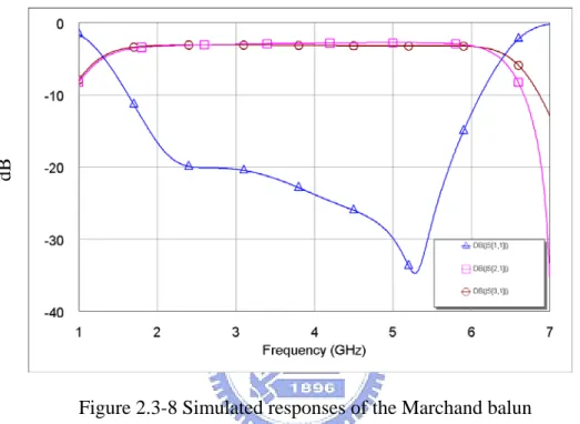
Figure 2.3-8 Simulated responses of the Marchand balun
De
g
ree
Am p litud e u nbalance (dB )
Phase unbalance (degree)
Figure 2.3-10 Simulated results of the amplitude unbalance and the phase unbalance
Am p litud e u nbalance (dB )
Phase unbalance (degree)
Figure 2.3-11 Simulated results of the amplitude unbalance and the phase unbalance for compensated and uncompensated Marchand balun
From the simulated results shown in Figure 2.3-8, the S11 is less than –10dB in
the range of 1.6 to 6.1GHz. The differences of the amplitude and phase between the balanced output ports are shown in Figure 2.3-10. The amplitude unbalance at
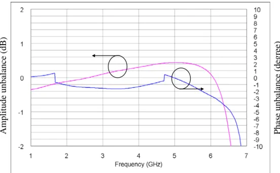
balanced output ports is within 0.5 dB, and the phase unbalance at balanced output ports is less than 3o over the frequency range of 1.6 to 6.1GHz where |S11|< -10dB.
Figure 2.3-11 shows the noticeable improvement in the amplitude balance and phase balance for the Marchand balun with the optimum compensated transmission line.
2.4 Fabrication of the modified Marchand balun
Figure 2.4-1 shows the photograph of the fabricated balun. We add the short transmission line (65 mil×65 mil) between two couplers. To implement the two-layer configuration, we use the plastics screws that have seldom effects to the circuit to fix the two substrates.
Plastics screws
dB
Figure 2.4-2 Measured responses of the Marchand balun
De
g
ree
Phase unbalance (degree) Am p litud e u nbalance (dB )
Figure 2.4-4 Measured results of the amplitude unbalance and the phase unbalance
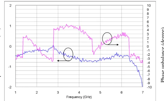
From the measured results shown in Figure 2.4-2, the S11 is less than –10dB in the
range of 1.9 to 6.2GHz. The differences of the amplitude and phase between the balanced output ports are shown in Figure 2.4-4. The amplitude unbalance at balanced output ports is within 1dB, and the phase unbalance at balanced output ports is less than 5o over the frequency range of 1.6 to 6.2 GHz where |S11|< -10dB. In Figure
2.3-9 and Figure 2.4-3, the output signals of measured phase responses have more periods than simulated phase responses. This is because the output transmission lines and the SMA connectors are neglected in EM simulation. These neglected components contribute the electrical length for output signals. Hence, the fabricated balun has more periods.
Chapter 3
Broadband LTCC Doubly Balanced Mixer
Figure3.2-1 shows a double-balanced ring mixer. It consists of two transformers and a ring of identical diodes. The advantages over the double-balanced mixer are inherent isolation between all port, rejection of LO noise and spurious signals, rejection of spurious responses and certain intermodulation products, and extremely broadband operation. The disadvantages are the need for four diodes and two hybrids, greater LO power requirements, and generally higher conversion loss than single-diode or singly balanced mixers.
3.1 The property of the Schottky diode
The Schottky diode is a non-linear device. The equivalent circuit and I-V curve can be expressed in Figure 3.1-1. It consists of capacitor C(v), resistor R(v) as a function of the voltage and a fixed series resistor Rs. The non-linear characteristic of R(v) is used in designing mixer. When pumping the Schottky diode with greater local oscillator (LO) power, the signal would be rectified (only the positive cycle can turn on the diode). Hence, the diode current iLO(t) and conductance waveform gLO(t) is
shown as Figure 3.1-2. The Fourier series expansion of gLO(t) can be expressed as
following.
∑
∞ ∞ = = -n n n LO(t) g g ej wLOt (3.1) Because the non-linear characteristic of the diode, the diode involves harmonics of RF frequency when RF signal is applied to the diode at the same time. The Fourierseries expansion of the RF voltage can be given by
∑
∞ ∞ = = -m t w m j m RF RF e V (t) V (3.2)Hence, the current id on the diode produced by VRF and gLO can be expressed as
following.
∑ ∑
∞ ∞ = ∞ ∞ = + = -m n -t ) nw w m ( j m n d LO RF e V g (t) i (3.3)The diode current id involves all intermodulation products of the RF frequency
and LO frequency. The terms which (m,n) equals (1,-1) or (-1,1) are the desired signals(IF signals). The low pass filter can eliminate all other higher order terms.
Rs R(v) V Nonlinear area I C(v)
(a) The equivalent circuit of the diode (b) I-V curve of the diode Figure 3.1-1 Equivalent circuit and I-V curve of a diode
t LO f 1 = τ i(t) 0 0 t g(t) (b) Conductance waveform (a) Current waveform
3.2 Analysis of double-balanced ring mixer RF virtual ground id2 id1 id4 LO virtual ground A’ RF virtual ground id3 iif1 iif2 RF balun RF IF B’ B LO balun A LO virtual ground. LO
Figure 3.2-1 Analysis of double-balanced ring mixer
Vd1 τ 2 id2 2 τ id4 id3 id1 Vd1 τ 2 id2 2 τ id4 id3 id1 Vd2 Vd2 Vd3 Vd3 Vd4 Vd4 (b) (a)
Figure 3.2-2 Voltage and current waveform of the diodes (a) LO voltage and current (index:n) (b) RF voltage and current (index:m)
The RF signal is applied to the primary of one transformer, and the LO is applied to the primary of the other. The center tap of the LO transformer’s secondary is grounded, and the center tap of the RF secondary serves as the IF output. (In theory, the LO center tap could be used for the IF output, but the LO-to-IF isolation, which is usually more critical than the RF-to-IF isolation. This is because LO signal power is larger than RF signal power. In general, the LO signal power for double balanced mixer is above 10dBm.) If two identical loads are connected in series across the entire transformer’s secondary as shown in Figure 3.1-1, their connection point is also a virtual ground. In Figure 3.1-1 the points A and A’ are virtual grounds for the LO signals, and B and B’ are virtual grounds for the RF signals. Since the RF transformer’s secondary is connected to the LO virtual-ground nodes and the LO transformer’s secondary is connected to the RF virtual grounds. Therefore, the LO-to-RF isolation is theoretically infinite. Also, one can ignore the RF transformer while examining the LO circuit, and vice versa.
When LO power is applied, an AC LO voltage is applied to the nodes B and B’. When B is positive and B’ is negative, the diodes D1 and D2 are turned on. D3 and D4 are reverse biased. They are reverse biased by a voltage equal to the forward turn-on voltage of the other pair, and enough to make them effectively open circuits. In the next half-cycle of LO voltage, D3 and D4 are turned on and D1and D2 are off. Figure 3.1-2(a) indicates the results when LO power is applied. When RF power is applied, the results can be seen in Figure 3.1-2 (b). For harmonics (n) of LO signal and harmonics (m) of RF signal, the relationship of current between each diode in Figure 3.2-1 can be expressed as follow:
( )
( ) ( )
( )
1 3 1 2 1 1 1 1 1 : n d m n d d m d d i i i i i i current reference i − = − − = − = (3.4) (3.5) (3.6) (3.7)Therefore, the IF output currents iif1 and iif2 can be expressed as follow 1
( )
( )
( )
1 1 2 1 2 3 4 1 1 1 1 m if d d d n m n if d d d i i i i i i i + i ⎡ ⎤ = − = − −⎣ ⎦ ⎡ ⎤ = − = −⎣ − − ⎦ (3.8) (3.9)When (m,n)=(1,-1),iif1=iif2=2id1. The total IF output current iif is 4id1 which can be obtained in the sum port of the transformer. When m is even or n is even,iif1 and iif2 are zero. Therefore, the double-balanced mixer has no spurious responses that involve the even harmonics.
3.3 Realization of the Broadband LTCC double-balanced mixer
To implement the broadband LTCC double-balanced mixer, the broadband transformers discussed in Chapter 2 are the key components. The Marchand balun, which has several versions, is the most commonly used component in broadband double-balanced mixer. Tight coupling can be obtained by placing the coupled line in a broadside manner and by using spiral-type coupled lines, the size of quarter-wave line based integrated passive components is decreased. As a result, the required surface area could be reduced. In addition, the spiral-type coupled lines contribute to the minimization of the thickness of the substrate. Therefore, spiral broadside coupled stripline structure achieves required characteristic impedance with thinner dielectric thickness than broadside coupled stripline structure as shown in Figure 3.3-2.
Because of the increasing magnetic flux, the spiral-type transmission line has a larger inductor value than the straight-type transmission line for the same line length. Therefore, the spiral broadside coupled stripline has larger even mode impedance than straight broadside coupled stripline. Figure 3.3-1 shows the lumped element equivalent circuit of symmetrical coupler. Equation (3.10) and (3.11) are the formulas
of the even and odd mode impedance for symmetrical coupler. I2 V2 I1 V1 C1 C1 C1 Cm Cm Cm C1 C1 C1 Ll Ll L1 L1 Lm Lm Z = Z1+dz Z = Z1
Figure 3.3-1 Lump element equivalent circuit of the symmetrical coupler
m m C C L L Zoe − + = 1 1 (3.10) m m C C L L Zoo + − = 1 1 (3.11)
Dimension BCS SBCS
S [µ ] m 74 74
B [µ ] m 1588 888
Table 3.1 Dimension comparison between BCS and SBCS
Table 3.1 shows the dimension comparison between BCS and SBCS. It indicates that the same coupling (-3.5dB) can be achieved by using spiral broadside coupled stripline with minimum thickness of the substrate. Figure 3.3-2 shows the implemented Marchand balun that consists two identical broadside coupled stripline having 2 turns and fabricated with LTCC technology using conductor linewidth of 100μm and gap of 180μm. The ceramic substrate of the LTCC has the dielectric constant of 7.8 and the coupled-line ground plane spacing of 888µ as shown in m
Figure 3.3-3(b). In this spiral broadside coupled stripline, the gap and the linewidth ratio is about 2:1. From the EM simulated results in the spiral broadside coupled stripline, the even mode phase velocity is faster than odd mode phase velocity. As discussed in Chapter 2, we can add a short compensated transmission line (900µm×100µm) to slow down the even mode phase velocity as shown in Figure 3.3-2 (a). Furthermore, the compensated technique can decrease the coupling between adjacent coupled line segments. The coupling between adjacent coupled line segments will degrade the bandwidth of the Marchand balun.
(a) Spiral broadside
B
407µm S=74µm 407µm
(b)
Figure 3.3-2 LTCC Marchand balun (a) Top view of the LTCC Marchand balun (b) Side view of the Marchand balun
Ground planes
Figure 3.3-3 3D structure of the LTCC Marchand balun
Figure 3.3-3 shows the 3D structure of the LTCC Marchand balun that is implemented by two spiral broadside coupled stripline. Two spiral broadside coupled
stripline in the same plane not only increases the even mode and odd mode ratio, but also reduces the layers of the LTCC mixer. Therefore, the lower cost can be obtained. For straight broadside-coupled stripline with linewidth of 100µ and gap between m
two couplers of 74µ , the even mode and odd mode impedance are 96 and 24 , m
respectively. For spiral broadside coupled stripline shown in Figure 3.3-2, the even mode and odd mode impedance are about 135
Ω Ω Ωand 27Ω, respectively. 4 / λ λ/4 2 5 6 dB
Figure 3.3-4 Simulated results of the Marchand balun
The simulated results of the LTCC Marchand balun was obtained using EM simulator (Sonnet). The unbalanced input impedance is 50Ω and the balanced output impedance is 70Ω. Figure 3.3-4 shows that the S11 is less than –10dB in the range of
output ports are shown in Figure 3.3-5. The amplitude imbalance at balanced output ports is within 1dB, and the phase imbalance at balanced output ports is less than over the frequency range of 2.3 to 6.15GHz where |S
o 10 11|< -10dB. Am p litud e u nbalance (dB )
Phase unbalance (degree)
Figure 3.3-5 Simulated results of the amplitude unbalance and the phase unbalance Figure 3.3-7 shows the S11 is less than –10dB in the range of 2.5 to 6.6GHz. The
differences of the amplitude and phase between the balanced output ports are shown in Figure 3.3-8. The amplitude imbalance at balanced output ports is within 1dB, and the phase imbalance at balanced output ports is less than over the frequency range of 2.5 to 6.15GHz where |S
o
10
11|< -10dB. The capacitors serve as the lowpass filter
for IF signals and the high pass filter for RF signals. The IF signals can be obtained as shown in Figure 3.3-6. The performance of the Marchand balun was degraded by the capacitors. 4 / λ λ/4 4 3 1 IF output 8 7
dB
Figure 3.3-7 Simulated results of the Marchand balun
Am p litud e u nbalance (dB ) Phase unbalance (de g ree )
Figure 3.3-8 Simulated results of the amplitude unbalance and the phase unbalance Designing the optimum capacitors is extremely important for the IF signal. When the capacitor value is too large, it will degrade the conversion loss of the higher IF frequencies. When the capacitor value is too small, two short-circuited section aren’t
perfect grounding at the RF frequencies. Therefore, the amplitude unbalance and the phase unbalance of the Marchand balun are poor.
3 5 Diodes 2 6 Capacitor Ground planes Ground planes IF 2 1
Two Marchand baluns
Figure 3.3-9 3D structure of the double-balanced mixer
The 3-D structure of the double-balanced mixer is shown in Figure3.3-9. The diodes will be mounted on the top of the LTCC component. The Schottky diode-quad such as Metelics MSS-40, 455-B40 can be used as mixing elements. The chip size of the LTCC double- balanced mixer is4800µm×3400µm×962µm.
3.4 Simulated results of the double-balanced mixer
The simulated results of the double-balanced mixer were obtained using the circuit simulator (Agilent ADS). Because the circuit is symmetrical, we can exchange the RF and LO ports. Figure 3.4-1 shows that conversion loss is less than 8dB in the RF frequency range of 2.4 to 6.4GHz. Figure 3.4-2 shows that conversion loss is less than 8dB in the RF frequency range of 1.75 to 6.5 GHz.
0 5 10 15 20 25 30 1 2 3 4 5 6 7 8 RF frquency(GHz) Conve rsion Loss(dB) RF>LO RF<LO 0 2 4 6 8 10 12 14 16 1 2 3 4 5 6 7 8 RF frquency(GHz) Conversion Loss(dB ) RF>LO RF<LO Figure 3.4-1 Conversion loss vs. RF frequency for RF balun center tap
IF=300MHz,PLO=14dBm
IF=300MHz,PLO=14dBm
Figure 3.4-3 and Figure 3.4-4 show the RF-IF, RF-LO and LO-IF isolation of the LTCC mixer. The LO-RF isolation and LO-IF isolation for the center tap of the RF secondary served as the IF output are good as discussed in Chapter 3.2. For the center tap of the RF secondary served as the IF output, the RF-IF isolations over the frequency range of 1.5 to 2.8GHz are poor. The same result (LO-IF isolation) can be obtained for the center tap of the LO secondary served as the IF output. The main factor is the design of the capacitor. For the center tap of the RF secondary served as the IF output, the capacitors aren’t perfect grounding for RF signals at low frequencies. Hence, the RF-IF isolation isn’t good at lower frequencies. Increasing capacitor values will improve the RF-IF isolation, but degrade the conversion loss of the IF signal. 0 10 20 30 40 50 60 70 80 1 2 3 4 5 6 7 RF frquency(GHz) isola tion(dB) 8 RF-IF RF-LO LO-IF
0 10 20 30 40 50 60 1 2 3 4 5 6 7 RF frquency(GHz) isola tion(dB) 8 LO-IF LO-RF RF-IF
Figure 3.4-4 LO-IF, LO-RF, RF-IF isolation vs. RF frequency for LO balun center tap
0 2 4 6 8 10 12 14 0 0.2 0.4 0.6 0.8 1 1.2 1.4 1.6 IF frquency(GHz) C onversion Loss(dB ) LO>RF RF>LO
Figure 3.4-5 Conversion loss vs. IF frequencies for RF balun center tap
Figure 3.4-5 shows the IF bandwidth of the LTCC double-balanced mixer. The capacitors restrict the IF bandwidth. The larger IF results in larger conversion loss.
Chapter 4
Combline Filter with Capacitive Cross-coupling
4.1 Theory of the typical combline filter
A typical tapped combline filter is shown in Figure 4.1-1[16-20]. The lines are each short circuited to ground at the same end while opposite ends are terminated in lumped capacitors. As the capacitors are increased the shunt lines behaves as inductive elements and resonate with the capacitors at a frequency below the quarter- wave frequency. At the resonant frequency of the filter, the lines are significantly less than a quarter wavelength length. Thus, the larger the loading capacitances, the shorter the resonator lines, which results in a more compact filter structure with a wider stopband between the first passband and the second passband. If the capacitors are not present, the resonator line will be λ0/4 long at resonance, and the structure will have no passband. This is because the magnetic and electric couplings totally cancel each other out in this case.
In this type of filter, the second pass band occurs when the resonator line elements are somewhat over a half-wavelength long. So, if the resonator lines are
8 /
0
λ long at the primary passband, the second passband will be centered at somewhat over four times the midband frequency of the first passband. If the resonator line elements are made to be less thanλ0/8 long at the primary passband,
‧‧‧‧‧ output input n n-1 3 2 1
Figure 4.1-1 Typical combline bandpass filter
1 2 Yoe vC b b = Yoea =vCa Y Y vC oo a oe a ab − = 2 θ θ θ Yoeb Yoeb b a Yoea Yoea
Figure 4.1-2 Transformation of equivalent circuit of coupled line
θ θ Y0 −Y0 −Y0
J
θ θ Y0 Y0input 2 θ θ 2 1 1 a oe a oo Y Y − θ 2 1 1 a oe a oo Y Y − 1 C2 C1 3 C3 ‧‧‧‧‧
Figure 4.1-4 Equivalent circuit of the combline filter
‧‧‧ C N 1 a
Y
2 a Yθ
C1 J12 C2 J23Figure 4.1-5 J inverter equivalent circuit for the combline filter
Figure 4.1-6 Lump element equivalent circuits of the combline filter
…
Figure 4.1-2 can be equivalent to a J-inverter with J = Y0cotθ while
as shown in Figure 4.1-3. Then, the combline filter in Figure 4.1-1 can be convert to the equivalent circuit as shown in Figure 4.1-4. The J inverter equivalent circuit for the combline filter is shown in Figure 4.1-5. Figure 4.1-6 is the lump element equivalent circuits of the combline filter.
o
90 ≠
4.2 Phase relationships
Let the phase component of the Y-parameter S21 be denoted Φ21. Consider the
series capacitor of Figure 4.2-1(a) as two port devices. The signal entering port 1 will undergo a phase shift upon exiting port 2. This is Φ21, and it tends toward .
For the series inductor as shown in Figure 4.2-1(b), the phase shift is . For the shunt inductor/capacitor pairs in Figure 4.2-1(c), the phase shift at off-resonance frequencies is dependent on whether the signal is above of below resonances. For signals below the resonance frequency, the phase shift tends toward . However, for signals above resonance frequency, the phase shift tends toward .
o 90 + o 90 − o 90 + o 90 −
The three-resonator structure of Figure 4.3-1 and Figure 4.3-2, which represents a cascaded triplet (CT) section using a capacitive cross-coupling between resonators 1 and 3. Path 1-2-3 is the primary path, and path 1-3 is the secondary path that follows the capacitive cross-coupling. In Figure 4.2-2(a), the phase shifts for two paths are given in Table 4.1. Above resonance, the two paths are in phase, but below resonance, the two paths are out phase. This destructive interference causes a transmission zero on the low-side skirt as shown in Figure 4.2-2(b). Stronger coupling between 1 and 3 causes the zero to move up the skirt toward passband. Decreasing the coupling moves it farther down the skirt.
Port 2 Port 1 Y=jωC Φ21=+90∘ (a) Port 2 Port 1 Φ21=-90∘ Y=-j(1/ωL) (b) Φ21=ang(Y21) Resonant frequency -90∘ 90∘ Port 2 Port 1 (c)
Figure 4.2-1 Phase shifts for series capacitor, series inductor and shunt inductor/capacitor pairs (a) Series capacitor, (b) Series inductor, (c) Shunt inductor/capacitor pairs
90∘ 90∘ 90∘ +/- 90ο 3 2 1 dB (a) (b)
Figure 4.2-2 CT section (a) Multi-path coupling diagram for CT section with capacitive cross-coupling (b) Possible frequency response
Below Resonance Above Resonance
90+90+90 = 270° 90-90+90=90° 90° 90° Path 1-2-3 Result Path 1-3 In phase Out phase
Table 4.1 Total phase shifts for two paths in a CT section with capacitive cross-coupling
4.3 Design of the LTCC three-poles combline filter with cross-coupled capacitor
To meet the specifications in Table 1.1, the filter should generate the zero at 2.1GHz. As discussed in Chapter 4.2, we can design a CT-type filter using a capacitive cross-coupling between resonators 1 and 3 to generate the zero in the low-side skirt. The proposed structure in this design is shown in Figure 4.2-1, which shows the combline filter with cross-coupled capacitor modified from the typical combline filter. The coupling between adjacent resonators can be tuning easily with the direct-coupled capacitors. Edge coupling has restricted the bandwidth of the typical combline filter. The modified combline filter can achieve larger bandwidth
than typical edge-coupled combline filter through the direct-coupled capacitors. Figure 4.3-2 shows the equivalent circuit of the modified combline filter.
SL3 Cross-coupled capacitor Coupled capacitor SL2 SL1 I/O port I/O port C13 C12 C23 C30 C20 C10
Figure 4.3-1 Modified combline filter
C10 C20 C30 C12 C23 C13 SL3 SL2 SL1 I/O port I/O port
Figure 4.3-2 Equivalent circuit of the modified combline filter
Step 1: Choose the optimum loading capacitors for this design. The larger the loading capacitances, the shorter the resonator lines, which results in a more compact filter structure with a wider stopband between the first passband and the second passband. However, the circuit dimension restricts the values of the
MIM capacitors.
Step 2: Design the inductors of the resonators using transmission lines and these resonators resonate at 2.45GHz.
Step 3: Choose C12, C23, and C13 to meet the specifications in Table 1.1.
Step 4: Fine-tune all component values.
The corresponding component values in Figure 4.3-1 are C10 = C30 = 4.18 pF,
C20 =3.93 pF, C12 = C23 = 0.9 pF, C13=0.319 pF and the length and width are 73 mil×6
mil for SL1, SL2 and SL3. Figure 4.3-3 shows that the simulation results using the
circuit simulator (AWR Microwave Office). Figure 4.3-3 indicates that the low-side skirt zero is at 2.1GHz and return loss in the passband (2.4-2.5GHz) is less than –30dB.The filter also suppress the second harmonic, third harmonic and all the lower stopband signals. This design meets the specifications of the Table 1.1.
dB
Figure 4.3-3 Simulated response of the combline filter with Microwave Office
D
g
ree
Figure 4.3-4 Applying Y-parameter to analyze the transmission zeros
SL1 SL2 SL3 I/O port I/O port C13 C23 C12 C30 C10 C20
Figure 4.3-5 Combline filter and cross-coupled capacitor
These transmission zeros occur at the frequencies where of and of the reminder part of the filter has the same magnitude, but opposite phase as shown in Figure 4.3-4 and Figure 4.3-5. This means that of the three-pole combline filter with capacitive cross-coupling at these frequencies will be zero. The location of zero
21
Y C13 Y21
21 Y
agrees with discussion in Chapter 4.2. After the circuit simulation, we convert these values into the LTCC structure and simulate with the fully 3-D EM simulator (HFSS). The ceramic substrate of the LTCC has dielectric constant of 33, stripline ground plane spacing of 16.2 mil and the conductor (thickness:0.4mil) is silver. The 3-D structure of the combline filter is shown in Figure 4.3-6. The size of the LTCC filter is 100 mil 75 mil× ×32.4mil.
Layer 1 Via effect Layer 6 Layer 2 C Layer 4 23 Layer 5 C30 Layer 3 C13 C20 C12 C10 C13 Layer 7 Ground plane
Extra zero
dB
Figure 4.3-7 EM simulated responses of the LTCC combline filter
From the EM simulated responses in Figure 4.3-7, the low-side skirt zero is at 2.1GHz and return loss in the passband (2.4-2.5GHz) is less than –30dB. The simulation results meet the specifications in Table 1.1. Figure 4.3-7 indicates that the filter generates one extra transmission zero in the lower-side skirt. As shown in Figure 4.3-6, the extra transmission zero may be caused by the via-holes of the stripline. The modified combline filter is connected with the inductance L as shown in Figure 4.3-8.
C10 C20 C30 C12 C23 C13 SL3 SL2 SL1 I/O port I/O port
Figure 4.3-8 Modified combline filter with the inductance L
dB
Figure 4.3-9 Simulated responses of the combline filter with Microwave Office
Degree
Figure 4.3-10 Applying Y-parameter to analyze the transmission zeros The filter with inductance L generates the extra zero in the lower-side skirt as shown in Figure 4.3-9. Besides, the inductance L also makes the transmission zero in the high-side skirt to lower frequency. The Y-parameter response is shown in Figure 4.3-10. The concept of using series L in the resonator is similar to that of [4,20]. The
value of the inductance L is 0.0065nH for the response in Figure 4.3-9. The inductance L is extremely small. Figure 4.3-12 shows the photograph of the LTCC combline filter. Figure 4.3-11 shows the comparison of the measured results and EM simulated results with GSG probe. The insertion loss in the passband (2.4-2.5GHz) is about 2.5dB. The return loss is less than –10dB over the frequency of 2.35 to 2.55GHz.The suppression of the measured results for second and third harmonic are less than –30dB.
dB
Figure 4.3-11 Comparison of measured results and EM simulated results (GSG probe)
Chapter 5
Substrate and Shielding Box Effects
5.1 Substrate effects
In chapter 4, the responses of the LTCC bandpass filter are simulated and measured with GSG probe. But considering the practical environment, the LTCC bandpass filter must be mounted on the substrate. The overall performance should include the parasitic of the substrate. The substrate for the filter is Rogers RO4003, where the dielectric constant is 3.38 and the thickness is 20mil. Figure 5.1-2 shows the LTCC filter and substrate environment. As discussed in Chapter 4, the inductance L will cause the shift of the transmission zeros and second passband. Figure 5.1-1 shows the overall schematic of the LTCC filter.
C10 C20 C30 C12 C23 C13 I/O port I/O port LTCC ground plane Inductance L System ground plane
via holes I/O port I/O port I/O port I/O port LTCC band pass filter
Figure 5.1-2 Measured environment with substrates
dB
dB
Substrate environments
GSG probe
Figure 5.1-4 EM simulated responses with GSG probe and substrate environments Inductance L dB small large Inductance L large small
Figure 5.1-5 EM simulation result with various via-holes
Figure 5.1-4 indicates that increasing inductance L will make the zero in the high-side skirt to lower frequency and the zero in the low-side skirt to high frequency. From the simulated results in Figure 5.1-5, the number of plated via-holes can control the parasitic via-hole inductance. If the number of plated via-holes increases, the
parasitic via-hole inductance L decreases. The first transmission zero in low-side skirt shift to a lower frequency and the transmission zero in high-side skirt shift to a high frequency. Although the series inductance L will affect the response of the LTCC filter, we can fine-tune the values of the inductance of the transmission line, load capacitors, and coupled capacitors in the LTCC filter to meet the specifications for holding the same series inductance L. In Figure 5.1-6, the solid lines are the measured response of LTCC three-pole combline filter with the substrate. The insertion loss in the passband (2.4-2.5GHz) is about 2dB. The return loss is less than –10dB over the frequency of 2.25 to 2.55GHz.The suppression of the measured results for second and third harmonic are less than –20dB.
dB
Figure 5.1-6 Comparison of measured results and EM simulated results (mounted on the substrate)
Figure 5.1-7 Photograph of the LTCC combline filter mounted on the substrate
5.2 Shielding box effect
Figure 5.2-1 indicates that the responses of LTCC bandpass filter are affected by variations of box sizes. Table 5.1 shows the frequencies of the transmission zeros. The transmission zero at 2.1GHz generated by cross-coupled capacitor isn’t affected by different box sizes. When increasing the box size, the zero at the low-side skirt move toward high frequency and the zero at the high-side skirt move toward low frequency. For GSG probe measurement, the responses are affected seriously by box size (parasitic effect).
dB small large Box size Box size small large
Figure 5.2-1 EM simulated results with various box sizes
Box size 100×75 mil 100×80mil 100×85mil 100×90mil
Left zero 0.83GHz 1.00GHz 1.08GHz 1.19GHz Right zero 8.84GHz 7.7GHz 6.97GHz 6.32GHz Table 5.1 Various box sizes vs. the locations of transmission zeros
Chapter 6 Conclusion
In Chapter 2, the measured results of the modified Marchand balun agree well with the simulated results. Some of the possible reasons cause the difference between the simulation and measured results are: the air gap between two layers, the inductance of the via used to connect bottom transmission lines and ground, non-identical physical lengths of the two extended output ports and misalignment between two substrates. This kind of balun showed a good performance in spite of imperfect fabrication facilities leading to a misalignment between the two substrates. Thus, this design allows considerable flexibility in the design procedure and yields reasonable tolerances for fabrication. Adding the transmission line between two couplers improves the performance of the Marchand balun significantly.
In addition, the compensated transmission line can be added between the LTCC spiral broadside coupled stripline to increase the bandwidth of the Marchand balun in Chapter 3. Then, the broadband LTCC double-balanced mixer can be implemented with two Marchand balun. The simulated results indicate that the LTCC double-balanced mixer can achieve broadband bandwidth.
In Chapter 4 and 5, the measured results of the three-pole combline filter with cross-coupling measured with GSG probe and the substrate environments are shown in Figure 6-1. The solid lines are the measured results with substrate environments and the dot lines are the measured responses with GSG probe. These measured results agree with the simulated results in Figure 5.1-4 except the location of zeros. The ceramic substrate of the LTCC has dielectric constant of 33. Under such high substrate dielectric constant, the performances of the filter are sensitive to the shrinkages of the LTCC. In a free sintering process, the LTCC is shrinking in X- and
Y- and Z-direction (thickness). Therefore, the shrinkage of the LTCC may cause the error of the dimension. In Figure 5.1-6, the suppression of the combline with the substrate environment is –24dB for second harmonic. Decreasing the series L (more via-holes) can move the high-side zero toward higher frequency. Then, the suppression can achieve –30dB.
Reference
1. Chip type spiral broadside coupled directional couplers and baluns using low temperature co-fired ceramic
Fujiki, Y.; Mandai, H.; Morikawa, T.;
Electronic Components and Technology Conference, 1999. 1999 Proceedings. 49th , 1-4 June 1999
Pages:105 – 110
2. Design of high directivity directional couplers in multilayer ceramic technologies
Al-Taei, S.; Lane, P.; Passiopoulos, G.;
Microwave Symposium Digest, 2001 IEEE MTT-S International, Volume: 1 , 20-25 May 2001
Pages:51 - 54 vol.1
3. Realization of transmission zeros in combline filters using an auxiliary inductively coupled ground plane
Ching-Wen Tang; Yin-Ching Lin; Chi-Yang Chang;
Microwave Theory and Techniques, IEEE Transactions on , Volume: 51 , Issue: 10 , Oct. 2003
Pages:2112 – 2118
4. An Effective Dynamic Coarse Model for Optimization Design of LTCC RF Circuits With Aggressive Space Mapping
Wu, K.-L.; Zhao, Y.-J.; Wang, J.; Cheng, M.K.K.;
Microwave Theory and Techniques, IEEE Transactions on , Volume: 52 , Issue: 1 , Jan. 2004
Pages:393 – 402
5. LTCC-MLC duplexer for DCS-1800
Jyh-Wen Sheen;
Microwave Theory and Techniques, IEEE Transactions on , Volume: 47 , Issue: 9 , Sept. 1999
Pages:1883 - 1890
6. Analysis and design of impedance-transforming planar Marchand baluns
Kian Sen Ang; Robertson, I.D.;
Microwave Theory and Techniques, IEEE Transactions on , Volume: 49 , Issue: 2 , Feb. 2001
7. 40 to 90 GHz impedance-transforming CPW Marchand balun
Ang, K.S.; Robertson, I.D.; Elgaid, K.; Thayne, I.G.;
Microwave Symposium Digest., 2000 IEEE MTT-S International , Volume: 2 , 11-16 June 2000
Pages:1141 - 1144 vol.2
8. Compact and broad-band three-dimensional MMIC balun
Nishikawa, K.; Toyoda, I.; Tokumitsu, T.;
Microwave Theory and Techniques, IEEE Transactions on , Volume: 47 , Issue: 1 , Jan. 1999
Pages:96 – 98
9. A parallel connected Marchand balun using spiral shaped equal length coupled lines
Shimozawa, M.; Itoh, K.; Sasaki, Y.; Kawano, H.; Isota, Y.; Ishida, O.; Microwave Symposium Digest, 1999 IEEE MTT-S International, Volume: 4 , 13-19 June 1999
Pages:1737 - 1740 vol.4
10. A new compact wideband balun
Tsai, M.C.;
Microwave Symposium Digest, 1993., IEEE MTT-S International , 14-18 June 1993
Pages:141 - 143 vol.1
11. A monolithic or hybrid broadband compensated balun
Pavio, A.M.; Kikel, A.;
Microwave Symposium Digest, 1990., IEEE MTT-S International , 8-10 May 1990 Pages:483 - 486 vol.1
12. Broadband monolithic passive baluns and monolithic double-balanced mixer
Chen, T.-h.; Chang, K.W.; Bui, S.B.; Wang, H.; Dow, G.S.; Liu, L.C.T.; Lin, T.S.; Titus, W.S.;
Microwave Theory and Techniques, IEEE Transactions on , Volume: 39 , Issue: 12 , Dec 1991
Pages:1980 – 1986
13. A generalized model for coupled lines and its applications to two-layer planar circuits
Tsai, C.-M.; Gupta, K.C.;
Microwave Theory and Techniques, IEEE Transactions on , Volume: 40 , Issue: 12 , Dec. 1992