國 立 交 通 大 學
電子工程學系 電子研究所
碩 士 論 文
次世代低功率快閃記憶體元件
之特性與研究
Characteristics and Investigation of Next Generation
Low Power Flash Memory Devices
研 究 生:呂國源 Kuo-Yuan Lu
指導教授:羅正忠 博士 Dr. Jen-Chung Lou
次世代低功率快閃記憶體元件
之特性與研究
Characteristics and Investigation of Next Generation
Low Power Flash Memory Devics
研 究 生:呂國源 Student : Kuo-Yuan Lu
指導教授:羅正忠 博士 Advisor : Dr. Jen-Chung Lou
國 立 交 通 大 學
電子工程學系 電子研究所
碩 士 論 文
A Thesis
Submitted to
Department of Electronics Engineering & Institute of Electronics
College of Electrical and Computer Engineering
National Chiao Tung University
in Partial Fulfillment of the Requirements
for the Degree of Master
In
Electronic Engineering
June 2006
Hsinchu, Taiwan, Republic of China
摘要
次世代低功率快閃記憶體元件
之特性與研究
研究生 : 呂國源 指導教授 : 羅正忠 博士 國立交通大學 電子工程學系 電子研究所 摘要 隨著系統晶片(SOC)的發展,持續降低互補式金氧半(CMOS)場效電晶體元件 中的閘極介電層及非揮發性記憶體(non-volatile memories)中的複晶矽層間介電層 (inter-poly dielectric)厚度以提高元件密度及降低操作電壓變得十分重要。但當氧化層 厚度小於 10 奈米時,原本儲存於複晶矽浮停閘內的電荷,很容易因為氧化層中的缺陷, 形成漏電流路徑,造成原本儲存資料的流失。於是,新式 SONOS 結構與奈米點結構記 憶體等離散式儲存方式的記憶體被提出,以順應尺寸微縮以及維持好的儲存能力等特 性。在本篇論文中,我們利用不同高介電常數材料成功的製作出以奈米點做為補陷電子 媒介的記憶體。 首先,我們利用雙電子槍蒸鍍系統將二氧化鐠(PrO2)沉積在試片上,在經由高溫 退火使之形成奈米點,以製造出奈米點結構記憶體。藉由這種方法我們可以得到具有低 外加偏壓、大記憶窗口、快速寫入/抹除速度、高穩定性的非揮發性記憶體。同時,我們 也可以用元件做一個單元儲存兩個位元的操作方式。因此,我們認為,利用二氧化鐠作摘要 為奈米點結構記憶體的材料是很有潛力的。 我們亦用雙電子槍蒸鍍系統沉積鑭鋁氧化物(LaAlO3)作為奈米點的材料。在經 過量測之後,我們同樣得到相同的結果:低外加偏壓、大記憶窗口、快速寫入/抹除速度、 持久資料保存、高穩定性的飛揮發性記憶體。顯示用鑭鋁氧化物作為奈米點結構記憶體 是很好的選擇。
ABSTRACT
Characteristics and Investigation of
Next Generation Low Power Flash Memory Devices
Student : Kuo-Yuan Lu Advisor : Dr. Jen-Chung Lou
Department of Electronics Engineering & Institute of Electronics College of Electrical and Computer Engineering
National Chiao-Tung University
Abstract
For the system-on-chip (SOC) application, a continuously scaling of the gate dielectrics
for complementary metal oxide semiconductor (CMOS) and inter-poly dielectrics (IPDs) for
electrically-erasable programmable read-only-memory (EEPROM) and stacked-gate flash
memory is needed to obtain high density and low operation voltage. But when oxide thickness
is less than 10 nm, the charge stored in the floating gate forming leakage path easily due to
defects in the oxide, thus induces data error. To overcome the limits of the conventional FG
structure, other kinds of nonvolatile memories such as SONOS and nanocrystal memories
which stored electrons in discrete traps are mostly mentioned, hence several characteristics
such as scaling down and good storage maintenance can be reached. In this thesis, we
successfully fabricated nanocrystal memory devices by using different high-κ materials. First, a praseodymium oxide (PrO2) layer was deposited on the oxide by Dual E-gun
ABSTRACT
RTA treatment in O2 ambient at 900℃ for 1 minute. When the film is RTA treated to provide
enough energy and surface mobility, the thin Praseodymium oxide will self-assemble into
nano dot. By using this method, we obtains nonvolatile memory devices with excellent
characteristics: low applied voltages, large memory window, high program/erase speed, fine
endurance. And, we can use these devices in 2-bit operations. Consequently, we consider, it is
potential material as nanocrystal memory devices by using PrO2.
A Lanthanum aluminate (LaAlO3) layer was also deposited on the oxide by Dual E-gun
Evaporation System with Praseodymium oxide targets. We obtain similar results after our
measurements: low applied voltages, large memory window, high program/erase speed, fine
誌謝
誌 謝
兩年的碩士生涯終於在論文及口試的完成之後畫下句點。在簡短而忙
碌緊湊的碩士生活中,首先我要對我的指導教授羅正忠博士表達我誠摯的
感謝之意,由於羅老師在研究上給予我細心的指導,並且在人生旅途上給
予莫大的啟發,使得我在兩年的碩士生活中在做研究、人生目標以及待人
處世上面,都比以前更成熟、更圓融。
隨著碩士生涯的結束,也代表著我的學生生涯也將告一段落。這十幾
年的學習生涯,我由衷地感謝我的父母兄長,為了使我的學習順利,一肩
挑起家中的大小事,讓我能全心全意地唸書,也由於他們不斷的鼓勵與支
持,使我在遇到困難時仍能堅持不放棄。如果我在課業上有一點點小小的
成就,這都要歸功於我的家人。
最後,我也要感謝我進入研究所以來認識的所有同學、學長姊學弟妹
們。陳永裕、王碩晟、陳世璋、張家文、李宗翰、陳彥廷、張祐慈、許雁
雅、蔡明衡、陳昶維、蔣陳偉、施俊宏……等諸位學長姊,感謝你們悉心
教導。宏仁、彥銘、建宏、正凱……等諸位學弟,感謝你們對實驗室所付
出的心力。還有一群不可忘記的:俊嘉、伯翰、文煜、霍哥、佳寧、致維、
忠樂、修豪,曾經一起抱怨,一起互相幫忙,一起玩樂的好伙伴們。是你
們讓我的生活更顯得多采多姿。
CONTENTS
Contents
Abstract (in Chinese) ... I
Abstract (in English) ... III
Acknowledgements ... V
Contents ... VI
Table Captions ... VIII
Figure Captions ... IX
Chapter 1 Introduction ... 1
1.1 General Background ... 1
1.2 Motivation ... 5
1.3 Organization of the Thesis ... 7
Chapter 2 Characteristics of Nanocrystal Flash Memory by using PrO2 high-κ Material ... 13
2.1 Introduction ... 13
2.2 Experimental Details ... 14
2.3 Results and Discussions ... 14
2.3.1 Characteristics of Flash Devices ... 15
2.3.2 Characteristics of 2-bit operation ...………... 17
2.3.3 Disturbance Measurement ...17
CONTENTS
Chapter 3 Characteristics of Nanocrystal Flash Memory by using LaAlO3 high-κ
Material ...29
3.1 Introduction ... 29
3.2 Experimental Details ... 30
3.3 Results and Discussions ... 30
3.3.1 Characteristics of Flash Devices ... 31
3.3.2 Characteristics of 2-bit operation ... 33
3.3.3 Disturbance Measurement ...33
3.4 Summary ... 34
Chapter 4 Conclusions and Recommendations for Future Works ………45
4.1 Conclusions ...45
4.2 Recommendations for Future Works ...46
TABLE CAPTIONS
Table Captions
Chapter 1
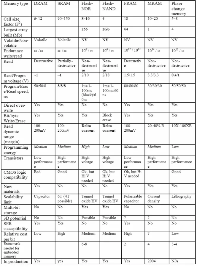
Table 1.1 Performance comparison between volatile memory (DRAM & SRAM) and nonvolatile memory (Flash, FRAM, and PCM) devices. Flash memory exhibits the best performance except the disadvantages of high programming voltage and slow program/erase speed.
Chapter 2
Table 2.1 Suggested bias conditions for the 2 bits/cell memory operation of the PrO2
nanocrystal memory condition.
Chapter 3
Table 3.1 Suggested bias conditions for the 2 bits/cell memory operation of the LaAlO3
FIGURE CAPTIONS
Figure Captions
Chapter 1
Fig. 1.1 MOS memory tree.
Fig. 1.2 The structure of the conventional floating gate nonvolatile memory device. Continuous poly-Si floating gate is used as the charge storage element.
Fig. 1.3 Comparison between the poly-silicon floating gate memory and SONOS memory. (a) Energy band diagram during retention in the poly-Si FG memory device. φ0 =
3.15 eV. (b) Energy band diagram during retention in the nitride trap-based memory. A typical Et value is between 0.8 to 1.1 eV below Ec . φ0 = 3.15 eV.
Chapter 2
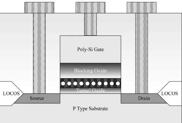
Fig. 2.1 Schematic cross section of the PrO2 nanocrystal memory device.
Fig. 2.2 Ids-Vds curves of the PrO2 memory. A memory window of larger than 2V can be
achieved with Vg=Vd=7V programming operation.
Fig. 2.3 (a) Program characteristics with different programming conductions. The program time can be short as 1ms and a memory window of about 3V can be achieved for Vg=Vd=9V. (b) Erase characteristics for different erase conductions.
Fig. 2.4 Retention characteristics of the PrO2 nanocrystal memory devices at T=25℃、85℃
and 125℃.
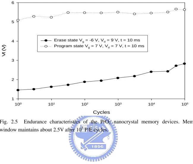
Fig. 2.5 Endurance characteristics of the PrO2 nanocrystal memory devices. Memory
window maintains about 2.5V after 105 P/E cycles.
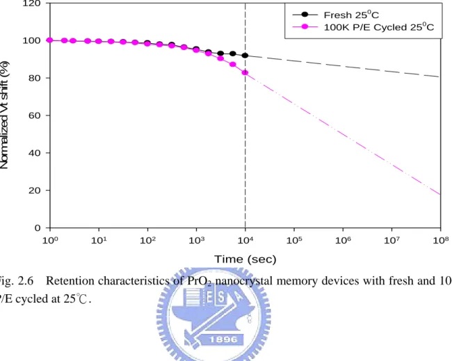
Fig. 2.6 Retention characteristics of PrO2 nanocrystal memory devices with fresh and 100K
P/E cycled at 25℃.
Fig. 2.7 Ids-Vgs curves of the PrO2 nanocrystal memory devices in 2-bit per cell operation,
forward read and reverse read for programmed bit 1 and programmed bit 2.
Fig. 2.8 Retention characteristics of the PrO2 nanocrystal memory devices for Programmed
bit-1 and erased bit-2 at room temperature.
Fig. 2.9 Drain disturbance characteristics of the PrO2 nanocrystal memory devices. After
1000s stress at 25℃, only less than 1V drain disturbance be observed for Vd=9V
condition.
Fig. 2.10 Gate disturbance characteristics of the PrO2 nanocrystal memory devices. After
1000s stress at 25℃, only less than 0.5V gate disturbance be observed for Vg=9V
FIGURE CAPTIONS
Fig. 2.11 Read disturbance characteristics of the PrO2 nanocrystal memory devices. After
1000s stress at 25℃, only less than 0.4V read disturbance be observed for Vg=4V, Vd=4V condition.
Chapter 3
Fig. 3.1 Schematic cross section of the LaAlO3 nanocrystal memory device.
Fig. 3.2 Ids-Vds curves of the LaAlO3 memory. A memory window of larger than 4V can be
achieved with Vg=Vd=7V programming operation.
Fig. 3.3 (a) Program characteristics with different programming conductions. The program time can be short as 0.1ms and a memory window of about 3V can be achieved for Vg=Vd=9V. (b) Erase characteristics for different erase conductions.
Fig. 3.4 Retention characteristics of the LaAlO3 nanocrystal memory devices at T=25℃、
85℃ and 125℃.
Fig. 3.5 Endurance characteristics of the LaAlO3 nanocrystal memory devices. Memory
window maintains about 2.5V after 104 P/E cycles.
Fig. 3.6 Retention characteristics of LaAlO3 nanocrystal memory devices with fresh and
10K P/E cycled at 25℃ and 85℃, respectively.
Fig. 3.7 Ids-Vgs curves of the LaAlO3 nanocrystal memory devices in 2-bit per cell
operation, forward read and reverse read for programmed bit 1 and programmed bit 2.
Fig. 3.8 Retention characteristics of the LaAlO3 nanocrystal memory devices for
Programmed bit-1 and erased bit-2 at room temperature.
Fig. 3.9 Drain disturbance characteristics of the LaAlO3 nanocrystal memory devices. After
1000s stress at 25℃, the drain disturb voltage of about 1V be observed for Vd=9V
condition.
Fig. 3.10 Gate disturbance characteristics of the LaAlO3 nanocrystal memory devices. After
1000s stress at 25℃, only less than 1V gate disturbance be observed for Vg=9V
condition.
Fig. 3.11 Read disturbance characteristics of the LaAlO3 nanocrystal memory devices. After
1000s stress at 25℃, only less than 1V read disturbance be observed for Vg=3.5V,
CHAPTER 1
Introduction
1.1 General Background
The semiconductor market has been continuously increasing for a long term, and this
growing trend is expected to continue in the coming years. About 20 % of this market is given
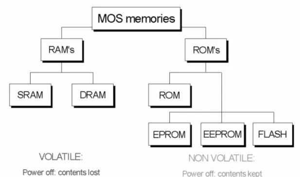
by the semiconductor memory, which can be divided into two main categories: random access
memories (RAM’s) and read-only memories (ROM’s). Both are based on the complementary
metal-oxide-semiconductor (CMOS) technology. For RAM’s, like SRAM and DRAM, that
although very fast in writing and reading for SRAM or very dense for DRAM, which are
nonvolatile, i.e., they lose stored information once the power supply is switched off. For
ROM’s, like EPROM, EEPROM, or Flash, are able to balance the less-aggressive
programming and reading performances with nonvolatile character, i.e., with the capability to
keep stored information even without power supply (Fig. 1.1).
In recent years, portable electronic products have widely applied, such as digital camera,
mobile PC, cellular phone, mp3 audio player, intelligent IC card, USB Flash personal disc,
and so on. These products are all based on nonvolatile memory. Moreover, in the coming
years, portable systems will demand even more nonvolatile memories, the density and
operation speed and reliability become the most important research theme. Today, Flash sales
represent a considerable amount of the overall semiconductor market. There are two major
applications for Flash memories that should be pointed out. One application is the possibility
of nonvolatile memory integration in logic system-mainly, but not only, microprocessors-
to allow software updates, store identification codes, reconfigure the system on the field, or
boards or solid-state hard disks, made by Flash memory arrays which are configured to create
large-size memories to compete with miniaturized hard disks. Solid-state disks are very useful
for portable applications, since they have small dimensions, low power consumption, and no
mobile parts, therefore being more robust. Flash combine the capability of nonvolatile storage
with an access time comparable to DRAM’s, which allows direct execution of microcodes. If
this is going happen, Flash memory will compete for the same market share with DRAM.
Moreover, Flash memories can find interesting applications in personal computer program
management: many programs can be stored in Flash chips, without being continuously loaded
and unloaded from hard disk partitions, and directly executed.
In 1960’s, due to high cost, large volume, and high power consumption of the
magnetic-core memory, the electronic industries urgently needed a new kind of memory
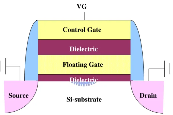
device to replace the magnetic-core memory. In 1967, D. Kahng and S. M. Sze invented the
floating-gate (FG) nonvolatile semiconductor memory at Bell Labs [1]. A Flash memory cell
is basically a floating-gate MOS transistor (Fig. 1.2), i.e., a transistor with a gate completely
surrounded by dielectrics, the floating gate, and electrically governed by a capacitively
coupled control gate (CG). Figure 1.2 shows the cross-section of an industry-standard Flash
cell. This cell structure was presented for the first time by Intel in 1988 and named ETOX
(EPROM Tunnel Oxide). The operation principal is using the polycrystalline silicon as FG to
be the charge stored units for the cell device. After electrons which injected from channel, the
threshold voltage of devices will be shifted. The logical “0” and “1” definition of nonvolatile
memory devices are used for the difference between threshold voltages.
The invention of FG nonvolatile memory creates a huge industry of portable electronic
systems, and is widely used in both standalone and embedded memories up to today. Flash
memory is presently the most suitable choice for nonvolatile applications for following
consists of only one transistor [2]. A FeRAM1 memory cell generally consists of one transistor
and one capacitor [3], while a MRAM cell needs a transistor and a magnetic tunnel junction
[4]. Phase change memory (PCM) was expected to be a promising nonvolatile memory [5];
however, its memory cell consists of one resistor and a bipolar junction transistor. Until now,
only a 4 MB PCM chip has been demonstrated. It will take more effort to demonstrate
whether PCM is really a promising technology. Second, Flash memory fabrication process is
compatible with the current CMOS process and is a suitable solution for embedded memory
applications. A Flash memory cell is simply a MOSFET cell, except that a poly-silicon
floating gate is sandwiched between a tunnel oxide and an inter-poly oxide to form a charge
storage layer [6]. All other nonvolatile memories require integration of new materials that are
not as compatible with a convention CMOS process. It is easier and more reliable to integrate
flash memory than other nonvolatile memories with logic and analog devices in order to
achieve better chip performance for wireless communication and wireless computation.
Although conventional FG memories have many advantages over other kinds of
nonvolatile memories, it still comes to be in face of their limitations form scaling issues for
the coming generations. Table 1.1 shows performance comparison between volatile memory
and nonvolatile memory. For conventional floating-gate memories, which offer longer than
ten years of retention time, have the drawbacks of high operation voltage and slow
program/erase because of their relatively thick tunnel oxide. Although poly-silicon used as the
charge storage layer in Flash memories is a very reliable material and is fully compatible with
the current CMOS process flow. However, poly-silicon shows some intrinsic disadvantages
and thus may not be the ultimate charge storage material for scaled Flash memory technology.
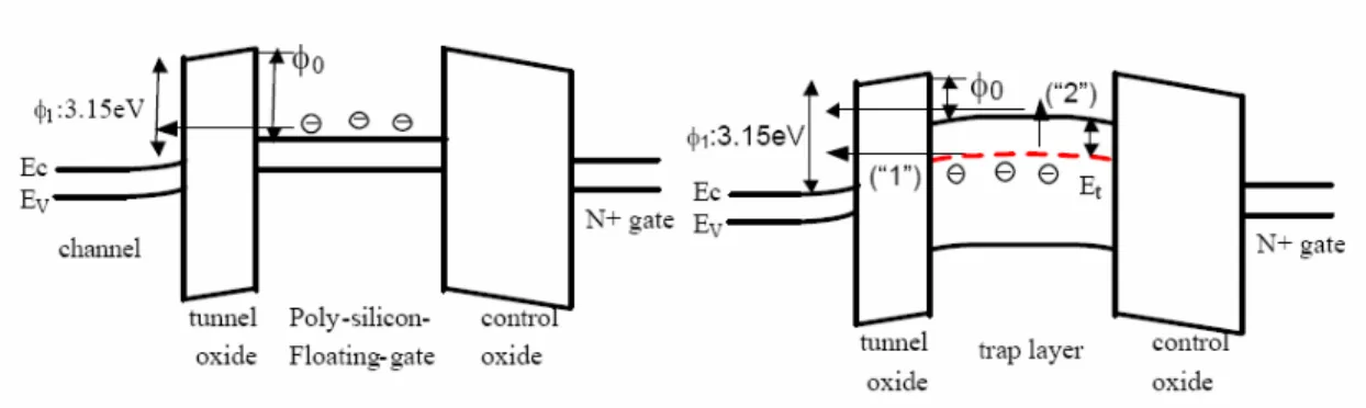
Figure 1.3(a) shows the energy band diagram of a FG Flash memory device during retention,
electrons are stored in the conduction band of the poly-silicon FG. There are two main
1
FeRAM is not a perfect nonvolatile memory since its reading mode is destructive. A programming verification is required to restore the data after reading.
disadvantages for using poly-silicon as the charge storage layer. First, electrons impinge to the
tunnel oxide/floating gate interface very frequently, thereby having a large tendency to leak
back to the channel, this is known as the escape frequency. Second, since poly-silicon is a
conducting material, electrons can move freely in the conduction band. If there is a defect
chain within the tunnel oxide, all of trapped electrons in the floating gate can easily leak to the
channel or source/drain thought it. This is why a very thick tunnel oxide (>7 nm) is required
to reduce leakage probability. Unfortunately, a thick tunnel oxide requires a high operation
voltage for program/erase, the power consumption must become high, the speed of the
operation will be slower, and there is a difficulty in scaling down. But when the thinner tunnel
oxide is be considered, the retention characteristics will be degraded. There is a tradeoff
between speed and reliability.
To overcome the scaling limits of the conventional FG structure, other kinds of
nonvolatile memories such as SONOS [7]-[9] and nanocrystal memories [10]-[12] which
stored electrons in discrete traps are mostly mentioned. The basic idea of the “discrete-trap”
mechanism is to replace the floating gate of nonvolatile memories by many discrete trapping
centers, which can be made by natural traps in an appropriate insulator (a nitride layer in
SONOS memories) or by semiconductor (usually silicon) nanocrystals. Charges trapped in
discrete trap centers are more immune to the leakage caused by localized oxide defects, thus
allowing more aggressive scaling of the tunnel oxide and exhibit superior characteristics
compared to conventional FG memories in terms of operation voltage, write/erase speed, and
endurance [13], [14]. The energy band diagram of a nitride trap-based memory (SONOS
memory) is shown in Figure 1.3(b). In SONOS memory, electrons are stored in the physically
discrete traps (labeled with the trap energy level of Et) below the nitride conduction band [15],
[16]. In this device, electrons can not move freely between discrete trap locations, hence
endurance than the FG memory. In retention mode, electrons can leak to the channel through
the direct tunneling process shown as path (1) in Fig. 1.3(b). However, in this device the
escape frequency is very small. Alternatively, electrons can be thermally de-trapped into the
nitride conduction band and then tunnel back to the channel, shown as path (2) in the figure.
This thermal de-trapping rate is exponentially reduced with a deep trap energy level. For these
reasons, SONOS memory has much better retention time than FG memory. A tunnel oxide of
3 nm is thick enough to achieve 10 years retention time in SONOS memory and lower the
power consumption. Moreover, the discreteness of the charge traps enables multibit-per-cell
storage [17], [18] without going through the multilevel approach, which poses stringent
requirement on the control of threshold spread [19]. Besides mentioned above, there are
several major potential advantages of discrete-trap memories as follow:
1) Suppression of cells with abnormally short retention time, it is known as “erratic
bits”.
2) Suppression of the drain-turn phenomenon, being one of the major limiting factors of
NOR device scaling, due to the absence of drain-to-floating-gate coupling, allowing
for higher drain voltages during read-out, shorter channel length and, consequently,
smaller cell area.
3) Decreased capacitance coupling ratios, eliminating the main problem of floating-gate
interference in ultradense NAND devices.
4) Simple, low-cost device fabrication because no dual-poly complex process is needed.
1.2
Motivation
Aggressive scaling of the semiconductor memory cells and the dramatic increase in the
structure. However, conventional FG structure with thick tunnel oxide is much slower to
program and has poor endurance. In order to improve the write/erase speed of memory, the
thickness of the tunnel oxide must be reduced. The tunnel oxide must be less than 25 Å to
achieve 100 ns write/erase time for a reasonable programming voltage (<10 V) [20].
Unfortunately, the retention time will be too short then. Stress induced leakage current (SILC)
will further degrade the retention time.
To alleviate the tunnel oxide design tradeoff for FG memory devices, the charge storage
property of semiconductor nanocrystals embedded in a silicon oxide matrix is currently under
intense investigation due to its potential application in future nonvolatile memories.
Nanocrystal charge storage offers several potential advantages over conventional stacked-gate
nonvolatile memory. First, the use of isolated nanocyrstals for charge storage improved
retention resulting from Coulomb blockade [21] and quantum confinement effects (bandgap
widening, energy quantization) that enable the use of thinner tunnel oxides and reduce the
programming and erasing voltages [11], [22]. Second, the charges loss through lateral paths in
nanocrystal type memories can be suppressed by the oxide isolation between nanocrystals,
thus exhibited superior charge storage characteristics compared with conventional FG
memory, and can provide opportunities for 2bits/cell operation. Third, due to the area savings
from memory module peripheral voltage scaling and the reduction in mask count over
conventional FG technology, nanocrystal nonvolatile memory technology can substantially
reduce the cost of embedded Flash at the 90 nm technology node and beyond. Fourth, reduced
punch-through achieved by eliminating drain-to-floating-gate coupling, allowing higher drain
voltages during readout, shorter channel lengths, and smaller cell area. Fifth, nanocrystal
memories show excellent immunity to SILC and defects within the FG or insulating layers
due to the distributed nature of the charge storage in the discontinuous nanocrystal layer.
employed LPCVD to fabricate Si nanocrystals with 4.5 nm average size and area density 5 ×
1011 cm-2 [23]. King et al. fabricated Ge nanocrystals by oxidation of a Si1-xGex layer formed
by ion implantation, and demonstrated quasi-nonvolatile memory operation with a 0.4 V
threshold voltage shift [24]. Kanjilal et al. demonstrated a sheet of spherical, well-separated,
crystalline Ge nano-dots embedded in SiO2 on top of p-(001) Si wafer, fabricated by
molecular beam epitaxy (MBE) combined with rapid thermal processing and characterized
structurally and electrically [25]. The potential for improved device performance and
reliability strongly depends upon the ability to control particle core size, particle size
distribution, crystallinity, areal particle density, oxide-passivation quality, and
crystal-to-crystal insulation that prevents lateral charge conduction in the nanocrystal layer.
From mentioned above, we attempt to fabricate nanocrystal memories using high-k
dielectric materials such as LaAlO3 and PrO2. These materials provide high trapping state
densities and deep trapping levels, thus they can enhance the characteristic of retention, the
operation voltage can be reduced and large operation window can be achieved simultaneously.
1.3
Organization of the Thesis
There are four chapters in this thesis. In chapter 1, we describe the background of Flash
memory, its applications and development, advantages and disadvantages, challenges and
motivation for semiconductor nanorcryatal nonvolatile memories.
In chapter 2, we use Dual E-Gun Evaporation System to deposit thin PrO2 layer, the wafer
was subjected to RTA treatment to form nanocrystal, subsequently. The electrical
characteristics of nanocrystal memory devices by using PrO2 as nanocrystal material are
investigated.
wafer was subjected to RTA treatment to form nanocrystal, subsequently. The electrical
characteristics of nanocrystal memory devices by using Lanthanum aluminate (LaAlO3) as
nanocrystal material are investigated.
Finally, in chapter 4, the conclusions are made and the recommendation describes the
Table 1.1 Performance comparison between volatile memory (DRAM &
SRAM) and nonvolatile memory (Flash, FRAM, and PCM) devices. Flash
memory exhibits the best performance except the disadvantages of high
programming voltage and slow program/erase speed.
VG
Si-substrate
Source
Drain
Dielectric
Floating Gate
Control Gate
Dielectric
Fig. 1.2 The structure of the conventional floating gate nonvolatile memory
device. Continuous poly-Si floating gate is used as the charge storage element.
Fig. 1.3 Comparison between the poly-silicon floating gate memory and SONOS memory. (a) Energy band diagram during retention in the poly-Si FG memory device. φ0 = 3.15 eV. (b)
Energy band diagram during retention in the nitride trap-based memory. A typical Et value is between 0.8 to 1.1 eV below Ec . φ0 = 3.15 eV.
CHAPTER 2
Characteristics of Nanocrystal Flash Memory
by Using PrO
2high-
κ
Material
2.1 Introduction
In this chapter, we try to fabricate nanocrystal nonvolatile memory by using a high-κ material which is praseodymium oxide (PrO2) as charge trapping centers. Now, PrO2 has
investigated as an alternative high-κ gate dielectric material for silicon integrated circuits, which has outstanding dielectric properties. Some excellent characteristics can be summarized as follows: First, an effective dielectric constant value of around 30, independent of the substrate doping type. Second, relative low leakage current density with respect to HfO2 or
ZrO2 film with the same effective oxide thickness (EOT), which can be explained by heavy
electron masses in the oxide due to localized electrons forming the lowest conduction bands. Third, PrO2 exhibits symmetrical band offsets larger 1 eV to Si. Fourth, praseodymium oxide
exhibits excellent reliability characteristics based on measurements of current density as a function of gate voltage and stress induced leakage current (SILC), even after stresss-induced electrical breakdown. Fifth, there is no serious degradation in structural and electrical properties after annealing in CMOS typical process. For these superior characteristics better than other high-κ materials, making praseodymium oxide an attractive candidate as gate dielectric for next generation.
In this work, we have successfully fabricated a nonvolatile memory embedded PrO2
nanocrystals for the first time. This material provides high trapping state density, therefore large operation window can be achieved. The use of high-k material as nanocrystals can
reduce tunneling oxide and blocking oxide thickness, thus the operation voltage can be decreased and maintains superior retention characteristic, and improves memory device scaling down. It has good characteristics in terms of considerably large memory window, high program/erase speed, good endurance, and good disturbance.
2.2 Experimental Details
Figure 2.1 schematically describes the process flow of the PrO2 nanocrystal nonvolatile
memory. The fabrication process of this memory device was started with LOCOS isolation process on a p-type, 5-10 Ω‧cm, (100) 150 nm silicon substrate. For the first step, a 2-nm-thick tunnel oxide was thermally grown at 925℃ in furnace system. A praseodymium oxide layer was subsequently deposited on the oxide by Dual E-gun Evaporation System with Praseodymium oxide targets. The deposition of praseodymium layer is a critical process to decide the size of the nanocrystal. E-gun deposition rate is relied on adjustment of the current magnitude by a remote control. After that, the wafer was subjected to RTA treatment in O2
ambient at 900℃ for 1 minute. When the film is RTA treated to provide enough energy and surface mobility, the thin Praseodymium oxide will self-assemble into a lower-total-enough state. An 15 nm blocking oxide was then deposited by Plasma Enhanced Chemical Vapor Deposition (PECVD) followed by a N2 densification process at 800℃ for 1 min. A
200-nm-thick poly-Si was deposited succeeding by LPCVD to serve as gate electrode. Subsequently, gate patterning, S/D implanting, and the remaining standard CMOS procedures were completed to fabricate the PrO2 nanocrystal nonvolatile memory devices.
2.3 Results and Discussions
In this thesis, all devices described had dimensions of L/W = 1/10 µm, and the threshold voltage is defined when the Ids current reach 10-7 A in Ids-Vds curves.
2.3.1 Characteristics of Flash Devices
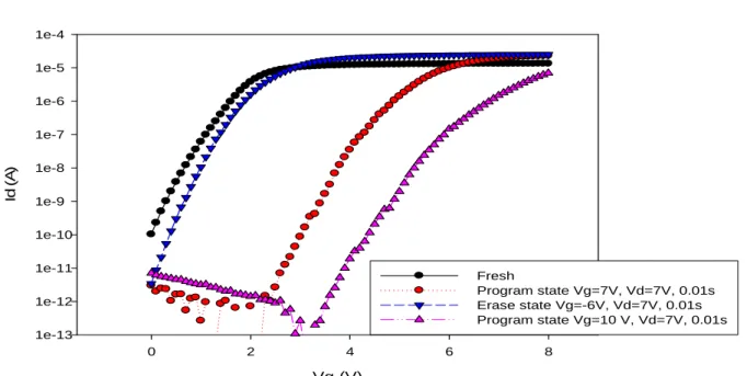
Figure 2.2 shows the Ids-Vds curve of the PrO2 nanocrystal nonvolatile memory device
under fresh, programmed and erased states. Channel hot-electron injection and band-to-band hot-hole injection were employed for programming and erasing, respectively. The programming and erase time are both 10 ms, and a memory window of about 2V can be clearly observed. For Vg=Vd=10V, program time is also 10 ms, a memory window larger than
4V can be easily achieved. During programming, a small fraction of electrons in the substrate obtain enough energy from applied voltage Vd to surmount the barrier between oxide and
silicon conduction band edges. These electrons can be trapped in PrO2 nanocrystals and the
threshold voltage shift to right. When erasing, we applied a positive drain voltage Vd to
generate hot hole in the subject and a large enough negative gate voltage to across the energy barrier. It reduces the threshold voltage and causes the Ids-Vds curve shift to left. We use this
mechanism of adjust threshold voltage by different applied voltages to obtain memory characteristics.
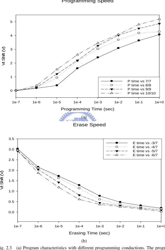
The program and erase speed is shown in Fig. 2.3. The “Vt Shift” is defined as threshold
voltage difference between the program state and erase state. Gate and drain terminals were biased equally from 7 to 10V. Both source and substrate terminals were biased at 0V. As shown in Fig. 2.3(a), program characteristics as a function of pulse width. With Vg and Vd
increasing, the Vth shift increases and the program speed becomes faster. The program time
can be short as 1ms and a memory window of about 3V can be achieved for Vg=Vd=9V. Fig.
2.3(b) shows the erase characteristics of the PrO2 nanocrystal nonvolatile memory for
different conditions: Vg=-3, -4, -5, -6V with the same Vd=7V. We can easily find similar
phenomenon like programming, the Vth decrease faster as the applied gate voltage be more
negative biased. Excellent erase speed of around 1ms can be obtain for Vg=-6V, Vd=7V. A
This is owing to the fact that the vertical electric field decreases with decreasing amount of trapped electrons in the trapping layer during erasing and the hole injection into the trapping layer will reduce significantly [26].
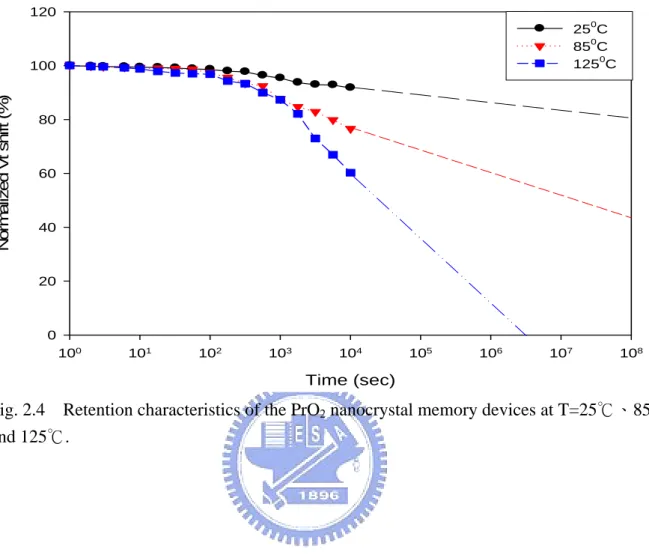
Fig. 2.4 illustrates the retention characteristics of PrO2 nanocrystal memory devices for
comparing different temperature (T=25℃、85℃ and 125℃). The retention time can be up to 108 seconds for 20% charge loss at room temperature, which is belived to be related to the deep trap energy level in the high-k nanocrystal [27]. Furthermore, the quality of the tunneling oxide plays a significant role in charge retention. It’s a pity that the retention go worst as the temperature increased [28]-[32].
The endurance characteristics after 105 P/E cycles of the PrO2 nanocrystal memory
devices are shown in Fig. 2.5. The programming and erasing conduction are Vg=Vd=7V for
10ms, Vg=-6, Vd=9V for 10ms, respectively. Small amount increase of the threshold voltages
in programmed and erased state can be observed. This is due to the mismatch between the localized spatial distributions for injected electron and holes by using channel hot-electron programming and band-to-band hot-hole erasing. The uncompensated electrons cause to increase the threshold voltage in erase state over P/E cycling [33]. For another reason, This may be the stress-induced electron traps generated in the tunneling oxide during cycling [34].
The cycling retention is also an important issue for memory. Fig. 2.6 shows the retention characteristics compare with fresh and 100K P/E cycled at 25℃. We can find that the charge loss behavior of the devices with 100K cycling is more serious than the other. This means the tunneling oxide damaged after 100K P/E cycling, thus stress-induced electron trapping in the tunneling oxide increases and the charge storage capability decreases, the retention characteristics go worst.
2.3.2 Characteristics of 2-bit Operation
Fig. 2.7 demonstrates the feasibility of 2-bit operation for the PrO2 nanocrystal memory
devices. From the Ids-Vgs curves, we can employ forward and reverse reads for detecting the
information stored in programmed bit1 and bit2, respectively. Table 3.1 summarizes suggested bias conditions for the 2 bits per cell operation. The retention characteristics for 2-bit operation is shown in Fig. 2.8. A memory window larger than 1.5 V until 108 seconds can be observed. Furthermore, we discovered that charge loss occurred both for programmed bit-1 and erased bit-2, it was represented that there is a vertical migration of the trapped electron [35].
2.3.3 Disturbance Measurement
Fig. 2.9 shows the programming drain disturb characteristics of the PrO2 memory. Drain
disturbance may influence programmed memory to reduce the threshold voltage during programming. In our measurement, three different drain voltages (Vd=5, 7 and 9V) and
Vg=Vs=Vb=0V were applied in the programming drain disturbance measurement at room
temperature (T=25℃). We found that even after stressed at Vd=9V for 1000s, the program
drain disturbance is not obvious (△Vt < 1V).
Fig. 2.10 shows the gate disturb characteristics in the erasing state. While a cell is being programmed, gate disturbance may occur for the cells sharing a common word line. The applied gate voltage attracts electrons in the substrate to tunnel to the PrO2 nanocrystal, thus
induce the threshold voltage to shift rightward. In this experiment, three different gate voltages (Vg=7, 8 and 9V) were applied to simulate the program situation which the cell
unselected. A threshold voltage shift of only 0.3V at Vg=9V for 1000s was observed, it means
that gate disturbance almost can be negligible.
the applied bit line voltage in reverse read must be sufficiently large (> 2V in our samples) to be able to “read through” the trapped charge in the neighbor bit. The voltage during read operation could cause unwanted electron injection, called “soft-programming” [36], induces erase state threshold voltage to convert into program state of the neighbor bit by the cumulative low level injections. There are two major factors causing the threshold voltage instability: the voltages of the word line and the bit line. The word line voltage during reading may enhance room temperature drift in the neighbor bit, and the bit line voltage during reading may cause unwanted channel hot electron injection and result in the threshold voltage shift subsequently. In our measurements, the gate voltage was applied at 4V, the drain voltages were applied at 2, 3 and 4V, respectively, both the source and the substrate were grounded. No apparent read disturbance is observed (△Vt < 0.4V) for samples after
stressing 1000s at 25℃.
2.4 Summary
In this chapter, we have investigated the memory effects and performance of the PrO2
nanocrystal memory devices. From our discussion, the memory has good characteristics in terms of large memory windows, low applied voltages, high program/erase speed, good retention at room temperature, excellent endurance, 2-bit operation and fine disturbances. Consequently, PrO2 is a potential candidate for nanocrystal material in nanocrystal memory
Ids-Vgs Curves Vg (V) 0 2 4 6 8 Id (A ) 1e-13 1e-12 1e-11 1e-10 1e-9 1e-8 1e-7 1e-6 1e-5 1e-4 Fresh Program state Vg=7V, Vd=7V, 0.01s Erase state Vg=-6V, Vd=7V, 0.01s Program state Vg=10 V, Vd=7V, 0.01s
Fig. 2.2 Ids-Vds curves of the PrO2 memory. A memory window of larger than 2V can be
Programming Speed
Programming Time (sec)
1e-7 1e-6 1e-5 1e-4 1e-3 1e-2 1e-1 1e+0
Vt Sh if t ( V ) 0 1 2 3 4 5 P time vs 7/7 P time vs 8/8 P time vs 9/9 P time vs 10/10 (a) Erase Speed
Erasing Time (sec)
1e-7 1e-6 1e-5 1e-4 1e-3 1e-2 1e-1 1e+0
Vt Sh if t ( V ) 0.0 0.5 1.0 1.5 2.0 2.5 3.0 3.5 E time vs -3/7 E time vs -4/7 E time vs -5/7 E time vs -6/7 (b)
Fig. 2.3 (a) Program characteristics with different programming conductions. The program time can be short as 1ms and a memory window of about 3V can be achieved for Vg=Vd=9V.
Retention Characteristics Time (sec) 100 101 102 103 104 105 106 107 108 N o rm a liz e d V t s h ift ( % ) 0 20 40 60 80 100 120 250C 850C 1250C
Fig. 2.4 Retention characteristics of the PrO2 nanocrystal memory devices at T=25℃、85℃
Endurance Characteristics Cycles 100 101 102 103 104 105 Vt ( V ) 1 2 3 4 5 6 Erase state Vg = -6 V, Vd = 9 V, t = 10 ms Program state Vg = 7 V, Vd = 7 V, t = 10 ms
Fig. 2.5 Endurance characteristics of the PrO2 nanocrystal memory devices. Memory
Retention Characteristics Time (sec) 100 101 102 103 104 105 106 107 108 N o rm a liz e d V t s h ift ( % ) 0 20 40 60 80 100 120 Fresh 250C 100K P/E Cycled 250C
Fig. 2.6 Retention characteristics of PrO2 nanocrystal memory devices with fresh and 100K
Ids-Vgs Curves Vg (V) 0 1 2 3 4 5 6 7 8 Id ( A ) 10-10 10-9 10-8 10-7 10-6 10-5 10-4 (Bit 1, Bit 2)=(1,1), Vd=0.1 V, Vs=0 V
(Bit 1, Bit 2)=(0,1), forward read for Bit 1, Vd=0.1 V, Vs=0 V (Bit 1, Bit 2)=(0,1), reverse read for Bit 1, Vd=2 V, Vs=0 V (Bit 1, Bit 2)=(1,0), forward read for Bit 2, Vd=0 V, Vs=0.1 V (Bit 1, Bit 2)=(1,0), reverse read for Bit 2, Vd=0 V, Vs=2 V
Fig. 2.7 Ids-Vgs curves of the PrO2 nanocrystal memory devices in 2-bit per cell operation,
forward read and reverse read for programmed bit 1 and programmed bit 2.
Program Erase Read
Vg 7 V -6 V 4 V Vd 7 V 8 V 0 V Bit 1 Vs 0 V 0 V >2 V Vg 7 V -6 V 4 V Vd 0 V 0 V >2 V Bit 2 Vs 7 V 8 V 0 V
Table. 2.1 Suggested bias conditions for the 2 bits/cell memory operation of the PrO2
Retention Characteristics for 2-bit operation Time (sec) 100 101 102 103 104 105 106 107 108 Vt ( V ) 2 3 4 5 Programmed bit-1 Erased bit-2 T = 25 0C
Fig. 2.8 Retention characteristics of the PrO2 nanocrystal memory devices for Programmed
Drain Disturbance Characteristics Time (sec) 1 10 100 1000 P rogr a m s tat e V t-s hi ft ( V ) -2 -1 0 1 2 Vd=5 Vd=7 Vd=9
Fig. 2.9 Drain disturbance characteristics of the PrO2 nanocrystal memory devices. After
1000s stress at 25℃, only less than 1V drain disturbance be observed for Vd=9V condition. Gate Disturbance Characteristics
Time (sec) 1 10 100 1000 E ras e s tat e V t-s hi ft ( V ) -1.0 -0.5 0.0 0.5 1.0 Vg=7 Vg=8 Vg=9
Fig. 2.10 Gate disturbance characteristics of the PrO2 nanocrystal memory devices. After
Read Disturbance Characteristics Time (sec) 1 10 100 1000 E ras e s tat e V t-s hi ft ( V ) -2 -1 0 1 2 Vg=4 Vd=2 Vg=4 Vd=3 Vg=4 Vd=4
Fig. 2.11 Read disturbance characteristics of the PrO2 nanocrystal memory devices. After
1000s stress at 25℃, only less than 0.4V read disturbance be observed for Vg=4V, Vd=4V
CHAPTER 3
Characteristics of Nanocrystal Flash Memory
by Using LaAlO
3high-
κ
Material
3.1 Introduction
The scaling down of silicon integrated circuits has pushed conventional SiO2 gate
dielectric films close to its physical limit. When the SiO2 physical thickness becomes thinner
than about 3 nm, direct tunneling through the dielectric barrier dominates the leakage current. Substitution of silicon dioxide with high dielectric constant thin films as the gate dielectrics for sub-100 nm CMOS devices has received increasing attention [37]. Numerous materials are being considered as replacements for SiO2 as the gate dielectric in future MOSFETs. The
materials most commonly proposed to replace SiO2 are metal oxides such as Ta2O5 [38], ZrO2
[39], HfO2 [40], TiO2 [41], etc. Unfortunately, until to now, none of the materials can meet all
the requirements of alternative gate dielectric [37].
Lanthanum aluminate (LaAlO3) has been extensively used as the substrate and buffer
layer for high-temperature superconductors [38]. It is well known that La2O3 has a
high-dielectric constant and Al2O3 has a good thermal stability. LaAlO3, as a compound of
La2O3 and Al2O3, may combine their desirable chemical and electrical properties while
eliminating the deficiencies of each material. It seems that LaAlO3 may have a great potential
as an alternative gate dielectric material to replace SiO2 in next-generation MOSFET
application.
In this work, we have successfully fabricated a nonvolatile memory embedded LaAlO3
nanocrystals for the first time. This material provides high trapping state density, therefore large operation window can be achieved. The use of high-κ material as nanocrystals can
reduce tunneling oxide and blocking oxide thickness, thus the operation voltage can be decreased and maintains superior retention characteristic, and improves memory device scaling down. It has good characteristics in terms of considerably large memory window, high program/erase speed, good endurance, and good disturbance.
3.2 Experimental Details
Figure 3.1 schematically describes the process flow of the LaAlO3 nanocrystal
nonvolatile memory. The fabrication process of this memory device was started with LOCOS isolation process on a p-type, 5-10 Ω‧cm, (100) 150 nm silicon substrate. For the first step, a 2-nm-thick tunnel oxide was thermally grown at 925℃ in furnace system. A lanthanum aluminate (LaAlO3) film was subsequently deposited on the oxide by Dual E-gun Evaporation
System with lanthanum aluminate targets. The deposition of lanthanum aluminate is a critical process to decide the size of the nanocrystal. The deposition rate of Dual E-gun Evaporation System is relied on adjustment of the current magnitude by a remote control. After that, the wafer was subjected to RTA treatment in O2 ambient at 900℃ for 1 minute. When the film is
RTA treated to provide enough energy and surface mobility, the thin lanthanum aluminate film will self-assemble into a lower-total-enough state. An 15 nm blocking oxide was then deposited by Plasma Enhanced Chemical Vapor Deposition (PECVD) followed by a O2
densification process at 800℃ for 1 min. A 200-nm-thick poly-Si was deposited succeeding by LPCVD to serve as gate electrode. Subsequently, gate patterning, S/D implanting, and the remaining standard CMOS procedures were completed to fabricate the LaAlO3 nanocrystal
nonvolatile memory devices.
3.3 Results and Discussion
voltage is defined when the Ids current reach 10-7 A in Ids-Vds curves.
3.3.1 Characteristics of Flash Devices
Figure 3.2 shows the Ids-Vds curve of the LaAlO3 nanocrystal nonvolatile memory device
under fresh, programmed and erased states. Channel hot-electron injection and band-to-band hot-hole injection were employed for programming and erasing, respectively. The programming and erase time are both 1 ms, and a memory window of about 4V can be clearly observed. For Vg=Vd=10V, program time is also 1 ms, a memory window larger than 5.5V
can be easily achieved. During programming, a small fraction of electrons in the substrate obtain enough energy from applied voltage Vd to surmount the barrier between oxide and
silicon conduction band edges. These electrons can be trapped in LaAlO3 nanocrystals and the
threshold voltage shift to right. When erasing, we applied a positive drain voltage Vd to
generate hot hole in the subject and a large enough negative gate voltage to across the energy barrier. It reduces the threshold voltage and causes the Ids-Vds curve shift to left. We use this
mechanism of adjust threshold voltage by different applied voltages to obtain memory characteristics.
The program and erase speed is shown in Fig. 3.3. Gate and drain terminals were biased equally from 7 to 10V. Both source and substrate terminals were biased at 0V. As shown in Fig. 3.3(a), program characteristics as a function of pulse width. With Vg and Vd increasing,
the Vth shift increases and the program speed becomes faster. The program time can be short
as 0.1ms and a memory window of about 3V can be achieved for Vg=Vd=9V. Fig. 3.3(b)
shows the erase characteristics of the LaAlO3 nanocrystal nonvolatile memory for different
conditions: Vd=6, 7 ,8V with the same Vg=-3V. We can easily find similar phenomenon like
programming, the Vth decrease faster as the applied drain voltage be more positive biased.
Excellent erase speed of around 0.1ms can be obtain for Vg=-3V, Vd=8V. The same
don’t take place. The smaller voltage be applied at the gate terminal of the LaAlO3
nanocrystal memory devices, the vertical electric field decreases with decreasing amount of trapped electrons in the trapping layer during erasing and the hole injection into the trapping layer will reduce significantly.
Fig. 3.4 illustrates the retention characteristics of LaAlO3 nanocrystal memory devices for
comparing different temperature (T=25℃、85℃ and 125℃). The retention time can be up to 108 seconds for 20% charge loss at room temperature, which is belived to be related to the deep trap energy level in the high-k nanocrystal [27]. Furthermore, the quality of the tunneling oxide plays a significant role in charge retention.
The endurance characteristics after 104 P/E cycles of the LaAlO3 nanocrystal memory
devices are shown in Fig. 3.5. The programming and erasing conduction are Vg=Vd=7V for
0.1ms, Vg=-7, Vd=8V for 1ms, respectively. Small amount increase of the threshold voltages
in programmed and decrease of those in erased state can be observed. This is due to the mismatch between the localized spatial distributions for injected electron and holes by using channel hot-electron programming and band-to-band hot-hole erasing. The uncompensated electrons cause to increase the threshold voltage in erase state over P/E cycling [33]. For another reason, This may be the stress-induced electron traps generated in the tunneling oxide during cycling [34].
The cycling retention is also an important issue for memory. Fig. 3.6 shows the retention characteristics compare with fresh and 10K P/E cycled at 25℃ and 85℃, respectively. We can find that the charge loss behavior of the devices with 10K cycling, but not obvious. This is because decrease of the program and erase time. The tunneling oxide damaged after 10K P/E cycling is not serious, stress-induced electron trapping in the tunneling oxide increases and the charge storage capability decreases, the retention characteristics go worst a little bit.
3.3.2 Characteristics of 2-bit Operation
Fig. 3.7 demonstrates the feasibility of 2-bit operation for the LaAlO3 nanocrystal memory
devices. From the Ids-Vgs curves, we can employ forward and reverse reads for detecting the
information stored in programmed bit1 and bit2, respectively. Table 3.1 summarizes suggested bias conditions for the 2 bits per cell operation. The retention characteristics for 2-bit operation is shown in Fig. 3.8. A memory window larger than 1 V until 108 seconds can be observed. Furthermore, we discovered that charge loss occurred both for programmed bit-1 and erased bit-2, it was represented that there is a vertical migration of the trapped electron [35].
3.3.3 Disturbance Measurement
Fig. 3.9 shows the programming drain disturb characteristics of the LaAlO3 memory.
Drain disturbance may influence programmed memory to reduce the threshold voltage during programming. In our measurement, three different drain voltages (Vd=5, 7 and 9V) and
Vg=Vs=Vb=0V were applied in the programming drain disturbance measurement at room
temperature (T=25℃). We found that even after stressed at Vd=9V for 1000s, the program
drain disturbance is not obvious (△Vt < 1V).
Fig. 3.10 shows the gate disturb characteristics in the erasing state. While a cell is being programmed, gate disturbance may occur for the cells sharing a common word line. The applied gate voltage attracts electrons in the substrate to tunnel to the LaAlO3 nanocrystal,
thus induces the threshold voltage to shift rightward. In this experiment, three different gate voltages (Vg=7, 8 and 9V) were applied to simulate the program situation which the cell
unselected. A threshold voltage shift of only 0.3V at Vg=9V for 1000s was observed, it means
that gate disturbance almost can be negligible.
the applied bit line voltage in reverse read must be sufficiently large (> 2V in our samples) to be able to “read through” the trapped charge in the neighbor bit. The voltage during read operation could cause unwanted electron injection, called “soft-programming” [36], induces erase state threshold voltage to convert into program state of the neighbor bit by the cumulative low level injections. There are two major factors causing the threshold voltage instability: the voltages of the word line and the bit line. The word line voltage during reading may enhance room temperature drift in the neighbor bit, and the bit line voltage during reading may cause unwanted channel hot electron injection and result in the threshold voltage shift subsequently. In our measurements, the gate voltage was applied at 3.5V, the drain voltages were applied at 2, 3 and 4V, respectively, both the source and the substrate were grounded. No apparent read disturbance is observed (△Vt < 1V) for samples after stressing
1000s at 25℃.
3.4 Summary
In this chapter, we have investigated the memory effects and performance of the LaAlO3
nanocrystal memory devices. From our discussion, the memory has good characteristics in terms of large memory windows, low applied voltages, high program/erase speed, good retention at room temperature, excellent retention, 2-bit operation and fine disturbances. Consequently, LaAlO3 is a potential candidate for nanocrystal material in fabricating
Ids-Vgs Curves Vg (V) 0 2 4 6 8 Id ( A ) 1e-13 1e-12 1e-11 1e-10 1e-9 1e-8 1e-7 1e-6 1e-5 1e-4 1e-3 Fresh Program state Vg=7V, Vd=7V, 0.001s Erase state Vg=-6V, Vd=8V, 0.001s Program state Vg=10 V, Vd=10V, 0.001s
Fig. 3.2 Ids-Vds curves of the LaAlO3 memory. A memory window of larger than 4V can be
Programming Speed
Programming Time (sec)
1e-7 1e-6 1e-5 1e-4 1e-3 1e-2 1e-1 1e+0
Vt Sh if t ( V ) 0 1 2 3 4 5 P time vs 7/7 P time vs 8/8 P time vs 9/9 P time vs 10/10 (a) Erase Speed
Erasing Time (sec)
1e-7 1e-6 1e-5 1e-4 1e-3 1e-2 1e-1 1e+0
Vt Sh if t ( V ) 0 1 2 3 4 E time vs -3/6 E time vs -3/7 E time vs -3/8 (b)
Fig. 3.3 (a) Program characteristics with different programming conductions. The program time can be short as 0.1ms and a memory window of about 3V can be achieved for Vg=Vd=9V.
Retention Characteristics Time (sec) 100 101 102 103 104 105 106 107 108 N o rm a liz e d V t s h ift ( % ) 0 20 40 60 80 100 120 time vs 25C time vs 85C time vs 125C
Fig. 3.4 Retention characteristics of the LaAlO3 nanocrystal memory devices at T=25℃、
Endurance Characteristics Cycles 100 101 102 103 104 Vt ( V ) 1 2 3 4 5 6 Erase state Vg = -7 V, Vd = 8 V, t = 10 ms Program state Vg = 7 V, Vd = 7 V, t = 10 ms
Fig. 3.5 Endurance characteristics of the LaAlO3 nanocrystal memory devices. Memory
Retention Characteristics Time (sec) 100 101 102 103 104 105 106 107 108 N o rm a liz e d V t s h ift ( % ) 0 20 40 60 80 100 120 time vs 25C time vs 85C time vs 25C, 10k time vs 85C, 10k
Fig. 3.6 Retention characteristics of LaAlO3 nanocrystal memory devices with fresh and
Ids-Vgs Curves Vg (V) 0 1 2 3 4 5 6 7 8 Id ( A ) 10-12 10-11 10-10 10-9 10-8 10-7 10-6 10-5 10-4 (Bit 1, Bit 2)=(1,1), Vd=0.1 V, Vs=0 V
(Bit 1, Bit 2)=(0,1), forward read for Bit 1, Vd=0.1 V, Vs=0 V (Bit 1, Bit 2)=(0,1), reverse read for Bit 1, Vd=2 V, Vs=0 V (Bit 1, Bit 2)=(1,0), forward read for Bit 2, Vd=0 V, Vs=0.1 V (Bit 1, Bit 2)=(1,0), reverse read for Bit 2, Vd=0 V, Vs=2 V
Fig. 3.7 Ids-Vgs curves of the LaAlO3 nanocrystal memory devices in 2-bit per cell operation,
forward read and reverse read for programmed bit 1 and programmed bit 2.
Program Erase Read
Vg 7 V -6 V 3.5 V Vd 7 V 8 V 0 V Bit 1 Vs 0 V 0 V >2 V Vg 7 V -6 V 3.5 V Vd 0 V 0 V >2 V Bit 2 Vs 7 V 8 V 0 V
Table. 3.1 Suggested bias conditions for the 2 bits/cell memory operation of the LaAlO3
Retention Characteristics of 2-bit operation Time (sec) 100 101 102 103 104 105 106 107 108 Vt ( V ) 2 3 4 5 Programmed bit-1 Erased bit-2 T = 25 0C
Fig. 3.8 Retention characteristics of the LaAlO3 nanocrystal memory devices for
Drain Disturbance Characteristics Time (sec) 1 10 100 1000 P rogr a m s tat e V t-s hi ft ( V ) -2 -1 0 1 2 Vd=5 Vd=7 Vd=9
Fig. 3.9 Drain disturbance characteristics of the LaAlO3 nanocrystal memory devices. After
1000s stress at 25℃, the drain disturb voltage of about 1V be observed for Vd=9V condition. Gate Disturbance Characteristics
Time (sec) 1 10 100 1000 E ras e s tat e V t-s hi ft ( V ) -2 -1 0 1 2 Vg=9 Vg=8 Vg=7
Fig. 3.10 Gate disturbance characteristics of the LaAlO3 nanocrystal memory devices. After
Read Disturbance Characteristics Time (sec) 1 10 100 1000 E ras e s tat e V t-s hi ft ( V ) -2 -1 0 1 2 Vg=3.5 Vd=2 Vg=3.5 Vd=3 Vg=3.5 Vd=4
Fig. 3.11 Read disturbance characteristics of the LaAlO3 nanocrystal memory devices. After
1000s stress at 25℃, only less than 1V read disturbance be observed for Vg=3.5V, Vd=4V
CHAPTER 4
Conclusion and Recommendations for Future Works
4.1 Conclusions
The thesis of “Characteristics and Investigation of Next Generation Low Power Flash
Memory Devices” was proposed. In this thesis, we have investigated a novel, simple,
reproducible, reliable technique for preparation of high density PrO2 and LaAlO3 nanocrystal
memory devices, and it is compatible to conventional CMOS process. The results of each
chapter are summarized as below:
In chapter 2, we have successfully fabricated a nonvolatile memory embedded PrO2
nanocrystals. This material provides high trapping state density, therefore large operation
window can be achieved. The samples of PrO2 nanocrystal memory devices have several
good electrical performance such as: low applied voltages, large memory window, high
program/erase speed, good retention characteristic, excellent endurance, 2-bit operation and
fine disturb characteristics. Consequently, PrO2 is a potential candidate for nanocrystal
material in nanocrystal memory devices.
In chapter 3, we have investigated a nonvolatile memory embedded LaAlO3 nanocrystals.
Originally, LaAlO3 has been extensively used as the substrate and buffer layer for
high-temperature superconductors. In recent years, LaAlO3 be considered as an alternative
gate dielectric material combining advantages of La2O3 and Al2O3 to replace SiO2 for the next
generation. We first fabricated the nanocrystal memory devices by using LaAlO3 materials,
which have good characteristics in terms of low applied voltages, large memory window, high
up to 10K P/E cycles, 2-bit operation and fine disturb characteristics.
4.2 Recommendations for Future Works
1) More HRTEM images to evidence nanocrystal formation and thickness variation of
tunneling oxide and blocking oxide.
2) More physical analyses to quantitatively understand nanocrystal composition and
interaction.
3) Advanced analyze methods can be measurement, such like charge pumping
characteristics, migration of storage charges (vertical and lateral migration),
activation energy.
4) Other oxides of Lanthanide series and high-κ materials can be try to form nanocrystals due to self-assemble characteristic.
5) Other manufacturing method can be try, such like deposition of high-κ material and SiO2 simutaneously.
References
[1] D. Kahan and S. M. Sze, “A floating gate and its application to memory devices”, Bell
Syst. Tech, J., 46, 1288, 1967.
[2] Seiichi Aritome, “Advanced Flash memory technology and trends for files storage
Application”, IEDM 2000, pp. 763-766.
[3] D. J. Jung, B, G, Jeon, and H. H. Kim, “Highly manufacturable 1T1C 4Mb FRAM with
novel sensing scheme” IEDM 2000, pp. 279-282.
[4] “Advanced memory technology and architecture” short course, IEDM 2001.
[5] S. Lai and T. Lowrey, “OUM - A 180 nm nonvolatile memory cell element technology
for stand alone and embedded applications”, IEDM 2000, pp. 36.5.1-36.5.4.
[6] Takuya Kitamura et al, “A low voltage operating Flash memory cell with high coupling
ratio using horned floating gate with fine HSG”, pp. 104-105, 1998 Symposium on VLSI
Technology.
[7] M. H. White, D. A. Adams, and J. Bu, “On the go with SONOS”, IEEE circuits &
devices, vol. 16, issue 4, pp. 22-31, July 2000.
[8] M. H. White, Y. Yang, A. Purwar, and M. L. French, “A low voltage SONOS nonvolatile
semiconductor memory technology”, IEEE Components, Packaging, and Manufacturing
Technology, Part A, vol. 20, issue 2, pp. 190-195, June 1997.
[9] J. K. Bu, M. H. White, “Design considerations in scaled SONOS nonvolatile memory
devices”, Solid State Electronics, vol.45, pp. 113-120, Jan. 2001.
[10] S. Tiwari, F. Rana, K. Chan, H. Hanafi, C. Wei, and D. Buchanan, “Volatile and
non-volatile memories in silicon with nano-crystal storage”, IEEE Int. Electron Devices
[11] J. J. Welser, S. Tiwari, S. Rishton, K. Y. Lee, and Y. Lee, “Room temperature operation
of a quantum-dot flash memory”, IEEE Electron Device Lett., 18, 278, 1997.
[12] Y. C. King, T. J. King, and C. Hu, “MOS memory using germanium nanocrystals formed
by thermal oxidation of Si1-xGex”, IEEE Int. Electron Devices Meeting Tech. Dig., 115,
1998.
[13] H. I. Hanafi, S. Tiwari, and I. Khan, “Fast and long retention-time nanocrystal memory,”
IEEE Trans. Electron Devices, vol. 43, pp. 1553-1558, Sept. 1996.
[14] Y.-C. King, T.-J. King, and C. Hu, “Charge-trap memory device fabricated by oxidation
of Si1-xGex,” IEEE Trans. Electron Devices, vol. 48, pp. 696-700, Apr. 2001.
[15] H. Aozasa, I. Fujiwara, A. Nakamura and Y. Komatsu, “Analysis of Carrier Traps in
Si3N4 in Oxide/Nitride/Oxide for Metal/Oxide/Nitride/Oxide Silicon Nonvolatile
Memory”, Japanese Journal of Applied Physics, vol.38, part 1, no.3A, pp. 1441-1447,
1999.
[16] Y. Yang and M. H. White, “Charge retention of scaled SONOS nonvolatile memory
devices at elevated temperatures”, Solid State Electronics, vol.44, pp. 949-958, 2000.
[17] B. Eitan, P. Pavan, I. Bloom, E, Aloni, A. Fromer, and D. Finzi, “NROM: A novel
localized trapping, 2-bit nonvolatile memory cell,” IEEE Electron Device Lett., vol. 21,
pp. 543-545, Nov. 2000.
[18] Z. Liu, C. Lee, V. Narayanan, G. Pei, and E. C. Kan, “Nanocrystal memories with
multibit-per-cell storage,” J. Solid-State Circuits, to be published.
[19] B. Eitan, R. Kazerounian, A. Roy, G. Crisenza, P. Cappelletti, and A. Modelli,
“Multilevel flash cells and their trade-offs,” in IEDM Tech. Dig., 1996, pp. 169-172.
[21] H. Grabert and M. H. Devoret, Single Charge Tunneling: Coulomb Blockade Phenomena
in Nanostructures. New York: Plenum, 1992.
[22] S. Tiwari, F. Rana, K. Chan, L. Shi, and H. Hanafi, “Single charge and confinement
effects in nanocrystal memories,” Appl. Phys. Lett. Vol.69, pp. 1232-1234.
[23] I. Kim, S. Han, J. Lee, and H. Shin, “Room temperature single electron effects n a Si
nano-crystal memory,” IEEE Electron Device Lett.
[24] Y. King, T. J. King, and C. Hu, “MOS memory using Germanium nanocrystals formed
by therman oxidation of Si1-xGex,” in IEDM Tech. Dig., 1998, p. 115.
[25] R. Phba, N. Sugiyama, K. Uchida, J. Koga, and A. Toriumi, “Nonvolatile Si quantum
memory with self-aligned doubly-stacked dots,” IEEE Trans. Electron Devices, vol.49,
pp. 1392, 2002.
[26] Susanne Stemmer, Zhiqiang Chen, Carlos G. Levi, Patrick S. Lysaght, Brendan Foran,
John A. Gisby, and Jeff R. Taylor, “Application of metastable phase diagrams to silicate
thin films for alternative gate dielectircs,” Jpn. J. Appl. Phys., vol.42, pp. 3593-3597,
2003.
[27] M. L. Ostraat, J. W. De Blauwe, M. L. Green, L. D. Bell, M. L. Brongersma, J.
Casperson, R. C. Flagan, and H. A. Atwater, “Synthesis and characterization of aerosol
silicon nanocrystal nonvolatile floating-gate memory devices,” Appl. Phys. Lett., vol. 79,
pp. 433-435, 2001.
[28] T. S. Chen, K. H. Wu, H. Chung, and C. H. Kao, “Performance improvement of SONOS
memory by bandgap engineer of charge-trapping layer,” IEEE Electron Device Lett., vol.
25, no. 4, pp. 205-207, Apr. 2002.
[29] “Test and test equipment” in The International Technology Roadmap for Semiconductors
[30] T. Sugizaki, M. Kobayashi, H. Minakata, M. Yamaguchi, Y. Tamura, Y. Sugiyama, H.
Tanaka, T. Nakaanishi, and Y. Nara, “New 2-bit/Tr MONOS type flash memory using
Al2O3 as charge trapping layer,” in Proc. IEEE Non-Volatile Semiconductor Memory
Workshop, Feb. 2003, pp. 60-61.
[31] Y. N. Tan, W. K. Chim, W. K. Choi, M. S. Joo, T. H. Ng, and B. J. Cho, “High-k HfAlO
charge trapping layer in SONOS-type nonvolatile memory device for high speed
operation,” in IEDM Tech. Dig., 2004, pp. 889-892.
[32] Barbara De Salvo, Gerard Ghibaudo, Georges Pananakakis, Gills Reimbold, Francois
Mondond, Bernard Guillaumot,and Philippe Candelier, “Experimental and theoretical
investigation of nonvolatile memory data-retention,” IEEE Trans. Electron Devices, vol.
46, no. 7, pp. 1518-1524, Jul., 1999.
[33] Yu-Hsien Lin, Chao-Hsin Chien, Ching-Tzung Lin, Ching-Wei Chen, Chun-Yen Chang,
and Tan-Fu Lei, “High Performance Multi-bit Nonvolatile HfO2 Nanocrystal Memory
Using Spinodal Phase Separation of Hafnium Silicate,” IEDM Technical Digest, pp.
1080-1082, Dec. 2004.
[34] Y. H. Lin, C. H. Chien, C. T. Lin, C. Y. Chang, and T. F. Lei, “High Performance
Nonvolatile HfO2 Nanocrystal Memory,” IEEE Electron Device Lett., vol. 26, no. 3, pp.
154-156, Mar. 2005.
[35] T. Sugizaki, M. Kobayashi, M. Ishidao, H. Minakata, M. Yamaguchi, Y. Tamura, Y.
Sugiyama, T. Nakanishi, H. Tanaka, “Novel multi-bit SONOS type flash memory using a
high-k charge trapping layer,” VLSI Technology, 2003. Digest of Technical Papers. 2003
Symposium, pp.27-28, June 2003.
[36] Van Houdt J. F., Wellekens D., Groeseneken G. and Maes H. E., “Investigation of the
Device Lett., vol. 16, p. 181, 1995.
[37] G. D. Wilk, R. M. Wallace and J. M. Anthony, J. Appl. Phys. Vol. 89, p. 5243, 2001.
[38] P. K. Roy and I. C. Kizilyalli, Appl. Phys. Lett., vol. 72, p. 2835, 1998.
[39] M. Copel, M. A. Gribelyuk and E. Gusev, Appl. Phys. Lett., vol. 76, pp. 436, 2000.
[40] B. H. Lee, L. Kang, R. Nieh, W. J. Qi and J. C. Lee, Appl. Phys. Lett., vol. 76, pp. 1926,
2000.
[41] R. B. van Dover, Appl. Phys. Lett., vol. 74, pp. 3041, 1999.
[42] A. E. Lee, C. E. Platt, J. F. Burch, R. W. Simon, J. P. Goral and M. M. Al-Jassim, Appl.