Mechanism for Cu void defect on various electroplated film conditions
H.P. Feng
a, M.Y. Cheng
b, Y.L. Wang
c,*, S.C. Chang
c, Y.Y. Wang
a, C.C. Wan
a aDepartment of Chemical Engineering, National Tsing Hua University, Hsinchu, Taiwan
b
Department of Materials Science and Engineering, National Chiao Tung University, Hsinchu, Taiwan
c
College of Science and Engineering, National University of Tainan, Taiwan Available online 24 August 2005
Abstract
This study observes that copper (Cu) films deposited by high current densities or in an aged electrolyte easily generate void defects after chemical mechanical polishing (CMP). The (111)/(200) ratio and the impurity amount of an electroplated Cu film are found to have strong correlation with the formation of void defects. Furthermore, pulse-reverse waveform plating following direct current plating is used for the deposition of partial Cu films that will be exposed after Cu CMP. This new scheme produces a void-less Cu surface after CMP.
D 2005 Elsevier B.V. All rights reserved.
Keywords: Copper plating; Copper void; Direct current plating; Electromigration resistance
1. Introduction
In most semiconductor processes nowadays, electro-plating has been adopted by industry as the primary deposition method for copper (Cu) metallization. Grain size, impurity and texture of polycrystalline Cu films are known to be critical factors in determining interconnect qualities such as film resistivity and electromigration resistance. The grain structure and impurity content of deposited films strongly relate to electroplating conditions and sequential annealing procedures. Hara et al.[1]reported that the resistivity of Cu layers was determined mainly by the grain size and stress. Rapid variation of the grain growth rate was based on stress development. The defect (dis-location/vacancy) density within the film decreased through grain growth [2,3]. Typically, face-centered-cubic (fcc) Cu films have a preferred (111) crystallographic orientation that is through to be desirable for improving the reliability of metal interconnections [4,5]. For fcc metal films, the orientation with the lowest surface energy is (111) while that with the lowest elastic strain energy is (100)[6,7]. The
texture of Cu films can transform to high (100)/(111) ratio during grain growth (grain growth induced stress), or through thermal annealing (thermally induced stress) [8,9]. Recently, Haper et al. suggested that impurities that were incorporated into the film, such as carbon and sulfur of the plating bath, were initially pinning the grain boundaries
[10]. These impurities were coalesced, thus enabling some of grain boundaries to move.
Recent researches have shown that void defects of Cu thin films mainly yield killers and seriously degrade interconnect reliability. It is believed that good Cu film quality indeed improves void defects. This paper inves-tigates the roles of grain textures and film impurities on the formation of Cu voids after chemical mechanical polishing (CMP).
2. Experimental details
Blanket wafers used in this study were 8-in. Si (100) wafers with 100-nm thermal oxide/30-nm TaN/150-nm Cu seed layers, where TaN and Cu seed layers were deposited by physical vapor deposition (PVD) at room temperature without vacuum breaking. Patterned wafers with different line widths were generated by optical lithography and 0040-6090/$ - see front matterD 2005 Elsevier B.V. All rights reserved.
doi:10.1016/j.tsf.2005.07.062
* Corresponding author. Tel.: +886 6 5098069; fax: +886 6 5052081. E-mail address: ylwang@tsmc.com (Y.L. Wang).
Thin Solid Films 498 (2006) 56 – 59
anisotropic etch processes. Electroplating is carried out in a commercial plating system with small amounts of propri-etary organic additives from Shipley. Two series of Cu films were plated: (1) 1-um-thick films plated with direct current (DC) at 10, 30 and 80 mA/cm2, (2) 1-um-thick films plated with pulse-reverse (PR) current (the waveform is 10 s normal current and 1 s reverse current by five times of normal value) 10, 30 and 80 mA/cm2. The variation of plating current distribution across wafer is controlled below 3%. The post-electroplating annealing was performed at 220 -C with 60 s.
The grain sizes of Cu films were determined by focus ion beam (FIB) electron microscopy. The textures of Cu films were examined by X-ray diffraction (XRD). The impurities in Cu films including carbon, oxide, sulfur and chloride atoms were detected by secondary ion mass spectrometer (SIMS) analysis. Optical scan method (KLA)
was used to detect Cu film defects after CMP. Varying defect types are determined by scanning electron micro-scopy (SEM) reviewing.
3. Results and discussion
Fig. 1shows that a Cu film deposited by high current
density has more void defects after CMP as compared with that by low current density. These defects are easily formed at grain boundaries of Cu films, as shown in Fig. 2. Based on material sciences, grain boundaries are weaker points for chemical attacking during the CMP process. However, it is interesting to find that the amount of grain boundaries is not the key factor for the formation of void defects because identical Cu grain size is found after thermal annealing for various plating current
Fig. 2. FIB image of void defects on an electroplated Cu film in DC plating current 80 mA/cm2. 1 10 100 1000 0 204 06 08 0 100 120
Void Defect versus Film Texture
Void Defect Count (ea)
(111)/(200) Texture (b) (a) 120 100 100 80 80 60 60 40 40 20 20 0 0 (111)/(200) Ratio
Plating current density (mA/cm2)
DC PR
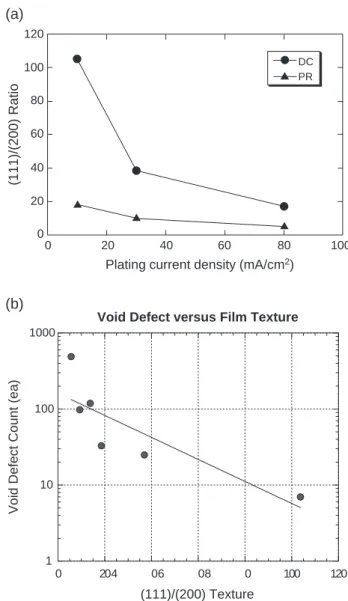
Fig. 3. (a) Value of (111)/(200) ratio versus plating current densities for DC and PR plating, (b) amount of void defects versus (111)/(200) ratios. 0 100 200 300 400 500 600 0 20 40 60 80 100
Void Defect Number (ea)
Current Density (mA/cm2) PR plating waveform DC plating waveform
Fig. 1. Void defect counts versus plating current densities.
densities. There may be other causes to dominate the defect results.
Fig. 3(a) reveals that an increase in the plating current densities decreases the (111)/(200) ratio of Cu films no matter using DC or PR. Moreover, the PR plating generates higher (111)/(200) ratio than the DC plating. In this case, all Cu films are thermal annealed at 220-C with 60 s after electroplating. It is also found that the amount of void defects decreases as the (111)/(200) ratio increases, as shown in Fig. 3(b). For fcc thin films, the (111) texture is favored by the surface and interfacial energy minimization, whereas the (200) texture is favored by the strain energy minimization. After thermal annealing, the observed textures may result from a competition between these mechanisms as mentioned. It is suggested that the (111) texture has higher chemical resistance than other planes of the fcc structure because (111) is the closed packed plane in the fcc structure.
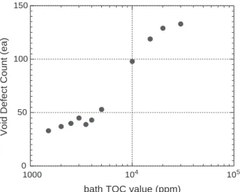
Besides film textures, the impurities from a plating bath may influence the chemical resistance of deposited Cu films. As the bath ages, certain byproducts are formed from additive decomposition during plating process [11]. The amount of total organic concentration (TOC) implies the accumulation of organic byproducts in a plating bath
[12]. The more bath byproducts induced, the more impurities incorporated into the deposited films. Fig. 4
shows that the count of void defects is proportional to the bath TOC value. On the other hand, the higher plating current density generates higher impurity level (carbon) in deposited Cu films, as shown the SIMS results of Fig. 5(a) and (b). Notably, there are compatible impurity levels in the Cu films deposited by DC 80 mA/cm2 and PR 80 mA/cm2. But PR 80 mA/cm2generates fewer void defects than DC 80 mA/cm2 implying that the film texture has higher correlation than the impurity level with the formation of Cu void defects.
On the other hand, using PR current waveform or lower DC current density can reduce void defects after CMP. Due to the throughput concern for production, the combination of PR waveforms, low plating current and high plating current is used in this study to reduce the void defects while maintaining a complete filling. Fig. 6(a) displays the schematic diagram of Cu electroplating, which part A is deposited by the high current density for throughput concern and is a sacrifice layer for CMP, while part C is deposited by the low current density for gap-filling concern and is responsible to electronic trans-ferring. The high current film in the interface of trench structure induces void defects possibly due to its weaker chemical resistance. Fig. 6(b) shows a novel scheme of Cu
108 107 106 105 104 103 102 101 100 108 107 106 105 104 103 102 101 100 [c/s] [c/s] 100 100 300 300 500 500 700 700 Sput. Time : [s] Sput. Time : [s] 12C 12C 12C 12C 12C 12C C-Pulse-80mA C-Pulse-10mA C-Pulse-30mA C-DC-80mA C-DC-30mA C-DC-10mA
Fig. 5. SIMS measurements of (a) carbon in the Cu film deposited by DC plating waveform, (b) carbon in the Cu film deposited by PR plating waveform. 0 50 100 150 1000 104 105
Void Defect Count (ea)
bath TOC value (ppm)
Fig. 4. Void defect count versus bath TOC (ppm) in DC plating current 10 mA/cm2.
H.P. Feng et al. / Thin Solid Films 498 (2006) 56 – 59 58
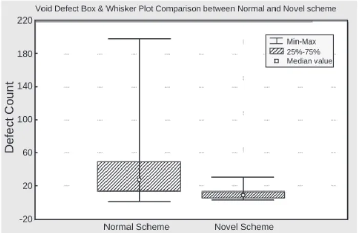
electroplating, which part B is deposited by PR plating and used to be the interface between part A and part C. Part B will be exposed after Cu CMP and reduces void defects. Finally, defect reliability test can be performed to reveal the effect of current density that using 30 wafers both in novel scheme and normal scheme for KLA-optical defect scan after CMP. Fig. 7 is the box plot to show that the novel method apparently reduces the 80% void defect after Cu CMP as compared with the normal scheme.
4. Conclusions
An increase in plating current densities easily generates void defects on Cu surfaces after CMP. The amount of grain boundaries is not the key factor whereas the film texture is found to be the dominant element for the formation of void defects. The (111)/(200) ratio increases with decreasing the plating current densities. An increase in the (111)/(200) ratio also benefits the reduction of void defects after Cu CMP. The result is suggested that the (111) texture has higher chemical resistance during Cu CMP. In addition, an increase in film impurities resulted from an aging bath or higher plating current densities lead to more void defects possibly due to a decrease in chemical resistance of Cu films by impurity incorporation. Furthermore, the PR waveform is used in this study to
improve the defect performance while maintaining the gap-filling capability and throughput.
Acknowledgments
The authors would like to thank the National Science Council of the Republic of China, Taiwan, for partially supporting this research under Contract no. NSC93-2216-E009-015. Technical supports from Taiwan Semiconductor Manufacturing Company are also appreciated.
References
[1] T. Hara, H. Toida, Y. Shimura, J. Electrochem. Soc. 6 (2003) G98. [2] H.L. Wei, R.K. Zheng, G.H. Wen, X.X. Zhang, Appl. Phys. Lett. 80
(2002) 2290.
[3] H. Lee, S.S. Wong, S.D. Loptain, J. Appl. Phys. 93 (2003) 3796. [4] Q.T. Jiang, M.E. Thomas, J. Vac. Sci. Technol., B 19 (2001) 762. [5] S.M. Rossnagel, T.S. Kuan, J. Vac. Sci. Technol., A 20 (2002) 1911. [6] C. Detavernier, D. Deduytsche, R.L. Van Meirhaeghe, J. De
Baerdemaeker, C. Dauwe, Appl. Phys. Lett. 82 (2003) 1863. [7] E.M. Zielinski, R.P. Vinci, J.C. Bravman, J. Appl. Phys. 76 (1994)
4515.
[8] J.A. Thornton, J. Vac. Sci. Technol. 12 (1975) 830. [9] K.R. Hebert, J. Electrochem. Soc. 148 (2001) C726.
[10] S. Nakayama, A. Kimura, M. Shibata, S. Kuwabata, T. Oskai, J. Electrochem. Soc. 148 (2001) B467.
[11] L. Vanasupa, Y.C. Joo, P.R. Besser, J. Appl. Phys. 85 (1999) 2583. [12] M.W. Lane, C.E. Murray, F.R. McFeely, P.M. Vereecken, R.
Rosenberg, Appl. Phys. Lett. 83 (2003) 2330.
220 180 140 100 60 20 -20 Normal Scheme Defect Count
Void Defect Box & Whisker Plot Comparison between Normal and Novel scheme
Novel Scheme
Min-Max 25%-75% Median value
Fig. 7. Box and Whisker Plot comparison between conventional and novel schemes for the formation of void defects.
High current density film Low current density film
High current density film Low current density film PR current density film
Part A Part C (a) Part A Part C Part B (b)
Fig. 6. (a) Conventional plating scheme and (b) novel plating scheme for damascene gap-filling.