IEEE ELECTRON DEVICE LETTERS, VOL. 28, NO. 9, SEPTEMBER 2007 809
A Novel Nanowire Channel Poly-Si TFT Functioning
as Transistor and Nonvolatile SONOS Memory
Shih-Ching Chen, Ting-Chang Chang, Po-Tsun Liu, Yung-Chun Wu, Po-Shun Lin, Bae-Heng Tseng,
Jang-Hung Shy, S. M. Sze, Chun-Yen Chang, and Chen-Hsin Lien
Abstract—In this letter, a polycrystalline silicon thin–film tran-sistor consisting of silicon–oxide–nitride–oxide–silicon (SONOS) stack gate dielectric and nanowire (NW) channels was investi-gated for the applications of transistor and nonvolatile mem-ory. The proposed device, which is named as NW SONOS-TFT, has superior electrical characteristics of transistor, including a higher drain current, a smaller threshold voltage (Vth), and a
steeper subthreshold slope. Moreover, the NW SONOS-TFT also can exhibit high program/erase efficiency under adequate bias operation. The duality of both transistor and memory device for the NW SONOS-TFT can be attributed to the trigate structure and channel corner effect.
Index Terms—Nanowire (NW), nonvolatile memory, polysilicon (poly-Si), silicon–oxide–nitride–oxide–silicon (SONOS), thin-film transistor (TFT).
I. INTRODUCTION
P
OLYSILICON thin-film transistors (poly-Si TFTs) have attracted much attention for use in active-matrix liquid-crystal-displays since they can be integrated with peripheral driving circuits because of their high field effect mobility and driving current [1]. Systems-on-panels (SOP), which are integrated with such functional devices on an LCD panel as a controller [2] and memory [3], have been proposed in the development of display technology development to make dis-plays more compact and reliable and to reduce their cost. Since SOP technology is primarily used for portable electronics, low-power consumption is basically required to ensure long batteryManuscript received May 31, 2007; revised June 27, 2007. This work was supported in part by the National Science Council of China under Contracts NSC-95-2120-M-110-003 and NSC 95-2221-E-009-0254-MY2, and in part by MOEA Technology Development for Academia Project 95-EC-17-A-07-S1-046 and MOE ATU Program 95W803. The review of this letter was arranged by Editor J. Sin.
S.-C. Chen and C.-H. Lien are with the Institute of Electronics Engineering, National Tsing Hua University, Hsinchu 300, Taiwan, R.O.C.
T.-C. Chang is with the Department of Physics and Institute of Electro-Optical Engineering, and Center for Nanoscience and Nanotechnology, National Sun Yat-Sen University, Kaohsiung 804, Taiwan, R.O.C. (e-mail: [email protected]).
P.-T. Liu is with the Department of Photonics and Display Institute, National Chiao Tung University, Hsinchu 300, Taiwan, R.O.C.
Y.-C. Wu is with the Department of Engineering and System Science, National Tsing-Hua University, Hsinchu 300, Taiwan, R.O.C.
P.-S. Lin is with the Institute of Electro-Optical Engineering, National Sun Yat-Sen University, Kaohsiung 804, Taiwan, R.O.C.
B.-H. Tseng and J.-H. Shy are with the Institute of Materials Science and Engineering, National Sun Yat-Sen University, Kaohsiung 804, Taiwan, R.O.C. S. M. Sze and C.-Y. Chang are with the Institute of Electronics, National Chiao Tung University, Taiwan, Hsinchu 300, Taiwan, R.O.C.
Digital Object Identifier 10.1109/LED.2007.903885
life. It is well known that the nonvolatile memory is widely utilized for data storage in portable electronics systems due to its properties of low-power consumption and nonvolatil-ity. Unlike the conventional nonvolatile floating gate memory, silicon–oxide–nitride–oxide–silicon (SONOS)-type memory has become a promising candidate for SOP application because it is fully compatible with poly-Si TFTs process. However, SONOS-type nonvolatile memory still raises several issues concerning performance and reliability, such as insufficient programming/erasing (P/E) efficiency, poor endurance, and short retention time [4]. Recently, various approaches have been proposed for the improvement of the performance and reliability of SONOS using dielectric engineering [5], [6]. In addition, SONOS-type poly-Si TFT, which is fabricated by the sequential lateral solidified (SLS) method, has also been reported to improve the P/E efficiency by field-enhanced tun-neling in Si protrusion regions [7]. However, the uniformity of the Si protrusions recrystallized by SLS is still a problem.
Based on our previous study [8], the poly-Si TFT with nanowire (NW) channels can provide good gate control due to its trigate structure. Besides, the nonvolatile nanocrystal mem-ory with a narrow channel width structure has been demon-strated to improve the P/E efficiency [9]. Thus, in this letter, the poly-Si TFT combined with nonvolatile SONOS memory and NW channels, which is named as NW SONOS-TFT, is proposed to obtain superior electrical performance for transistor and higher P/E efficiency for memory device.
II. EXPERIMENT
In this letter, the SONOS-TFT with ten strips of 65-nm NW channel was proposed. The standard device with a single chan-nel structure with W = 1 µm (STD) was also fabricated for comparison. The detailed fabrication procedures are described as follows. At first, undoped amorphous silicon (a-Si) with thickness of 50 nm was deposited on oxidized silicon wafers by low-pressure chemical vapor deposition (LPCVD) at 550 ◦C. Then, the deposited a-Si layer was recrystallized by solid-phase crystallization at 600◦C for 24 h in a N2ambient. After the active region patterning by electron beam lithography, the 25-nm-thick ONO multilayer gate dielectric of the bottom oxide (5 nm) / silicon nitride (10 nm) / top oxide (10 nm) was deposited by LPCVD. Subsequently, a 150-nm-thick in situ n+ doped poly-Si layer was deposited and transferred to a gate electrode. After source/drain (S/D) formation by self-aligned phosphorous implantation, a 200-nm oxide passivation layer was deposited, and contact holes were patterned. Finally, Al
810 IEEE ELECTRON DEVICE LETTERS, VOL. 28, NO. 9, SEPTEMBER 2007
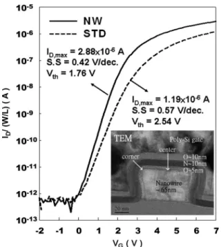
Fig. 1. Comparison of typical ID–VGcharacteristics of the standard and the
NW SONOS-TFTs. The inset exhibits the TEM of a single NW channel of NW SONOS-TFT.
metallization was performed, and the devices were sintered at 400◦C in nitrogen ambient for 30 min.
III. RESULTS ANDDISCUSSION
Fig. 1 presents the typical normalized ID–VGcurves of the
standard and the proposed NW SONOS-TFTs. The inset shows the transmission electron microscopy (TEM) photography of a single NW channel. It is clearly seen that the NW channel is surrounded by the control gate to form the trigate structure, and the physical channel width of NW SONOS-TFT is confirmed to be 65 nm. The threshold voltage in this letter is determined at
ID/(W/L) = 10 nA for VD= 0.1 V. The transfer
characteris-tic reveals that the NW device outperforms the standard device, with higher drain current, smaller threshold voltage (Vth), and steeper subthreshold swing. Since the effective channel width is increased, and the control of the channel region is enhanced by the trigate structure, the drain current and Vthcan be improved in NW SONOS-TFT. Furthermore, the current at the corner region turns on earlier than that at the surface of the channel because of the larger electrical field [10], and the additional corner current can increase the drain current as the number of corners increases. Hence, the enhancement in electrical performance of the NW SONOS-TFT can be attributed mainly to the good gate control by the trigate structure and the corner effect.
In addition, the SONOS-TFTs can also be used as nonvolatile memory devices at adequate gate voltage operation. However, the reset state Vth of memory differs from the Vth for the transistor due to gate injection into the ONO layer during an erasing operation. The reset state Vth is determined by the charge balance between the gate injection and the detrapping out of the ONO layer. Thus, the SONOS-TFT is not inter-changeable for the two modes at the same time. In this letter,
Fig. 2. Programming and erasing characteristics of memory devices for NW and standard structures.
Fig. 3. Simulation results of the electrical fields with a gate bias of 14 V for the standard device and NW device at center and corner regions.
due to the fact that tunneling current is mainly dominated by Fowler–Nordheim (FN) tunneling, as the thickness of tunnel-ing oxide is thicker than 5 nm [11], the SONOS-TFTs are programmed and erased by FN tunneling mechanism. Fig. 2 shows the programming and erasing characteristics of the NW and standard devices. Clearly, the memory device with multiple NW channels has greater P/E efficiency and memory window shift. For the standard device, the results also indicate that the memory windows are saturated as the programming time increases and the threshold voltage shift is very small even at a gate voltage of−14 V.
The distribution of an electrical field across the stacked gate dielectric was numerically simulated at a gate bias of 14 V using an ISE-TCAD simulator for the standard and NW devices to examine the improvement in the memory characteristics. As shown in Fig. 3, at the corners of the NW channel, the elec-trical field across the tunneling oxide is much larger than that across the blocking oxide. The P/E activity is thus facilitated between the tunneling oxide and channel rather than between the blocking oxide and the gate. Comparatively, electrical fields
CHEN et al.: NW CHANNEL POLY-Si TFT FUNCTIONING AS SONOS MEMORY 811
Fig. 4. (a) Endurance and (b) retention characteristic of the NW SONOS-TFT. Memory window remains 1.5 V after 104P/E cycles and 1 V after 106s
at 85◦C.
are uniformly across all oxide layers for the standard TFT device. This will lead the threshold voltage shift of the standard device to be easily saturated during the programming operation as soon as the equilibrium of electron flows is achieved through the paths from channel to the storage layer and from the storage layer to gate electrode. The injection of electrons from the gate to the storage layer during the erasing operation causes inefficient erasing and a lower threshold voltage shift in the standard device. Also, the inefficient erasing activity similarly appears at the center region of the NW channel. Therefore, the pronounced enhancement of P/E efficiency for the NW device is attributed to the large number of corners, where large electrical field is induced by the corner effect.
Fig. 4(a) shows the endurance characteristic of the NW device with a programming bias of 18 V for 1 ms and an erasing bias of −18 V for 1 s. Indeed, the memory window is degraded by interface-trap generation and tunneling oxide degradation as the number of P/E cycles increases. However, the NW device can still maintain a 1.5-V memory window after 106P/E cycles. The memory window is sufficiently large for the practical usability. Fig. 4(b) presents the retention characteristic of the NW device. The devices are programmed after 104P/E cycles and then measured at 85◦C. The result indicates that the memory window is still kept about 1 V after 106s at 85◦C.
IV. CONCLUSION
This letter demonstrates the feasibility of a novel poly-Si TFT that functions as both transistor and nonvolatile SONOS memory. The experimental results show that the NW SONOS-TFT has the better electrical characteristics because of its trigate structure and additional corner current that is induced by corner effect. In addition, the proposed device exhibits memory char-acteristics as an adequate gate bias is applied. The simulation of electrical field results verified that the enhancement in P/E efficiency of the NW SONOS-TFT is attributable mostly to the large number of corners and the corner effect. In addition, good endurance and retention are also obtained in this device. The fabrication of SONOS-TFTs with NW channels is quite easy and involves no additional processes. Such a SONOS-TFT is thereby very promising for use in the future SOP display applications.
ACKNOWLEDGMENT
This work was performed at the National Nano Device Laboratory.
REFERENCES
[1] T. Aoyama, K. Ogawa, Y. Mochizuki, and N. Konishi, “Inverse stag-gered poly-Si and amorphous Si double structure TFTs for LCD panels with peripheral driver circuits integration,” IEEE Trans. Electron Devices, vol. 43, no. 5, pp. 701–705, May 1996.
[2] K. Yoneda, R. Yokoyama, and T. Yamada, “Development trends of LTPS TFT LCDs for mobile applications,” in Proc. Symp. VLSI Circuits, 2001, pp. 85–90.
[3] H. Tokioka, M. Agari, M. Inoue, T. Yamamoto, H. Murai, and H. Nagata, “Low power consumption TFT-LCD with dynamic memory embedded in pixels,” in Proc. SID, 2001, pp. 280–283.
[4] M. H. White, D. A. Adams, and J. Bu, “On the go with SONOS,” IEEE
Circuits Devices Mag., vol. 16, no. 4, pp. 22–31, Jul. 2000.
[5] K. H. Wu, H. C. Chien, C. C. Chan, T. S. Chen, and C. H. Kao, “SONOS device with tapered bandgap nitride layer,” IEEE Trans. Electron Devices, vol. 52, no. 5, pp. 987–992, May 2005.
[6] X. Wang and D. L. Kwong, “A novel high-k SONOS memory using TaN/Al2O3/Ta2O5/HfO2/Si structure for fast speed and long retention operation,” IEEE Trans. Electron Devices, vol. 53, no. 1, pp. 78–82, Jan. 2006.
[7] S. I. Hsieh, H. T. Chen, Y. C. Chen, C. L. Chen, and Y. C. King, “MONOS memory in sequential laterally solidified low-temperature poly-Si TFTs,”
IEEE Electron Device Lett., vol. 27, no. 4, pp. 272–274, Apr. 2006.
[8] Y. C. Wu, T. C. Chang, P. T. Liu, C. S. Chen, C. H. Tu, H. S. Zan, Y. H. Tai, and C. Y. Chang, “Effects of channel width on electrical characteristics of polysilicon TFTs with multiple nanowire channels,” IEEE Trans. Electron
Devices, vol. 52, no. 10, pp. 2343–2346, Oct. 2005.
[9] G. Fiori, G. Iannaccone, G. Molas, and B. D. Salvo, “Three-dimensional simulation of the dependence of the programming window of SOI nanocrystal memories on channel width,” IEEE Trans. Nanotechnol., vol. 4, no. 3, pp. 326–330, May 2005.
[10] B. Doyle, B. Boyanov, S. Datta, M. Doczy, S. Hareland, B. Jin, J. Kavalieros, T. Linton, R. Rios, and R. Chau, “Tri-gate fully depleted CMOS transistors: Fabrication, design, and layout,” in VLSI Symp. Tech.
Dig., 2003, pp. 133–134.
[11] E. M. Vogel, K. Z. Ahmed, B. Hornung, W. K. Henson, P. K. McLarty, G. Lucovsky, J. R. Hauser, and J. J. Wortman, “Modeled tunnel currents for high dielectric constant dielectrics,” IEEE Trans. Electron Devices, vol. 45, no. 6, pp. 1350–1355, Jun. 1998.