This content has been downloaded from IOPscience. Please scroll down to see the full text.
Download details:
IP Address: 140.113.38.11
This content was downloaded on 25/04/2014 at 17:01
Please note that terms and conditions apply.
Cross-sectional shape modulation of physical properties in ZnO and Zn1−x Cox O nanowires
View the table of contents for this issue, or go to the journal homepage for more 2008 New J. Phys. 10 033017
(http://iopscience.iop.org/1367-2630/10/3/033017)
T h e o p e n – a c c e s s j o u r n a l f o r p h y s i c s
New Journal of Physics
Cross-sectional shape modulation of physical
properties in ZnO and Zn
1−
xCo
xO nanowires
Z Y Wu1, I J Chen2, Y F Lin2, S P Chiu3, F R Chen1, J J Kai1, J J Lin2,3 and W B Jian2,4
1Department of Engineering and System Science, National Tsing Hua
University, Hsinchu 30013, Taiwan
2Department of Electrophysics, National Chiao Tung University,
Hsinchu 30010, Taiwan
3Institute of Physics, National Chiao Tung University, Hsinchu 30010, Taiwan
E-mail:[email protected]
New Journal of Physics 10 (2008) 033017 (9pp)
Received 26 October 2007 Published 12 March 2008 Online athttp://www.njp.org/
doi:10.1088/1367-2630/10/3/033017
Abstract. We have prepared comparable-diameter ZnO and Zn1−xCoxO
nanowires with both circular and hexagonal cross-sections. The average diameters are ∼113 and ∼134 nm for cylindrical and hexagonal nanowires, respectively. The as-grown nanowires have been characterized via structure, electrical conductivity and photoluminescence (PL) spectrum measurements. Pure ZnO nanowires were Co-ion implanted to make magnetic Zn1−xCoxO
nanowires for magnetization studies. Bumpier edge surfaces on a nanometre scale, higher densities of stacking faults and a bending feature along the growth direction have been found in cylindrical ZnO nanowires. As compared with hexagonal nanowires, we have observed relatively higher conductivities in cylindrical nanowires, which implied large numbers of shallow donors existing in the latter nanowires. The cylindrical ZnO nanowires also displayed intensified green defect emission and considerably more stacking faults in the crystalline structure. In addition, we have found increased magnetization and stronger ferromagnetic ordering in cylindrical than in hexagonal Zn1−xCoxO nanowires,
and have experimentally identified that the point defects of either Zn interstitials or O vacancies played governing roles in ferromagnetism. We conclude that the cross-sectional shape effect originating a varied point defect density can profoundly modulate the structural, electrical, optical as well as magnetic properties of ZnO and Zn1−xCoxO nanowires.
2
Contents
1. Introduction 2
2. Experimental details 3
3. Results and discussion 4
4. Summary 8
Acknowledgment 9
References 9
1. Introduction
Semiconductor nanowires and carbon nanotubes have been extensively used to demonstrate their feasibility for building nanoscale electronic and optoelectronic devices [1]–[4] by using bottom-up approaches instead of top-down fabrication methods. Very recently, it has been suggested that semiconductor nanowires and nanobelts, regarded as functional nanowires, are among the most prominent classes of functional nanomaterials for the building blocks of nanodevices [5]. Obviously, systematic modulations of the physical characteristics, such as optical, electrical and magnetic properties, of the building blocks would require the chemical composition, structure, size, shape, surface morphology and defects of the functional nanowires to be under control. As a common practice, at a beginning stage of nanomaterial syntheses, alterations of chemical composition, structure and size of the nanowires have often been attempted. Shape control of metal [6] and semiconductor [7] nanostructures in accordance with different surface energies and distinct growth rates in various index directions has been suggested to implement the applications of optical emission, catalysis, self-assembly and nanodevices. In particular, it has recently been eagerly proposed to tailor both the physical and chemical properties of a functional material by employing shape control [8]. In reality, however, to regulate the surface morphology and defects of a nanowire is often a nontrivial task.
ZnO is a direct and wide gap semiconductor with a band gap energy of 3.37 eV at room temperature [9]. It is a native n-type semiconductor and can be over-doped to form transparent and electrically conductive films [10]. Recently, the realization of p-type doping in ZnO further escalated its potential applications in optical and electronic devices [11]. In order to control the physical properties of this material, it is necessary to study the defect physics in ZnO. For several decades, it has been conjectured that either the O vacancy VO or the Zn interstitial
ZnI generated high concentrations of shallow donors which, in turn, governed the
electrical-transport properties of native n-type ZnO [12]. On the other hand, hydrogen atoms, being unavoidably present during the synthesis and crystal growth processes, have been proposed [13] and experimentally confirmed [14] to be the extrinsic impurities that caused n-type doping. Very recently, Look et al [15] argued that the native defects of ZnI-related complexes are more
probable candidates than extrinsic impurities, and Lany and Zunger [16] theoretically suggested that VO-related metastable states as shallow donors are the most likely origin of the native n-type conduction in ZnO. Such defect-induced green photoluminescence (PL) [17], deep band emission and coloration in this particular material are currently also points at issue [18, 19]. Moreover, the desire to manipulate magnetism by introducing a small amount of magnetic (Co or Mn) impurities and to realize room-temperature ferromagnetism in diluted magnetic semiconductors has drawn much attention to ZnO [20, 21]. Either ZnI [22], VO [23], or
defect-induced bound magnetic polarons [24] have been suggested to be the cause of strong ferromagnetism found in Co-doped ZnO at room temperature.
Due to the advances in nanostructure growth and in electron microscopy for structural characterization, ZnO has been successfully converted into various nanophases [25]. Although it has been known for many years that different growth conditions can alter the cross-section of quasi-one-dimensional (1D) nanostructures to form nanobelts, and cylindrical and hexagonal nanowires and nanorods [26, 27], the physical properties of these nanostructures have seldom been systematically measured and compared. Only a limited number of previous studies have reported either optical [26], mechanical [27] or electronic structure [28] analyses of ZnO nanowires with different cross-sectional shapes. Even though to tailor the physical and chemical properties in nanostructures by shape control is appealing and of practical importance, the individual unique properties associated with distinct shapes of quasi-1D nanostructures have largely been waiting to be explored. Bearing this in mind, we have in the present work fabricated cylindrical and hexagonal ZnO nanowires with comparable diameters, and carried out extensively electrical, optical and magnetic property measurements and structure analysis of these nanowires to uncover shape effects.
2. Experimental details
ZnO powders were heated up to 950◦C in a quartz tube under 200 Pa argon flow to synthesize
cylindrical ZnO nanowires on a quartz substrate which was kept at 500◦C and downstream with
pre-deposited ∼100 nm gold nanoparticles as catalysts. Alternatively, Zn powders were placed in an alumina boat and heated up to 500◦C in a quartz tube under 1 atm argon flow to deposit
hexagonal ZnO nanowires on a quartz substrate sited on top of the boat. All the nanowires were grown for 8 h. The structures of the as-grown nanowires were analyzed by using a field-emission scanning electron microscope (SEM, JEOL JSM-6330F) and a transmission electron microscope (TEM, JEOL JEM-2010F).
Single nanowires were dispersed on 400 nm SiO2 capped silicon wafers. Standard
e-beam lithography was applied to deposit Ti/Au (≈ 10/100 nm thickness) nanometre electrodes and to connect to photolithographically patterned Au micron electrodes. The four-nanocontact nanowire devices were placed in a liquid-helium cryostat to acquire the temperature behavior of the intrinsic nanowire resistivities.
Using a tandem accelerator (NEC 9SDH-2), some specimens of the as-grown ZnO nanowires were implanted at room temperature with 72 keV Co ions at a dose of 6 × 1016cm−2, and an average x ∼ 0.11 in the thus produced Zn
1−xCoxO nanowires was
ascertained through analysis of energy dispersive x-ray spectroscopy. The as-implanted nanowires were then thermally treated in a high vacuum at 450◦C for 6 h. PL spectra of
cylindrical and hexagonal nanowires were measured at room temperature by using a 325 nm He– Cd laser as UV fluorescent light excitation, and the temperature and field dependent behavior of magnetic nanowires was measured using a Quantum Design SQUID magnetometer. The diamagnetic magnetization of the quartz substrate was measured before the deposition of ZnO nanowires and, in all cases, was subtracted from the magnetization data of the Zn0.89Co0.11O
nanowires. The magnetic data are presented in units of Bohr magneton (µB) per Co, where
the number of Co ions in the sample was evaluated by multiplying the dose of implanted ions per cm2with the area of the substrate.
4
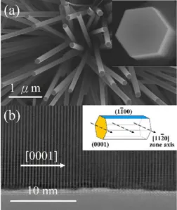
Figure 1. (a) A low magnification SEM image of cylindrical ZnO nanowires. The inset evinces the circular geometry of the nanowire cross-section in a TEM image. (b) High-resolution TEM image of a single cylindrical ZnO nanowire. The inset schematically depicts the zone axis along which direction the TEM electron beam is transmitted into the ZnO nanowire. Planar defects of stacking faults are indicated by triangles.
3. Results and discussion
The as-grown cylindrical ZnO nanowires, mostly lying on substrate surfaces, are depicted in the SEM image of figure1(a). Their dimensions are several microns in length and ∼113 nm in diameter with 18% standard deviation. A slightly bending feature along the nanowire growth direction can be discerned and the Au-nanoparticle catalysts were found to be always bound on one end of the nanowires. In order to confirm their cylindrical geometry, two specimens with nanowires on surfaces were glued together face-to-face and then sliced for TEM image observation of the nanowire cross-section, as depicted in the inset of figure 1(a). A high-resolution TEM image of a single crystalline nanowire is shown in figure 1(b) with 0.52 nm spaced (001) planes, the [0001] growth direction, and some planar defects of stacking faults as indicated. The stacking faults and low angle grain boundaries resulted in the bending nature of the as-grown cylindrical nanowires. We notice that the surface morphology of those cylindrical ZnO nanowires is usually bumpy on a nanometre scale, as is seen in figure1(b), where the inset denotes the zone axis in the TEM experimental configuration.
Structural characterizations of hexagonal ZnO nanowires are shown in figure 2. Unlike cylindrical nanowires, most of the hexagonal nanowires grew straight and preferred vertical alignment on the substrate surface, with an average diameter of ∼134 nm. However, the hexagonal nanowires actually exhibited a very large distribution in diameter, ranging from ∼10 to above 200 nm. A regular hexagon on one end of a hexagonal nanowire is shown in the inset of figure2(a). Although the single-crystalline attribute, lattice spacing and the growth direction are the same as those of cylindrical ones, the hexagonal nanowires possess many fewer stacking New Journal of Physics 10 (2008) 033017 (http://www.njp.org/)
Figure 2. (a) A typical SEM image of hexagonal ZnO nanowires. The inset shows a high magnification SEM image of the hexagonal cross-section of a nanowire. (b) High-resolution TEM image of a single hexagonal nanowire. The inset schematically depicts the zone axis along which direction the electron beam is transmitted into the ZnO nanowire.
faults and, meanwhile, exhibit atomic smoothness of surface morphology on (110) edge planes, as is imaged in figure2(b) and sketched in the inset.
By using TEM, we have directly determined only the planar defects, but not the point defects, in individual ZnO nanowires. Point defects, like ZnI and VO, in this material are by
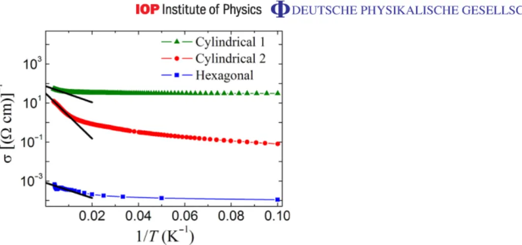
no means easily detectable in the standard electron microscopy studies [27]. Other techniques, namely, electrical conductivity and PL measurements, are thus utilized to investigate the nature of point defects in our ZnO nanowires. Single cylindrical and hexagonal nanowires were dispersed, positioned and patterned to perform four-probe resistance measurements and the temperature behavior of the intrinsic conductivities, σ, was studied. We remark that two-probe electrical characterizations of our ZnO nanowires have been reported [29]. Figure 3 shows σ as a function of the inverse temperature for two cylindrical and one hexagonal nanowire as indicated. We found that the conductivities in hexagonal nanowires are typically 3–6 orders of magnitude lower than those in cylindrical nanowires. The measured low values of conductivity conform to many fewer planar defects, and reveal a lower density of point defects as well as electron donors in the hexagonal ZnO nanowires. Usually, the conductivity varies with temperature T through the temperature-dependent electron concentration and mobility. Assuming weak temperature dependences for the electron mobility [12] and for the effective density of states in the conduction band near room temperature, we obtained the donor activation energy 1ED by comparing the experimental data with the relation σ ∝ exp(−1ED/2kBT),
where kB is the Boltzmann constant. The donor activation energies thus obtained for the
Cylindrical 1, Cylindrical 2 and Hexagonal nanowires shown in figure 3 are ≈20, 40 and 20 meV, respectively. We should stress that, while it is certain that shape effect can dramatically modify the concentration of point defects in cylindrical and hexagonal ZnO nanowires, a full understanding of the origins of the measured activation energies in these undoped materials
6
Figure 3. Inverse temperature behavior of logarithmic conductivity σ for as-grown cylindrical and hexagonal ZnO nanowires as indicated. The diameters of the Cylindrical 1, Cylindrical 2, and Hexagonal nanowires are approximately 87, 125 and 210 nm, respectively. The solid lines are theoretical fits for evaluations of donor activation energies (see text). Notice that the conductivity in the Hexagonal nanowire is considerably lower than in the Cylindrical nanowires.
still requires further studies. The weak decrease inσ with decreasing temperature below about 200 K in the Cylindrical 1 nanowire can be ascribed to the increased electron mobility in this temperature regime [15].
Since the physical properties of ZnO strongly depend on growth conditions, we employ PL spectrum measurements as a second tool to probe the quality of the as-grown nanowires. Figure 4(a) demonstrates distinct PL spectra for cylindrical and hexagonal ZnO nanowires. In order to scrutinize the green defect emission at ∼2.5 eV, the peaks of the near band edge emission at ∼3.2 eV in the two spectra were normalized to the same value. The very prominent green emission intensity undoubtedly indicates surpassing levels of defect concentration in the as-grown cylindrical nanowires. In connection with our observations of high conductivities (figure3) and numerous stacking faults (figure1) in cylindrical nanowires, we argue that these high levels of point defects must be closely associated with the shallow donors that facilitate electrical transport as well as with the planar defects of stacking faults that are sensitive to high-resolution TEM analysis. A shift in the near band emission peak in PL spectra from 3.23 eV for cylindrical nanowires to 3.18 eV for hexagonal nanowires is seen in figure4(a). The PL spectra seems to be in line with room-temperature PL results presented in [30], in which a blue shift in UV emission as well as an intensified green defect emission for ZnO bulk as compared with nanocrystals were shown. This peak shift could possibly stem from either the detection angle dependence [31], the shape effect, the ionized donor–exciton complex [32], or the structural defect induced strain effect [33].
In order to investigate the shape effect on magnetism, the as-grown ZnO nanowires were implanted by high-energy Co ions and then thermally treated in a high vacuum. PL spectra of high-vacuum annealed Zn0.89Co0.11O nanowires with cylindrical and hexagonal
geometries are shown in figure 4(b). We first notice that the PL spectra for as-implanted Zn0.89Co0.11O nanowires also displayed essentially similar behavior, except with a ∼10% higher
intensity at the green defect emission (not shown). High stacking-fault densities in as-implanted nanowires as well as the removal of planar defects together with a recovery of crystalline
Figure 4.Room temperature PL spectra in arbitrary units for (a) as-grown ZnO nanowires and (b) high-vacuum annealed Zn0.89Co0.11O nanowires with circular
and hexagonal cross-sectional geometries.
structure by thermal annealing have previously been observed in Zn1−xCoxO nanowires [23].
Intriguingly, with reference to the normalized peak intensity at near band emission, the high-vacuum annealed Zn0.89Co0.11O nanowires evince a greatly intensified green defect emission
(figure4(b)), as compared with that of the as-grown ZnO nanowires (figure4(a)). In addition, we found that the cylindrical Zn0.89Co0.11O nanowires reveal a blue shift in near band emission and
a stronger green defect emission than in hexagonal Zn0.89Co0.11O nanowires. Unlike in the case
of Ni-doped ZnO nanowires [34], where a red shift at near band emission peak relative to that in pure ZnO was reported, we do not find any change in the peak position between figures4(a) and (b), suggesting no band edge bending in our high-vacuum annealed Zn0.89Co0.11O nanowires. On
the other hand, we observe a red shift of the green defect emission in the high-vacuum annealed Zn0.89Co0.11O nanowires relative to that in the as-grown ZnO nanowires. This latter red shift
seems to be in line with the emission shift from green to yellow found in those nanowires grown under reduced Zn pressure [19].
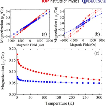
Magnetic properties of as-implanted Zn0.89Co0.11O nanowires were inspected by
performing hysteresis loop measurements at 2 K (see figure5(a)). The as-implanted nanowires barely display any hysteresis loops. Besides, the magnetizations of cylindrical nanowires exceed in magnitude those of hexagonal ones. After high-vacuum annealing, the relative magnitudes of magnetization for the cylindrical and hexagonal Zn0.89Co0.11O nanowires are unchanged,
while the cylindrical nanowires reveal evident hysteresis loops indicating marked ferromagnetic ordering (see figure 5(b)). Taken together with the fact that the green defect emission in PL spectra in the Zn0.89Co0.11O nanowires slightly weakened after annealing, we conclude
that high-vacuum annealing removed planar defects and induced ferromagnetic exchange interaction in those nanowires. This result confirms our previous observation of structure effect on ferromagnetism in Zn1−xCoxO nanowires [35]. Moreover, the stronger ferromagnetic
ordering (figure5(b)), together with the higher green defect emission (figure4(b)), in cylindrical nanowires further supports our previous assertion of enhanced ferromagnetism in Zn1−xCoxO
nanowires by either ZnI or VO [23, 36] which might be created through vacuum annealing.
Figure5(c) demonstrates the temperature behavior of magnetization in Zn0.89Co0.11O nanowires,
where much larger magnetization in cylindrical than in hexagonal nanowires is evident. The magnetization of cylindrical nanowires progressively increases with decreasing temperature,
8
Figure 5. Field dependent magnetization of (a) as-implanted and (b) high-vacuum annealed Zn0.89Co0.11O nanowires measured at 2 K. (c) Magnetization
as a function of temperature measured in a magnetic field of 500 Oe. The red circles and blue squares represent Zn0.89Co0.11O nanowires with cylindrical and
hexagonal geometries, respectively.
implying much stronger ferromagnetic interactions at low temperatures. It should also be emphasized that we have previously excluded any existence of Co clusters in our Zn1−xCoxO
(x 6 0.11) nanowires [23,35,36].
4. Summary
In summary, ZnO and Zn1−xCoxO nanowires of comparable size, and cylindrical and hexagonal
geometries have been fabricated for physical property characterizations. The cross-sectional shape effects on modulations of physical properties in those quasi-1D nanowires have been firmly established. SEM and TEM studies indicate that stacking faults and bumpy edge surfaces are more likely to appear in cylindrical than in hexagonal ZnO nanowires. The as-grown cylindrical nanowires exhibit much higher intrinsic conductivities (as determined from four-point resistance measurements) and intensified green emission in PL spectra. After Co-ion implantation, we have observed larger magnetization and more profound hysteresis loops as well as stronger ferromagnetic ordering in cylindrical than in hexagonal Zn1−xCoxO nanowires.
In particular, the detrimental (beneficial) roles played by the planar (point) defects on the occurrence of ferromagnetism in Zn1−xCoxO nanowires have been established from structural,
electrical, optical and magnetic studies. The present work provides a fairly complete and coherent picture of the shape effect in ZnO-based nanowire materials.
Acknowledgment
This work was supported by the Taiwan National Science Council under grant nos. NSC 94-2112-M-009-020, NSC 94-2120-M-009-010 and NSC 95-2120-M-009-002, and by the MOE ATU Program. The magnetization measurements were performed on a SQUID magnetometer (MPMS XL-7) at the National Chiao Tung University.
References
[1] Duan X, Huang Y, Cui Y, Wang J and Lieber C M 2001 Nature409 66
[2] Cui Y and Lieber C M 2001 Science291 851
[3] Postma H W Ch, Teepen T, Yao Z, Grifoni M and Dekker C 2001 Science293 76
[4] Derycke V, Martel R, Appenzeller J and Avouris Ph 2001 Nano Lett.1 453
[5] Lieber C M and Wang Z L 2007 MRS Bull. 32 99 [6] Wang Z L 2000 J. Phys. Chem. B104 1153
[7] Hu J, Li L S, Yang W, Manna L, Wang L W and Allivisatos A P 2001 Science292 2060
[8] Wang W Z, Poudel B, Ma Y and Ren Z F 2006 J. Phys. Chem. B110 25702
[9] Bagnall D M, Chen Y F, Zhu Z, Yao T, Koyama S, Shen M Y and Goto T 1997 Appl. Phys. Lett.70 2230
[10] Heo Y W, Park S J, Ip K, Pearton S J and Norton D P 2003 Appl. Phys. Lett.83 1128
[11] Look D C and Claflin B 2004 Phys. Status Solidi B241 624
[12] Look D C, Hemsky J W and Sizelove J R 1999 Phys. Rev. Lett.82 2552
[13] Van der Walle C G 2000 Phys. Rev. Lett.85 1012
[14] Cox S F J et al 2001 Phys. Rev. Lett.86 2601
[15] Look D C, Farlow G C, Reunchan P, Limpijumnong S, Zhang S B and Nordlund K 2005 Phys. Rev. Lett.
95 225502
[16] Lany S and Zunger A 2007 Phys. Rev. Lett.98 045501
[17] Vanheusden K, Warren W L, Seager C H, Tallant D R, Voigt J A and Gnade B E 1996 J. Appl. Phys.79 7983
[18] Djuriˇsi´c A B, Leung Y H, Tam K H, Ding L, Ge W K, Chen H Y and Gwo S 2006 Appl. Phys. Lett. 88 103107
[19] Heo Y W, Norton D P and Pearton S J 2005 J. Appl. Phys.98 073502
[20] Dietl T, Ohno H, Matsukura F, Cibert J and Ferrand D 2000 Science287 1019
[21] Ueda K, Tabata H and Kawai T 2001 Appl. Phys. Lett.79 988
[22] Kittilstved K R, Schwartz D A, Tuan A C, Heald S M, Chambers S A and Gamelin D R 2006 Phys. Rev. Lett.
97 037203
[23] Wu Z Y, Chen F R, Kai J J, Jian W B and Lin J J 2006 Nanotechnology17 5511
[24] Coey J M D, Venkatesan M and Fitzgerald C B 2005 Nat. Mater.4 173
[25] Huang M H, Wu Y, Feick H, Tran N, Weber E and Yang P 2001 Adv. Mater.13 113
[26] Yao B D, Chan Y F and Wang N 2002 Appl. Phys. Lett.81 757
[27] Ding Y and Wang Z L 2004 J. Phys. Chem. B108 12280
[28] Wang J, An X, Li Q and Egerton R F 2005 Appl. Phys. Lett.86 201911
[29] Lin Y F, Jian W B, Wang C P, Suen Y W, Wu Z Y, Chen F R, Kai J J and Lin J J 2007 Appl. Phys. Lett.
90 223117
[30] Fonoberov V A, Alim K A, Balandin A A, Xiu F and Liu J 2006 Phys. Rev. B73 165317
[31] Wang X, Summers C J and Wang Z L 2004 Nano Lett.4 423
[32] Fonoberov V A and Balandin A A 2004 Appl. Phys. Lett.85 5971
[33] Seo H W, Bae S Y, Park J, Yang H, Park K S and Kim S 2002 J. Chem. Phys.116 9492
[34] He J H, Lao C S, Chen L J, Davidovic D and Wang Z L 2005 J. Am. Chem. Soc.127 16376
[35] Jian W B, Wu Z Y, Huang R T, Chen F R, Kai J J, Wu C Y, Chiang S J, Lan M D and Lin J J 2006 Phys. Rev. B73 233308
[36] Jian W B, Chen I J, Liao T C, Ou Y C, Nien C H, Wu Z Y, Chen F R, Kai J J and Lin J J 2008 J. Nanosci.


![TraditionalMLCalgorithmsmainlytacklethebatchMLCproblem,wheretheinputdataarepresentedinabatch[24,28].Nevertheless,inmanyMLCapplicationssuchase-mailcategorization[22],multi-labelexamplesarriveasastream.Onlineanalysisistherefore dimensionreducermotivatedbyma](data:image/gif;base64,R0lGODlhAQABAIAAAP///wAAACH5BAEAAAAALAAAAAABAAEAAAICRAEAOw==)