24GHz
active retrodirective antenna array
Tzung-Jir H o n g a n d S h y h J o n g C h u n gA 24GHz active Van Ana planar antenna array proposed for inneasing the vehicle radar echo in a vehicle collision avoidance system is designed and demonstrated. The antenna array contains two parallel linear subarrays. Each sub-array is composed of four receiving microstrip antennas, four transmitting microstrip antennas and four transistor amplliers. At the angles of 4" < 0
< 40", except those very close to the specular direction (0 = 03, the measured backscattering field levels of the fabricated array have variations < 3dB and are at least lOdB higher than those of a metal plate of the same size.
Introduction: The Van Atta retrodirective antenna array [l] pos- sesses the advantage that the reradiated fields from all the trans- mitting elements of the array have a coherent phase in the arrival direction of an incident wave, thus yieldmg
a
broad backscattering field pattern. With this advantage, it has been suggested [2] that planar Van Atta arrays be equipped on vehicle bodies to increase the radar echoesin a
vehicle collision avoidance system [3, 41. In this Letter,a
24GHz active Van Atta microstrip antenna array is developed and demonstrated. As shown in Fig. 1, the array con- tains two parallel linear sub-arrays, with each sub-array formed by four active microstrip antenna pairs. Each antenna pair, e.g. pair 1-1: is composed of a receiving antenna (antenna l), a transmit- ting antenna (antenna 13, and a transistor amplifier incorporated in the midway of a microstrip line connecting the two antennas. The transmitting antennas have the same polarisation as the receiving antennas. The signal captured by each receiving antenna is enlarged by the amplier and is then retransmitted by the cor- responding transmitting antenna.amplifier microstrip line
I -1.
Fig. 1 24 GHr active Van Atfa microstrip ontenna array
Pathces 1 to 8 are receiving antennas and patches 1' to 8' are trans- mitting antennas
Design: To create
a
coherent phase at the wave arrival direction, the four transmitting antennas in each sub-array should have inter-element distances the same as thoseof
the receiving anten-nas.
Also, the phase delays in all the antenna pairs, from one receiving antenna, through the amplifier, to the corresponding transmitting antenna, should be the same or have differences equal to multiples of 360". Here, the inter-element distances betweea the receiving (transmitting) antennas in each sub-array were chosen as8.65mm (0.7 ?.), which were the same as that between the two suh- arrays. To reduce the feedback coupling and avoid oscillation, the distance between the nearest-spaced paired antennas (i.e. antennas 4, 4' and antennas 8,
83 was selected as 14.83mm (1.21). The
size of the whole array was measured tohe
85 x 67.5mm2.The microstrip antennas were fabricated
on a
substrate of E, = 2.2 (dielectric constant) and f = 20mil (thickness) and had a geom- etryas
shownin
the insetof
Fig.
20. A narrow microstrip line(0.5mm wide) with impedance Z, = 9252
was inserted into a
square patch of size 3.96 x 3.96mm2 at a position with input impedance equal to 92Q. A quarter-wave microstrip line with impedance Z , = 68Q was thenused
to transform the impedance to Z, = 5052. This design may reduce the step discontinuity radiation and the interaction between the patch and the wide 50 52 input line(1.54mm widej. The measured return loss and H-plane radiation pattern of the fabricated microstrip antenna are shown in Fig. 2a and b, respectively. The return loss was < -20dB at the centre f r e quency of 24.3GHz, with a lOdB bandwidth of 2.7%. The 3dB radiation beamwidth at 24.3GHz was 4 5 " .
23 24 25 26 -401 22 ~~ frequency, GHz a 10, \ 5
J
-10?!-
-15 -20 -60 -60 -40 -10 -15 -20 -60 -60 -40 -20 0 20 40 60 80 angle, deg bm
-20 a 20 angle, deg b . .40
60 80m
Fig. 2 Measured return loss and H-plonc radiation pattern of inset-fed
microstrip antenno a Measured return loss
b H-plane radiation pattern
Z, = 50
n,
ZI = 68n,
Z2 = 92 QThe amplifier was designed using the packaged NF.42484C high electron mobility transistor (HEMT). Since no design data was available above ISGHz, the through-reflect-line W L ) de-embed- ding method was fnst used to measure the scattering parameters of the HEMT from 18 to 30GHz. Discontinuity effects between the transistor terminals and microstrip lines were incorporated in the measurement so that the measured parameters could be directly used in the subsequent circuit design. The amplifier was designed using the commercial tool HP Series
IV.
Fig. 3 illustrates the measured results of the fabricated amplifier. The transistor was biased at Vcs = 4 . 2 V and V,, = 2V (Io = 10mA). At a fre- quency of 24.3GHz, the amplifier gain was -10dB and the return loss was -23dB.22 23 24 25 26
frequency, GHx -30
1
m
Fig. 3 Measured gain (&I) and return loss ( S J J ) q f H E M T amplifier
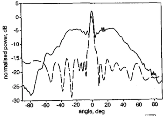
Measurement results: The backscattering field pattern of the fahri- cated active retrodirective array was measured at a distance of 23Om using two closely spaced horn antennas. (The distance was larger than the
far
field distances for the antema array and the measuring horn antennas.) Fig. 4 shows the results at 24.3GHz. As a comparison, the measured backscattering pattern of a metal plate of the same size as the array is also shown. The results were normalised to the backscattering field level of the metal plate at 0". The array scattering pattern showed a narrow peak at 0°, which was due to the strong specular reflection of the array sub- strate ground. With the exception of this peak, the backscattering pattern of the array in the range 4 O-40"
had variation < 3dB and was at least lOdB higher than that of the metal plate.Conduction current crossing domain
boundaries in heterogeneous hybrid
computational electromagnetics formulation
M.A.
Mangoud,
R . A . Abd-Alhameed,P.S.
Excell and
J.A.
VaulA heterogeneous hybid computational electromagnetics method is aresetned that emits conduction currents to aoss the
the two regions. Several validation cases are examined and the mults compared with available data.
Fig. 4 Measured backseatterittr fXd patterns of retrodirective array and metal plate
-
retrodirective array~-~~
metal plateConclusions: A 24GHz active Van Atta antenna array containing eight microstrip antenna pairs has been designed and demon- strated. A transistor amplifer with gain of lOdB was incorporated in each antenna pair to enhance the backscattering field level of the array. With the exception of a high peak in the specular direc- tion, the backscattering field pattern of the array possessed a 3dB beamwidth of 80". Within this beamwidth, the scattering field was at least lOdB higher than that of
a
metal plate of thesame
size. Acknowledgment: This work was supported by the National Science Council of the Republic of China under grant NSC 89- 2213-E-M)9-050.0 IEE 1999
Elecfronics Letters Online No: 19991223 D o l : 10.1049/el:19991223
26 August 1999
Tzung-Jir Hong and Shyh-long Chung (Department of Communication
Engineering, National Chiao Tung University, 1001 T o Hsueh Road, Hsinchu, Taiwan, Republic of Chinn)
E-mail: [email protected]
References
1 VAN ATTA, L.c.: 'Electromagnetic reflector'. US. Patent 2,908,002, Serial no. 514,040, October 1959
2 CHUNG, %I., and CHANO, K.: 'A retrodirective microstrip antenna array', IEEE Trans. Antennas Propag., 1998, 46, (121, pp. 1802- 1809
3 MEINEL, H.H.: 'Commercial applications of millimeterwaves: History, present status, and future trends', IEEE Trans. Microw. Theory Tech., 1995.43, (7), pp. 1639-1653
4 ZELUBOWSKL s.A.: 'Law cost antenna alternatives for automotive radars', Microw. J., 1994, 37, (71, pp. 5&63
~
1786
ELECTRONICS LETTERS
14th October 7999Vol. 35
No. 21 Introduction: Certain problems, notably those involving coupling of a mobile telephone to human tissue, require use of the fnite- difference time-domain (FDTD) method for one part of the proh- lem and the method of moments(MOM)
for another. If conduc- tion current is required to cross the boundary between the two methods, a special treatment is required to ensure current continu- ity across the surface. Earlier work [I ~ 31 is extended for the casewhere the source region is subdivided, one part replaced by equiv- alent surface currents usmg the equivalence principle (computed by MOM) and the other part handled with the use of direct impressed currents (suitable to couple with FDTD). An industry- standard frequencydomain
MOM
programme [4] was used, to aid acceptance in practical applications.Coupling between the scatterer and source regions is calculated using the reaction theorem, with appropriate modifications to the
M O M
program to take account of the fact that the hasis and weighting functions are not the same., ... ;
a b
Fig. 1 Basic geometry of problem a Source and scatterer regions
b Sub-regions A and B of source
c Equivalent surface for currents in sub-region B
C
m
Summary of method: Fig. la shows two regions, one enclosing the source, the other enclosing the scatterer. The source region is fur- ther subdivided into two sub-regions, A and B, as shown in Fig. lb. The scatterer
can
be very close or attached to source region B if it has a dielectric surface. In general, there is no physi- cal attachment between source region A and the scatterer region. The source region was modelled usingMOM
whereas the scatterer was modelled using FDTD. In Fig. 16, the surface S, encloses the entire source region. The fields due to the induced currents from both s o w sub-regions A and B over the closed surface Sclcan
be computed in order to evaluate the surface currents JSi and M,: M s l - n x . - .I ( E ( J A , M A ) + E ( J B , M B ) ) J , ~ = ( H ( J A , M A ) + H ( J B , M B ) ) X A (1) where Ja, JB. MA and MB are the electric and magnetic currents of source regions A and B and