The Design and Assembly of Surface-Micromachined
Optical Switch for Optical Add/Drop Multiplexer
Application
Yu-Chen Lin, Jin-Chern Chiou, Wei-Ting Lin, Yung-Jiun Lin, and Shuen-De Wu
Abstract—An assembly process including: flip-chip bonding, microelectromechanical (MEMS) structure release, and atomic layer deposition (ALD) is proposed to integrate a surface mi-cromachined optical switch for optical add/drop multiplexer (OADM) applications. In the current optical switch designs, pre-stressed beams were used to pop up the micromirror and an electrode (substrate) under the beams was designed to perform ON/OFF function of the optical switch. In order to achieve desired popped-up angle for precise optical switching, a flip-chip bonding technique is applied to a mechanical stopper with an accurate joint height that can be used to constrain the movement of the mi-cromirror. A conformal thin layer of dielectric material(Al2O3) coated on the surfaces of device through an ALD coating process is used to improve vertical actuation force, as well as electrical isolation. Experiments indicate that the micromirrors fabricated by the present assembly process can achieve desired angle that meet the requirements of the proposed OADM configuration.
Index Terms—ALD, flip-chip bonding, micromirror, OADM, optical switch.
I. INTRODUCTION
O
PTICAL switches play an important role in optical com-munication systems. The information exchange is accom-plished by switching and routing optics in the optical networks. To reconfigure the network for preserving the network relia-bility, optical switches are used to bypass failed nodes. Micro-electromechanical system (MEMS) technologies provide a so-lution to manufacture optical switches that enable the cross-con-nect of light signals completely in the optical domain. The ad-vantages of MEMS-based optical switches include high relia-bility, low unit cost/size/weight, low insertion loss, low polar-ization dependent loss, low polarpolar-ization mode dispersion, fast switching time, and wavelength independent [1]–[5].In the dense wavelength division multiplexing (DWDM) networking system, OADM selectively drops a wavelength from a multiplicity of wavelengths in a fiber and adds in the same direction of data flow the same wavelength with different
Manuscript received December 1, 2002; revised June 23, 2003. This work was supported in part by the MTI Center of National Chiao Tung University as well as the National Science Council of R.O.C. under Grant NSC91-2215-E009-028. Y.-C. Lin, J.-C. Chiou, W.-T. Lin, and Y.-J. Lin are with the Department of Electrical and Control Engineering, National Chiao Tung University, HsinChu, Taiwan 300, R.O.C. (e-mail: [email protected]; [email protected]; [email protected]; [email protected]).
S.-D. Wu is with the Precision Instrument Development Center, National Sci-ence Council, HsinChu, Taiwan, R.O.C. (e-mail: [email protected]).
Digital Object Identifier 10.1109/TADVP.2003.817972
data content. As a result, the specific data could be extracted from or carried into the DWDM networking system such that information could be received or transmit among each communication nodes. An OADM configuration that integrated volume holographic gratings with N 2 back-to-back optical switches had been proposed [6]. As illustrated in Fig. 1, the incident lights with different wavelength are coupled into demultiplexer (DMUX) and diffracted into designed position through localized multiplexing method. The optical switches are designed to extract specific information or add the desired one into multiplexer (MUX) by blocking or bypassing the light signals. With this design, the MEMS-based optical switch must have two-states: “OFF” for deflecting the incident lights with micromirror at 45 as well as “ON” for passing incident lights with micromirror at 0 . Note that, the optical switch with 45 popped-up angle brings a great challenge for the requirement of precisely angle control. Mechanical locks [7], [8], actuator platforms [2], [9]–[11] as well as self-assembly by melting the photoresist [12] or by reflowing the solder [13], [14] are the typical methods used to assemble microstructures to reach required position/angle. However, these methods cannot satisfy the required accuracy for the proposed ODAM configuration due to the limitations of fabrication.
In 1996, Toshiyoshi et al. proposed the concept of a mechan-ical stopper [15]. For the developed optmechan-ical switch matrix, the angle of the mirror at ON-state (90 ) is controlled precisely since it touches the stopper on the substrate. In this paper, the concept of mechanical stopper using flip chip packaging technique is proposed and realized to achieve the desired micromirror popped-up angle. Here, the mechanical stopper and mirror were fabricated on two different substrates, and were bonded by using flip chip packaging technology. Precise control of joint height in flip chip bonding guarantees the angle precision of the popped-up mirror. Through this proposed method, the requirement of 45 micromirror popped-up angle for optical switch can be achieved. However, to fabricate a useful optical switch using present configuration, potential problems such as electrical shorting and actuation inefficiency of the pre-stressed beam need to be overcome in advance.
Atomic layer deposition (ALD) for MEMS applications has attracted great interest recently [16], [17]. The fabrication process provides a solution to prevent the electrical shorting and reduce the stiction problem of MEMS structures. Further-more, in the present study, we observed that the actuating force of the pre-stress beams could be greatly enhanced through thermal control of the ALD process. With this extra actuating
Fig. 1. OADM configuration.
Fig. 2. SEM picture of fabricated back-to-back optical switches.
force from the pre-stress beams, we are able to lift the mirror for more than 45 popped-up angle. Thereafter, a mechanical stopper is used to constrain the movement of micromirror to achieve 45 popped up angle.
The paper is organized as follows. Section II introduces the basic concept that combines surface-micromachining with flip-chip packaging techniques to design optical switches for the proposed OADM configuration. Here, flip chip packaging of MEMS is summarized and investigated. The ALD coating process that is used to improve the performance of optical switches is introduced and discussed in Section III. The pre-liminary results of the fabricated optical switches are discussed in Section IV. The angle-control precision of the assembled optical switches is also demonstrated here. The dynamic switching characteristics are used to show the feasibility of the design. Finally, conclusions of the present work are given in Section V.
II. DESIGN OFMEMS-BASEDOPTICALSWITCHES
Fig. 2 shows the SEM of the fabricated optical switches. Electrostatically-driven pre-stressed beams were designed to provide the pop-up forces for the micromirrors. A top-plate is bonded on the top of the pre-stressed beams using flip chip packaging technology to create the mechanical stopper to con-strain the popped-up micromirror to reach required angle. The following sections introduced the design and manufacturing process of the optical switches.
TABLE I
PROCESSFLOW OFFLIPCHIPBONDING
Fig. 3. Joint height versus bonding force of flip chip bonding (with gold bumps at 140 C bonding temperature).
A. Flip Chip Packaging
Flip-chip packaging had been developed and applied to many MEMS designs over the last decade [18]–[20]. It is frequently used to transfer MEMS structures to other substrates that provided MEMS designers a new capability to integrate dif-ferent structures and substrates. A flip-chip packaging process flow developed by CAMPmode, University of Colorado at Boulder, is summarized in Table I [21]. Two designed chips were designed and fabricated in separated substrates. Firstly, solder spheres were deposited on bonding pads using elec-troplating or manual handling. After aligning top and bottom substrates, chips could be bonded together through applying adequate bonding force and bonding temperature. After the release process, which is used to remove sacrificial layer, the MEMS-chips were transferred to the designed substrate plate.
It is known that bonding with solder spheres provides high bonding accuracy due to the re-flowed process for mis-align-adjustment [22]. Solder self-alignment is a predominant technology for electronics assembly and packaging. It is not only used for electrical connections, but also for sub-micron accuracy alignment in many packaging applications [22]–[24]. In addition, a series of work has been done on flip chip bump height control [25], [26]. Here, flip chip bonding with solder spheres and gold bumps were performed to examine corre-sponding reliability and repeatability. Fig. 3 shows an example of the completed flip-chip bonded optical switches with gold bumps. The joint height of the bonding gap is related directly
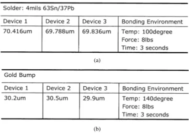
TABLE II
JOINTHEIGHT OFBONDEDPLATESWITHDIFFERENTBONDINGMATERIALS
(a)
(b)
to the bonding forces with the same bonding temperature (140 ). The joint height was recorded for each testing case in the same bonding environment. Table II presents the mea-surement results of joint height for several fabricated optical switches with the same bonding conditions. Three devices were tested for each case. The results showed that the relative errors of the joint height are both within 1%. Experimental results and literature indicated the repeatability in controlling accurate joint height using flip chip bonding is both feasible and reliable. B. Designs and Fabrication
With well-controlled flip chip packaging techniques, the ac-curate bonding gap could be used to control popped-up angle of the mirror. The conceptual design is illustrated in Fig. 4. As stated above, the bonding gap provides the final deflecting angle of the popped-up micromirrors. The relation is given by
(1) where is the bonding gap, is controlled angle, and is the length of the micromirror.
In order to realize the OADM configuration for practical ap-plications, the following difficulties must be put into consider-ations.
1) The material of the mechanical stopper (top-plate): In OADM, the light signals that will be dropped by selected optical switches or those will be added into MUX need to pass so-called “nonblocked” optical paths. To achieve this, transparent materials such as quartz can be used to as the mechanical stopper for the proposed optical switches. However, during the release process of the completed flip-chip bonding chip, the etchant HF will attack quartz substrate that causes roughness on the quartz surface. 2) The bonding gap with accurate joint height: As listed in
(1), we know that the controlled angle is directly re-lated to the bonding gap . This presents a great chal-lenge for flip chip packaging if a larger micromirror size is needed. Using solders with larger diameter could pos-sibly overcome this problem. However, the space of flip
Fig. 4. Conceptual design of the mechanical stopper.
Fig. 5. Layouts of proposed optical switch.
Fig. 6. SEM picture of assembled optical switch.
chip bonding pads that occupied large design space may potentially create the cost and effect problems.
Based on these considerations, a U-shape mechanical stopper is developed to prevent the blockade of the incident light. Fur-thermore, a side panel that is shorter than the length required in (1) is attached to the both sides of the micromirror is designed to reduce the bonding gap without affecting the original de-signed deflecting angle. The layouts of the micromirror and the U-shape mechanical stopper of the optical switch are shown in Fig. 5. Four circular pads at each corner of the micromirror and the stopper were designed for flip-chip bonds. After removing the photoresist, these two designs were aligned and bonded to-gether using the flip-chip bonder developed by CAMPmode, University of Colorado at Boulder [21]. By releasing the sac-rificial PSG layers, the pre-assembly of the back-to-back op-tical switches for proposed OADM configuration was realized. Fig. 6 shows an assembled optical switch. The device was fab-ricated using Cronos/MEMSCAP Poly-MUMPs process [27]. The stopper for flip-chip bonding was fabricated using Poly1 polysilicon layer. The optical switch device consists of a
micro-Fig. 7. Surface profile of the fabricated micromirror.
(a) (b)
Fig. 8. SEM pictures of fabricated optical switches (a) without heat-treatment and (b) with heat-treatment.
mirror (300 in diameter) and four pre-stressed beams (350 in length, 70 in width). Gold (on the top) and Poly2 (on the bottom) layers are chosen as the composite layers of the de-signed pre-stressed beams [28]. An electrode (substrate) under the pre-stressed beams is used to generate electrostatic forces for the purpose of achieving ON/OFF states of the optical switch. The metal layer (Gold) is deposited on the center of mirror to obtain high reflect efficiency ( 80%) [29], [30]. The 0.75- m oxide layer (PSG2) was trapped between two polysilicon layers (Poly1 and Poly2) to reduce warpage of the mirror surface due to residual stress [18]. In Fig. 7, the flatness of surface was mea-sured using Zygo interferometer that shows a 0.5 m difference from center to edge of the mirror surface.
Upon completing flip chip packaging and release process, the micromirrors were assembled by the pre-stressed beams to reach desired angle. However, the unpredictable residual stress induced in the fabrication of pre-stressed beams occasionally did not have enough actuating force to lift the micromirrors to desired angle. This phenomenon can be observed in Fig. 8. Here, optical switches with different pre-stressed beam sizes have been tested. Note that the ones on the left of Fig. 8 did not reach desired angle while the ones on the right did. The substrate was acted as the bottom electrode to actuate pre-stressed beams, which may potentially introduce problem of controlling the N 2 optical switch array individually. This is due to the fact that all the popped-up micromirrors are connected together through the side panels in circuitry that would cause all the mirrors to actuate simultaneously in ON/OFF stage. In order to overcome these difficulties, the ALD coating process was introduced to provide heat-treatment of the pre-stressed beams as well as prevent elec-trical shorting. The process is summarized in Section III.
Fig. 9. Schematic of viscous flow reactor of ALD process [16].
III. ALD COATINGPROCESS
ALD coating technique has gained significant attention in many applications. In 1996, George et al. [31] proposed a bi-nary reaction sequence of self-limiting chemical reactions with one atomic layer deposited during each cycle. The deposition is conformal and creates ultra-thin films with Angstrom-level thickness control. Materials such as dielectric layers ( , , , etc.) or single elements (Si, Ge, Cu, etc.) can be deposited on the surface of corresponding substrates. Recently, ALD coating processes have been applied to MEMS devices to prevent electrical shorting, stiction and mechanical frictional wear of MEMS devices [16], [17]. In this paper, ALD coating process is used to complete the post-assembly of the proposed back-to-back optical switches. By depositing dielectric films, the optical switches can be electrically isolated and the actuation force of pre-stressed beams can be improved effectively. Fig. 9 presents the schematic of the viscous flow reactor developed in University of Colorado at Boulder [21]. Here, is selected to deposit on the pre-assembled back-to-back optical switches. Note that the hard and insulating properties of were ca-pable of preventing mechanical wear and electrical shorting be-tween contacting parts. Note that ALD films are de-posited using alternating trimethyl aluminum (TMA) and exposure. The A and B surface reactions that define an AB cycle (binary reaction) for ALD are [32]
(A) (B) where the asterisks designate the surface species. To perform ALD coating, the chamber is heated and maintained at 177 for required temperature of chemical reaction. At this stage, mi-cromirrors will return to original configuration (parallel to the substrate) due to the characteristics of the pre-stressed beams (gold on top, polysilicon on bottom). By controlling the turn-on time of gas switching valves, the AB cycles of the ALD coating process is performed. Here, a 1000 thickness of dielectric layer was deposited on the fabricated optical switches after a numbers of deposition cycles for electrical isolation. The coated dielectric layer overcomes the previous-mentioned problem such that the designed micromirror can be controlled individually.
In addition, since the temperature of ALD coating process (177 ) is above 110 , the “neutral temperature” of MUMPs chips, the heat-treatment process [28] can be also ac-complished. Once the ALD deposition is finished, the chips can
Fig. 10. Block diagram of proposed assembly process.
be “quenched” by removing the chips from reaction chamber to a cold plate. The heat-treatment process will introduce addi-tional stress into fabricated pre-stressed beams for improving actuating efficiency. With the mechanical stopper on top, the micromirrors are popped-up to reach precise designed angle.
Fig. 10 summarized the proposed assembly process that is given as follows.
1) Soak MUMPs chips 10 15 min in acetone to remove photoresist.
2) Put solder balls or gold bumps on the designed bonding pads.
3) Perform flip chip packaging process to bond top and bottom chips.
4) Soak bonded chips 4 6 min in HF acid to remove sac-rificial layers (PSG).
5) Soak released chips in methanol and performs typical MEMS drying process.
6) Perform ALD coating process to provide electrical isola-tion and heat-treatment of pre-stressed beams.
Once the assembly process is completed, the fabricated optical switches can reach the desired angle according to the bonding gap.
IV. EXPERIMENTS
The popped-up angle of micromirrors during the ON/OFF stage of the applied electrostatic force was under investigation. Fig. 11 illustrates the optical configuration to measure the popped-up angle of the fabricated optical switches. The laser is manually aligned to the popped-up micromirror until the path of incident light coming from laser and reflected light from the micromirror is the identical one. This implies that the popped-up angle of the micromirror is equal to two times of the tilting angle of the rotation mirror . Table III lists the measurement results of the assembly optical switches. In comparison to the proposed 45 popped-up angle for the OADM configuration, the relative error is within 1.6%, which shows the capability of the present assembly process in con-trolling the angle of the micromirrors. Finally, Fig. 12 shows the results of dynamic characteristics of the fabricated optical
Fig. 11. Optical configuration to measure the popped-up angle of optical switch.
Fig. 12. Dynamic characteristic of the fabricated optical switch. TABLE III
MEASUREDPOPPED-UPANGLE OF THEASSEMBLEDOPTICALSWITCHES
switches. The ON/OFF states of the optical switch were tested. The switching speed of the present experiment had reached 100 Hz with 2 ms switching time. The electrostatic pull-down voltage of the pre-stressed beams is about 100 V and the power consumption is estimated to be less than 0.2 mW.
V. CONCLUSION
A surface-micromachined optical switch had been de-veloped for OADM applications through the integration of Cronos/MEMSCAP Poly-MUMPs processing, flip chip pack-aging, and ALD coating. A mechanical stopper was designed to constrain the movement of popped-up micromirrors to reach desired angle. An ALD coating process is applied to enhance the actuating force of the pre-stress beams as well as to ac-complish electrical isolation. Experiments have demonstrated the feasibility of the fabricated optical switch using proposed assembly process.
ACKNOWLEDGMENT
The authors would like to thank Dr. Y. C. Lee’s and Dr. V. M. Bright’s Research Group, Department of Mechanical Engi-neering, University of Colorado at Boulder, for the supports of flip chip packaging and measurement, and Dr. S. M. George’s Research Group, Department of Chemical Engineering, Univer-sity of Colorado at Boulder, for ALD deposition.
REFERENCES
[1] L. Y. Lin, E. Goldstein, and R. W. Tkach, “Free-space micromachined optical switches with sub-millisecond switching time for large-scale op-tical crossconnect,” IEEE Photon. Technol. Lett., vol. 10, pp. 525–527, Apr. 1998.
[2] S. S. Lee, L. S. Huang, C. J. Kim, and M. C. Wu, “Free-space fiber-optics switches based on MEMS vertical torsion mirrors,” IEEE J. Lightwave
Technol., vol. 17, pp. 7–13, Jan. 1999.
[3] R. T. Chen, H. Nguyen, and M. C. Wu, “A low voltage micromachined optical switch by stress-induced bending,” in Proc. 12th IEEE Int. Conf.
Micro Electro Mech. Syst. (MEMS 99), 1999, pp. 424–428.
[4] A. Q. Liu, X. M. Zhang, V. M. Murukeshan, Q. X. Zhang, Q. B. Zou, and S. Uppili, “An optical crossconnect (OXC) using drawbridge micromir-rors,” Sensors Actuators A 97–98, pp. 227–238, 2002.
[5] J. Zhang, Z. Zhang, Y. C. Lee, V. M. Bright, and J.John Neff, “De-sign and investigation of multi-level digitally positioned micromirror for open-loop controlled applications,” Sensors Actuators A 103, pp. 271–283, 2003.
[6] J. C. Chiou, Y. C. Lin, S. D. Wu, and S. H. Lin, “MEMS-based micromirror device for optical add/drop module,” in Proc. SPIE
MICRO/MEMS’01, Adelaide, Australia, 2001, pp. 82–88.
[7] A. Friedberger and R. S. Muller, “Improved surface-micromachined hinges for fold-out structures,” IEEE J. Microelectromech. Syst., vol. 7, pp. 315–319, Mar. 1998.
[8] J. S. Park, L. L. Chu, A. D. Oliver, and Y. B. Gianchandani, “Bent-beam electrothermal actuators—part II: linear and rotary microengines,” IEEE
J. Microelectromech. Syst., vol. 10, pp. 255–262, Feb. 2001.
[9] H. Nguyen, J. Su, H. Toshiyoshi, and M. C. Wu, “Device transplant of optical MEMS for out of plane beam steering,” in Proc. 14th Int. Conf.
Micro Electro Mech. Syst. (MEMS’01), 2001, pp. 325–328.
[10] M. H. Kiang, O. Solgaard, Y. K. Lau, and R. S. Muller, “Electrostatic combdrive-actuated micromirrors for laser-beam scanning and posi-tioning,” IEEE J. Microelectromech. Syst., vol. 7, pp. 27–37, Jan. 1998. [11] R. A. Conant, P. M. Hagelin, U. Krishnamoorthy, M. Hart, O. Solgaard, K. Y. Yau, and R. S. Muller, “A raster scanning full-motion video display using polysilicon micromachined mirrors,” Sensors Actuators A 83, pp. 196–291, 2000.
[12] R. R. A. Syms, “Surface tension powered self-assembly of 3-D micro-optomechanical structures,” IEEE J. Microelectromech. Syst., vol. 8, pp. 448–455, Dec. 1999.
[13] K. F. Harsh, V. M. Bright, and Y. C. Lee, “Solder self-assembly for three-dimensional microelectromechanical systems,” Sensors Actuators A (3), pp. 237–244, 1999.
[14] B. McCarthy, V. M. Bright, and J. A.John A. Neff, “A multi-compo-nent solder self-assembled micromirror,” Sensors Actuators A 103, pp. 187–193, 2003.
[15] H. Toshiyoshi and H. Fujita, “Electrostatic micro torsion mirrors for an optical switch matrix,” J. Microelectromech. Syst., vol. 5, pp. 231–237, Dec. 1996.
[16] N. D. Hoivik, J. W. Elam, R. J. Linderman, V. M. Bright, S. M. George, and Y. C. Lee, “Atomic layer deposited protective coatings for micro-electromechanical systems,” Sensors Actuators A 103, pp. 100–108, 2003.
[17] N. D. Hoivik, J. W. Elam, S. M. George, K. C. Gupta, V. M. Bright, and Y. C. Lee, “Atomic layer deposition (ALD) technology for reliable RF MEMS,” in Proc. IEEE MTT-S 2002 Int. Microwave Symp., Seattle, WA, June 02–07, 2002, pp. 1229–1232.
[18] A. Tuantranont et al., “Self-aligned assembly of microlens arrays with micromirrors,” in Proc. 1999 Int. Soc. Optical Eng. (SPIE ’99), vol. 3878, Santa Clara, CA, 1999, pp. 90–100.
[19] R. Irwin et al., “Quick prototyping of flip chip assembly with MEMS,” in Proc. 1998 IEEE Radio Wireless Conf. (RAWCON ’98), Colorado Springs, CO, Aug. 9–12, 1998, pp. 293–296.
[20] J. C. Chiou, Y. C. Lin, and S. D. Wu, “Closed-loop fuzzy control of torsional micromirror with multiple electrostatic electrodes,” in Proc.
IEEE/LEOS Int. Conf. Optical MEMS, 2002, pp. 85–86.
[21] MEMS. (2003). Tech. Rep., Dept. Mech. Eng., Univ. of Colorado, Boulder, CO. [Online]http://mems.colorado.edu.
[22] A. R. Mickelson, N. R. Basavanhally, and Y. C. Lee, Optoelectronic
Packaging. New York: Wiley, 1997.
[23] T. H. Ju, W. Lin, Y. C. Lee, D. J. McKnight, and K. M. Johnson, “Pack-aging of a 128 by 128 liquid crystal-on-silicon spatial light modulator using self-pulling soldering,” IEEE Photon. Technol. Lett., vol. 7, pp. 1010–1012, Sept. 1995.
[24] T. S. McLaren, S. Y. Kang, W. Zhang, D. Hellman, T. H. Ju, and Y. C. Lee, “Thermosonic flip-chip bonding for an 82 8 VCSEL array,” in
Proc. IEEE 45th Electron. Comp. Technol. Conf., Las Vegas, NV, May
1995, pp. 393–400.
[25] T. S. McLaren, S. Y. Kang, W. Zhang, T. H. Ju, and Y. C. Lee, “Ther-mosonic bonding of an optical transceiver based on an 82 8 vertical cavity surface emitting laser array,” IEEE Trans. Comp., Parts,
Manu-fact. Technol. B, vol. 20, pp. 152–160, May 1997.
[26] W. Lin, S. K. Patra, and Y. C. Lee, “Design of solder joints for self-aligned optoelectronic assemblies,” IEEE Trans. Comp, Packag.,
Man-ufact. Technol. A, vol. 18, pp. 543–551, Aug. 1995.
[27] D. Koester, R. Mahedevan, B. Hardy, and K. Marcus. (2001) MUMPs Design Handbook. [Online]http://www.memsrus.com/
[28] D. C. Muller, W. Zhang, and V. M. Bright, “Microrelay packaging tech-nology using flip-chip assembly,” in Proc. 2000 IEEE Int. Conf.
Micro-electro-Mech. Syst. (MEMS’00), Miyazaki, Japan, Jan. 23–27, 2000, pp.
265–270.
[29] J. Zou, C. Byrne, C. Liu, and D. Brady, “Optical properties of micro-machined polysilicon reflective surfaces with etching holes,” in Proc.
SPIE, vol. 3511, pp. 307–314.
[30] R. Zaouk, “Literature review and preliminary study on feasibility of a MEMS polarization mode dispersion compensator,” Master’s thesis, Univ. of California, Irvine, CA, 2002.
[31] S. M. George, A. W. Ott, and J. W. Klaus, “Surface chemistry for atomic layer growth,” J. Phys. Chem. (100), pp. 13 121–13 131, 1996. [32] A. W. Ott, J. W. Klaus, J. M. Johnson, and S. M. George, “Al O thin
film growth on Si(100) using binary reaction sequence chemistry,” Thin
Solid Films 292, pp. 135–144, 1997.
Yu-Chen Lin received the B.S. and M.S. degrees
in electrical and control engineering from National Chiao Tung University, Taiwan, R.O.C., in 1997 and 1999, respectively, where he is currently pursuing the Ph.D. degree.
His research interests are MEMS design, pack-aging, integration and application.
Jin-Chern Chiou received the M.S. and Ph.D.
de-grees in aerospace engineering science from the Uni-versity of Colorado, Boulder, in 1986 and 1990, re-spectively.
Before joining Department of Electrical and Con-trol Engineering, National Chiao Tung University, Taiwan, R.O.C., in 1992, he worked at the Center for Space Structure and Control, University of Colorado as a Research Associate, from 1991 to 1992. His research interests include micro-electro-mechanical systems (MEMS), fuzzy logic modeling and control of CVD process, servo control of CD-ROM and DVD, and modeling and control of multibody dynamic systems (MBD). He is the co-author of the advanced reference books CD-ROM System Technology and Mechanics and
Control of Large Flexible Structures. He has two U.S. and three R.O.C. patents.
Dr. Chiou received several awards from Acer Foundation, NCTU, and the National Science Council, R.O.C., for his outstanding CD-ROM and MEMS research.
Wei-Ting Lin received the B.S. degree and M.S.
degree in electrophysics from National Chiao Tung University, Taiwan, R.O.C., in 1996 and 1999, respectively, where he is currently pursuing the Ph.D. degree in electrical and control enginering.
His current interests include the design and fabri-cation of microelectromechanical system (MEMS).
Yung-Jiun Lin received the B.S. and M.S. degrees
in auto control engineering from Feng Chia Univer-sity, Taiwan, R.O.C., in 1997 and 1999, respectively, and is currently pursuing the Ph.D. degree in elec-trical and control engineering at National Chiao Tung University, Taiwan.
His research interests focus on MEMS design and application.
Shuen-De Wu received the Ph.D. degree in electrical
and control engineering from National Chiao Tung University, Taiwan, R.O.C., in 1998.
He has worked at Precision Instrument Develop-ment Center, Taiwan, as a Research Associate since 1998. His research interests include control theory and modeling of multi-body dynamic systems.