the clad region of the fibre was fully immersed in turn in a range of pH buffer solutions from a pH of 2 to 8. Fig. 3 shows the fluorescence intensity at i = 530nm, recorded as a func- tion of pH, for a fixed laser emission power of 3 mW. It can be
~- ‘..i 3
P h ~ ~-
Fig. 3 p H sensitivify o f w - g e l sensor
seen that greatest sensitivity to pH change occurs in the region pH 3.5-6.5. The response time of the sensor to a step change in pH was found to be approximately 5 s . This time appears to be governed by the mass transfer of the hydrogen ions through the sol-gel matrix to the fluorescein molecules. Although higher signals could be achieved by increasing the laser power, significant photobleaching of the dye became evident. Finally, no washout of the dye was observed as the fluorescent intensity in water remained constant despite repeated washings.
Conclusion: The use of porous sol-gel glass as a support struc- ture for chemically-sensitive dyes in evanescent-wave optical waveguide sensors has been demonstrated. The low tem- perature of the process enables use of a wide range of dyes of low thermal stability. This novel technique is particularly suited to gas sensing where the high specific area of the con- tinuous porous structure is particularly important. In addi- tion, it olfers the potential for fully distributed or quasidistributed multipoint sensing. This could be achieved by coating a fibre along its total length during drawing or by splicing in sensing regions. Where simple point sensing is required, it is a relatively straightforward process to coat the endface of a fully clad fibre. Finally, the compatibility of the sol-gel coating with the silica substrate makes the technique particularly suitable for planar waveguide sensors formed by ion exchange in glass.
B. D. MAcCRAITH 22nd March / Y Y I
V. RUDDY C. POTTER
School of Physical Sciences Duhlin City Uniaersity Glasnevin, Dublin 9. Ireland B. O ‘ K E L L Y
J. F. McGILP
Department of Pure and Applied Physics Dublin Unrrersity
Trinity College Dublin 2. Ireland References
1 NOKKIS, J. 0. w.: ‘Current status and prospects lor the use of optical fibres in chemical analysis- -a review’, Analyst, 19x9, 114, pp. 1359-1372
LIEBERMAN, R. A., BLYLER. L. L., and T O W N . L. G . : ‘A distributed 2
fiber-optic sensor based on cladding flurorescence‘. J. Lightwave Technol., 1990,8, (2). pp. 212-220
WOLPB’CIS, 0. s.: ‘Fibre optical fluorosensors in analytical and clini- cal chemistry’. in SCHULMAN, s. J. (Ed.): ‘Molecular luminescence
spectroscopy-Part II’ (John Wiley & Sons, New York, 19XX), pp. 129-281
MUKHERJEE, S. I,.: ‘%-gel processes In glass Sclence and tech-
nology’, .I.Non-Crysf. Solids, 1980.42, pp. 4 7 7 ~ 488
WANG, F . : ‘Single fibre optic fluorescence pH probe’, A n a l p t . 19x7, 112, pp. 1159-1 I63
3
4
5 FIJH, M. S., BIIRGFSS, L. W., HIRSCHFELO, T., THRISTIAU, Ci U,, and
1248
B i C M O S EDGE DETECTOR W I T H READOUT CIRCUIT FOR PATTERN RECOG NlTlON NEURAL NETWORK CORRELATED-DOUBLE-SAMPLING
Indexing terms: Detectors and detector circuits, Image pro- cessina. Neural networks
A new image sensor is presented that comprises a chopper- stabilised edge detector and a correlated-double-sampling readout circuit, based on 2pm BiCMOS technology for pattern recognition neural network VLSI applications oper- ating at 77 K . With the chopper-stabilised edge detector and the correlated-double-sampling readout technique, the two- dimensional photodiode array, which can be elliciently built with only one readout circuit, provides a bidirectional edge detection capability for high resolution image sensing appli- cations operating at 77 K.
I n t r o d u c i i o n . Recently, pattern recognition implemented by the neural network techniques has been the major method for machine vision applications. Usually, the image of the object is recorded by a 2-D photodetector array such as charge- coupled device (CCD), followed by the edge detection of the object; the recognition function is then performed. A ‘smart’ edge detector resembling the response of a biological retina, which is made of over 30 transistors and one phototransistor
as a pixel unit and can be used to extract the edge position of an object image, has been realised using CMOS analogue VLSI circuit techniques.’ A simpler ‘on-centre’ edge detector composed of two back-to-back-connected concentric or direc- tional photodiodes realised by amorphous silicon technology has also been reported.’ The generated edge signal, which can be either positive or negative, is proportional to the difference of the two photocurrents associated with two photodiodes if the edge of the image happens to fall on the detector. In this Letter, a new image sensor using two pairs of cross-coupled BiCMOS photodiodes with chopper-stabilised switches and a correlated-double-sampling readout circuit operating at 77 K for bidirectional edge detection, is described.
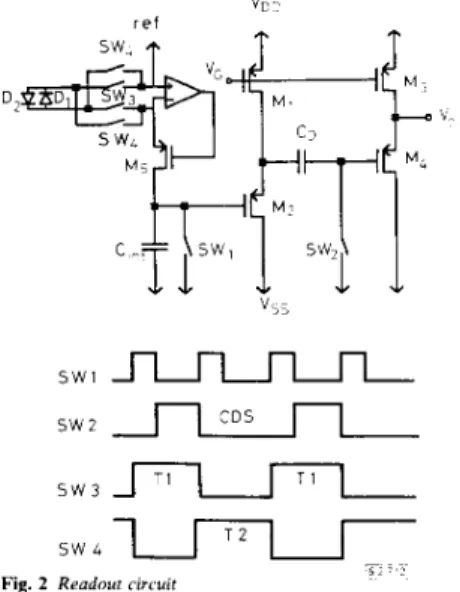
Edge detector cirruit . This new image-sensor is composed of a n edge detector array and a readout circuit. As shown in Fig.
1 in each pixel area, two cross-coupled pairs of back-to-back- connected photodiodes can be used to perform bidirectional edge detection. Compared with traditional image sensors such
word hne D: 0 2 ____ bitlhe D ?
162111
Fig. 1 Cross-coupled pairs oJ back-to-buck-connected photodiodes in each pixel ureaas CCDs, in the edge detector each pair of photodiodes gener- ates a nonzero net current only when an image edge falls on the detector. This arrangement facilitates an efficient recording of the edge information of an image. The readout circuit com- prises a word-line decoder, a bit-line decoder, and a current integrator/output buKer. As in SRAM memory cells, together with the word-line and bit-line decoder outputs, four-pass transistors using chopper-stabilised techniques’ are used to provide access to the current integrator/output buffer for each individual pair of the photodiodes as shown in Fig. 2. In addition, the chopper-stabilised switches also facilitate bidirec- tional edge detection as a result of the nonzero net current coming from the photodiode pair. Consequently, a two- dimensional edge detector array can be constructed with the basic edge detector cell, which is composed of two cross- coupled pairs of hack-to-back-connected photodiodes and eight switches. Furthermore, only one readout circuit is neces- sary for the whole edge detector array and the effective area in
image sensing can he raised owing to the drastic reduction of the nonphotodiode area. As shown in Fig. 2. the current
b-. Fig. 2 S W I SW 2 CDS 5 w 3
l 7 - J - l
i tI
T 2 ~ ~~ s w L Readout circuit 6 2 ' 2integrator/output buffer, which is used to convert the photo- current into an output voltage signal for further processing is made of an opamp, an integrating capacitor C,,,, a reset switch SWI, and a feedback PMOS transistor to ensure a zero-biased operation for the accessed photodiodes at an opti- mised efficiency. Two PMOS source followers with a capacitor C,, and a switch SW2 are used as an output buffer with a correlated-double-sampling mechanism" to reduce noise effects and t o facilitate recording of the nonzero net current from the photodiodes with clock timing as shown. During T1, SW3s are on and the selected photodiodes are connected to the readout circuit. As SWl is high, the integrating capacitor C,,,, is grounded and capacitor C, is floating. As SW2 turns on and SWI is off, integrating capacitor C,,, is charged by the photocurrent generated by the accessed photodiodes, and the right plate of the capacitor C , is grounded. At the end of the T1 period, the capacitor C , contains the sampled reset noise and the charge associated with the photocurrent of the same photodiodes biased at a polarity set by SW3s. During T2, the polarity of the selected photodiodes is reversed and SW2 is always off. As S W l turns off, the charge corresponding to the photocurrent of the same photodiodes with the polarity reversed by turning on SW4s is coupled to capacitor C,. The difference in charge associated with capacitor C , between TI and T 2 shows up in the output voltage
Ku,
at the end of the T 2 period. Incorporating the modified correlated-double-sam- pling mechanism, the new detector circuit not only can detect a positive or negative photocurrent hut also can reduce the thermal and flicker noise effects generated in the analogue front end of the readout circuit.C i r c u i t p e r f o r m a n c e : CMOS analogue circuits operating at 7 7 K o f e r low noise advantages,' which are particularly important for high performance image sensing circults.6 Cur- rently, SPICE device models are not sufficient for simulation of circuits operating at 77 K. T o design the image sensor oper- ating at 77 K , low temperature SPICE models have been suc- cessfully developed. With appropriate low temperature models, a CMOS two-stage opamp with a DC gain of over 1o00, and a unity gain bandwidth of 2 M H z has been designed. Overall transient behaviour of the image sensing circuit operating at 77 K is shown in Fig. 3.
In a pixel area, with photodiode D2 illuminated by a light source and the other photodiode, D1. masked, the output voltage Vou, actually shows a larger value at the end of T2 as compared to that at the end of T1. On the other hand, with D2 masked and D1 illuminated, a smaller output voltage at the end of T2 can he seen. Experimental low temperature
ELECTRONICS LETTERS 4th July 1997 Vol. 27 No. 14
results contirm the simulation results as shown. Thus, the bidirectional edge detection capability of the new image sensing circuit using a chopper-stabilised edge detector and a correlated-double-sampling readout circuit has been verified. Fig. 4 shows the layout of the 2 x 2 image sensing circuit based on 2 p m BiCMOS technology. Digital hit-line and word-line decoder circuits are shown in the upper and central portions of the tigure. The centre-right portion is the edge detector array and at lower right is the opamp related readout circuit. Total chip area is around 1400pm x 1200pm.
4 ; : : ~ -
,n
1
$
o 2 0 v 0 L O 80 120 1 6 C Z G G 2 4 0 2 8 C 3 2 02
1 ovV m f o r T1 t i m e , u s
m
cycle integmting
Fig. 3 Orerall transient behaviour if image sensing circuit operating at
??K
~~~~ temperature = 25.0 C
____ temperature = - 196-0 C
Fig. 4 Layout of image sensrng circuit
Conclusion: In conclusion, with the chopper-stabilised edge detector and the correlated-double-sampling readout circuit, the new sensing circuit can provide an SRAM-type two- dimensional expansion capability in implementing pattern recognition VLSI for bidirectional edge detection at 77 K . I. B. K U O
T L. CHOU E. I. WONG R m . 526
Department of Electrical Engineering Narionol Taiwan Dniuersitj' Ronsevelr Rd.
Sec 4 , 7'uipei IO?, T a w a n , Repuhlk oJChina References
1 2
22nd April 1991
M ~ A U , r.. 'Analog VLSI and neural systems' (Addison Wesley,
1989)
FAH, w. J.. LEE, s. c., and CHEN. J. H ' 'Amorphous silicon edge
detector for application lo electronic eyes'. IEEE Dig. of h i . Elec-
tron Device Meeting, December 1989, pp. 515-518
____ I , 3 4 5 6
HSIEH, K. c., GRAY, P. R., SENDEROWICZ, o., and M E S S E R S C H M I ~ , D.
G.: ‘A low-noise chopper-stabilized switched-capacitor filtering technique’, IEEE J. Solid-Srare Circuirs, 1981, SC-16, (6), pp. 708-715
KANSY, R. J . : ‘Response of a correlated double sampling circuit to
ljf noise’, IEEE J. Solid-State Circuits, 1980, SC-15, ( 3 ) . pp. 373-37s
FOX, R. M., and JAEGER, R. c . : ‘MOSFET behavior and circuit con-
sideration for analog applications at 77K‘, IEEE Trans., 1987, ED-34,(1), pp. 114123
SCHOENEBER, U,, HOSTICKA, B. I., ENT, I., OBERLACK, H., and ZIMMER, G.: ‘CMOS readout electronics for operating at cryogenic tem- peratures’, IEEE J. Solid-State Circuits, 1989, SC-24, (3). pp. 718-722
adjacent channel interference. From the baseline performance measurements, it can be seen that SSB performs significantly
20 181 C16
FIELD TRIAL EVALUATION OF LINEAR MODULATION SINGLE SIDEBAND
Indexing rerms: Radiocommunication, Mobile radio sysrems A series of field trials to assess the performance of a VHF trunked PMR system using 5kHz bandwidth linear modula- tion single sideband technology compared with existing 12.5 kHz FM and AM systems are described. Relative per- formance figures are given.
I n t r o d u c t i o n : With the ever increasing use of private mobile radio (PMR) and cellular systems, spectrum congestion is becoming a pressing problem. One possible step towards effec- tive spectrum use is the introduction of narrowband systems, such as 5 k H z channel spaced linear modulation single side- band (LM-SSB). T o provide information on the effects of such an introduction, the DTI Radiocommunications Agency com- missioned Bradford University to carry out a series of inde- pendent field trials to compare the performance of 5 k H z LM-SSB with 12.5 kHz F M and AM, operating between 165 and 170MHz. The LM-SSB system under test was a proto- type model using the transparent tone in band (TTIB) tech- nique developed at Bristol University.’ This prototype model was compared with a Tait T377 F M system with two T530 mobiles and a Pye T401 AM system with M201 mobiles. Field trial i m p l e m e n t a t i o n : Measurements were made for transmissions from a base station t o a mobile following a carefully defined route at a constant 30mph. Each base station was calibrated to give equal average incident field strength. Both voice and data measurements were taken for all three modulation schemes without interference, and a subset of these experiments was then repeated with various single, voice-modulated, adjacent or cochannel interferers. The channel separation for adjacent channel tests was 5 kHz for two SSB channels, and IOkHz for other cases. The results given here are for a composite route made up of individual sections with average signal strength ranging from 52 dBpV to under OdBpV and widely varying fading depths. The only exception to this is the cochannel results which are carried out on a single route of signal strength between 10dBpV and 36dBpV and fading greater than 10dB. The methods of assessment used were as follows:
(I) The speech intelligibility of the systems was investigated using the diagnostic rhyme test (DRT),’ which uses a panel of listeners to produce a score for average percentage unintelligi- bility. Listeners also scored each entire test on a five point scale, to include some element of subjective quality assess- ment.
(2) The bit error rate (BER) was used as a measure of the ability of the systems t o transmit data. V23, V27bis and V29 modems were used t o measure the BER for data rates between 1.2 Kbit/s and 9.6 Kbit/s.
V o i c e r e s u l t s : Fig. I shows the percentage unintelligibility scores for SSB, FM and AM with no interference and with 1250
modulation type
Fig. I Voice results with adjacent channel interference Composite route
0 baseline SSB interference FM interference AM interference
better than either F M or AM. However, despite its high objec- tive intelligibility, SSB proved unpopular with listeners, who found its tone unpleasant.
In terms of interference, SSB is highly resistant to both SSB and F M adjacent channel interference. However, AM inter- ference has a significant effect on SSB, and this is likely to be the limiting factor in the integration of SSB with an existing spectral environment. It is interesting t o note that LM-SSB with any form of interference performs better than baseline F M or AM.
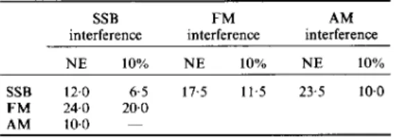
As previously stated, cochannel measurements were taken for each system on one sample route (rather than the compos- ite route). Two protection ratios, of 2 d B and 8 dB, were used, and with the results obtained, estimates for the required pro- tection ratios for two different scenarios were made for each of the channel configurations tested.
!l) T F value of protection ratio required to obtain a DRT intelligibility score identical t o the relevant baseline measure- ment was calculated. This is the protection ratio required for the interferer to have no noticeable effect on the speech intelli- gibility.
(2) Also calculated was the value of protection ratio required t o given a chosen DRT figure of 10% unintelligibility, assessed by the listeners as ‘tolerable’.
For both of these protection ratio figures, a linear relationship between the intelligibility and protection ratio is assumed. Table 1 shows the calculated protection ratios. It can be seen Table 1 ESTIMATED PROTECTION RATIOS FOR
VOICE WITH COCHANNEL INTERFERENCE
SSB F M AM
interference interference interference
N E 10% N E 10% N E 10%
SSB 12.0 6.5 17.5 11.5 23.5 10.0
F M 24.0 20.0
AM 10.0 ~
NE: Protection ratio for no effect on intelligibility lo%,: Protection ratio for 10% unintelligibility
that F M is extremely susceptible to SSB cochannel inter- ference but that AM is fairly resistant. SSB is highly resistant t o SSB interference, less so to F M interference and is badly affected by AM. However, the 10% protection ratios for all these positions are low because of the good absolute intelligi- bility of SSB.
Data r e s u l t s : Fig. 2 shows the number of errors per million bits for the three modulation schemes; a variety of bit rates using various baseband modems are used for SSB and FM, but not for AM. This figure shows the difficulty that this implementation of LM-SSB has in coping with data rates above 2.4 Kbit/s using standard line modems. Fig. 3 shows the effects of voice modulated adjacent channel interference on 1.2Kbit/s data transmission. In all cases, the effect is much ELECTRONICS LETTERS 4th July 1991 Vol. 27 NO. 14