0040-6090/02/$ - see front matter䊚 2002 Elsevier Science B.V. All rights reserved. PII: S 0 0 4 0 - 6 0 9 0 Ž 0 2 . 0 0 7 4 9 - 6
Iron and cobalt silicide catalysts-assisted carbon nanostructures on the
patterned Si substrates
Hui Lin Chang*, Chao Hsun Lin, Cheng Tzu Kuo
Department of Material Science and Engineering, National Chiao Tung University, Hsinchu 300, Taiwan, ROC
Abstract
Catalyst-assisted carbon nanotubes(CNTs) and carbon nano-rods were synthesized on the patterned or un-patterned Si wafer by microwave plasma chemical vapor deposition, using iron or cobalt silicide catalysts. Controllable carbon nanostructures were achieved by manipulating carbon and nitrogen concentration in the source gases, catalyst materials, and patterned wafer application. CNTs were synthesized under a high ratio of CH4yH s0.1, while carbon nano-rods were synthesized under a low ratio of CH y2 4
H s0.01. Introducing N gas into CH2 2 4yH source gases gives rise to bamboo-like CNTs formation. Selective CNTs depositions2
were applied on(a) parallel Fe-coated line arrays, (b) CoSi -coated hole arrays. This is a novel method that is compatible withx Si microelectronic device manufacturing. The field emission results indicate that the emission current density can be above 1 mAycm at 3.97 Vymm, and hollow like CNTs belong to better emission current than bamboo-like CNTs. Growth models of2
different carbon nanostructures are proposed. 䊚 2002 Elsevier Science B.V. All rights reserved.
Keywords: Carbon; Field emission; Chemical vapor deposition; Catalysis
1. Introduction
Carbon nanotubes (CNTs) that consist of sheet(s) of graphite (a hexagonal lattice of carbon) rolled into a cylinder, were discovered in 1991 by Iijima w1x. This novel material has inspired much excitement in recent years and a large amount of research has been dedicated to their understanding. Mechanically, the axial Young’s modulus of multi-walled CNTs can be as high as 1800 GPa, and the tubes can thus be much stiffer than commercial carbon fibers w2x. Electrically, the tubes are either metallic or semiconducting depending on their chirality w3,4x. Chemically, the tubes are inert and highly resistant to oxidation w5x. The unique properties of CNTs are also predicted to possess a great potential in appli-cations of scanning probes w6x, field emission (FE) display w7x, anode for lithium ion batteries w8x, nano-electronic devices w9x, supercapacitors w10x, molecular sensors w11x and hydrogen storages w12x.
The goals of CNTs synthesis can be considered to be CNTs with highly ordered orientations, fewer defects and reproducibly controllable properties. Chemical vapor
*Corresponding author. Tel.: 5739845; fax: q886-3-5724727.
E-mail address: [email protected](H.L. Chang).
deposition (CVD) method offers advantages of control-ling CNT orientations and properties, by varying syn-thesis parameters and substrate pretreatment. For example, an enhanced CVD approach can obtain direc-tionally suspended SWNTs networks in which the SWNTs are aligned and parallel to the substrate w13x. Also, CVD methods can be used to obtain various kinds of CNTs, such as CNTs with a perfect Y-junction or straight line, bridging CNTs on two parallel patterned structures, the selective, lateral growth of bamboo-like CNTs w14,15x.
This study systematically explores the carbon nano-structures synthesized by microwave plasma CVD (MPCVD) with various compositions and ratios of source gases. The novel catalyst of CoSi , muchx employed as a contact and as gate electrode films for Si microelectronic devices, is used, and Fe catalyst is used for comparison. The selective growth of CNTs on parallel line arrays, and hole arrays is also explored. Growth models of different carbon nanostructures are proposed.
2. Experimental
CNTs and carbon nano-rods were synthesized on Si wafers and patterned Si wafers with parallel line arrays
220 H.L. Chang et al. / Thin Solid Films 420 – 421 (2002) 219–224
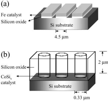
Fig. 1. Schematic diagrams(a) Fe-coated SiO line arrays; (b) SiO2 2 hole arrays with CoSi on the bottom of the hole.x
Table 1
Sample designations and corresponding descriptions
Sample Catalyst Source gases(sccm) Time(min) Temperature(8C) Morphology
1a Fe CHyH s10y100
4 2 6 ;680 Hollow CNTs
2 Fe CH4yH yN s10yy100y1002 2 5 ;700 Bamboo-like CNTs
3 Fe CH4yH s1y1002 30 ;650 Amorphous conical nano-rods
4 Fe CH4yH s1y1002 120 ;650 Amorphous conical nano-rods
5 CoSix CH4yH s1y1002 30 ;650 Amorphous conical nano-rods
6b CoSi
x CH4yH s10y1002 10 ;680 Hollow CNTs
The patterned Si wafer with parallel line arrays. a
The patterned Si wafer with hole arrays. b
and holes, as shown in Fig. 1, by a MPCVD system with source gases of CH qH or CH qH qN . Two4 2 4 2 2 kinds of catalytic films were employed on Si and on the patterned wafers before carbon nanostructures synthesis:
(1) Fe film (20 A) and (2) Co film (75 A) followed˚ ˚
by two-step rapid thermal annealing (RTP) at 600 8C for 60 s and 760 8C for 20 s, under N ambient. The2 solid-state interaction between Si substrate and Co film causes the formation of CoSi phase. Patterned CoSix x arrays with CoSi catalysts at the bottom of the holesx were prepared by photolithography of the Si semi-conductor process, in which the CoSi film is formedx by RTP and the self-aligned silicide process
(SALICI-DE) w16x. CNTs or carbon nano-rods were synthesized
as follows.(1) Reduction in H plasma at 0.67 kPa for2 10 min at a microwave power of 500 W;(2) introduction of CH4yH or CH yN yH process gases at a pressure2 4 2 2 of 2.13 kPa, and a microwave power of 800 W. Table 1 lists the process conditions and the results. The deposi-tion temperatures were estimated by placing a thermo-couple under the substrate holder.
The composition gradient of CoSi film before nano-x structures deposition was examined by Auger electron spectroscopy. Depth profile analysis indicates that the surface compositions are equivalent to CoSi. The mor-phologies and microstructures of the nanostructures were identified by SEM and TEM. FE properties were eval-uated by I–V measurement at 10y6 Torr with an elec-trode-separation of 100 mm.
3. Results and discussion
3.1. Nanostructures morphologies on line arrays and on flat substrate
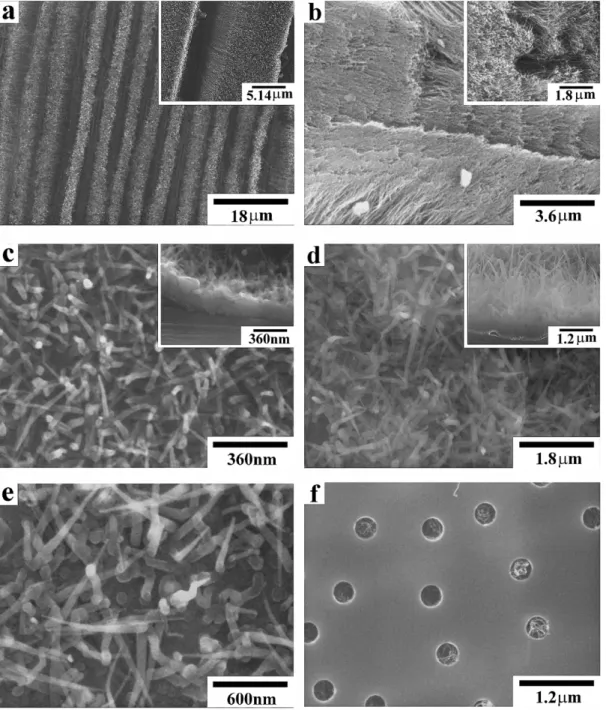
The process conditions in this study can be divided into two series. The first uses different source gases, either CH4yH s10y100 sccm2 (Sample 1) or CH yH y4 2 N s102 y100y100 sccm gases (Sample 2). The second uses the same source gases but different catalysts, either Fe catalysts(Samples 3 and 4) or CoSi catalyst (Sam-x ple 5). For the first series, Fig. 2a presents the mor-phologies of CNTs (Sample 1) on the patterned Si wafers with Fe as catalysts. According to this figure, the CNTs of 18 mm in length are selectively deposited on the Fe-coated line arrays at a deposition rate of 3 mmymin. The CNTs are essentially well-aligned, uni-form in size and perpendicular to the substrate. In contrast to Sample 1, Fig. 2b displays the SEM mor-phology of the well-aligned CNTs of Sample 2 synthe-sized by adding N2 gas into CH4yH2 gases in the reaction chamber, and indicates decrease in deposition
rate(9 mm in length, deposition rate of 1.8 mmymin).
Well-aligned CNTs have been reported elsewhere in Refs. w17–24x. Their growth mechanisms have attracted much interest. The proposed mechanisms include, the preferential etching of CNTs or carbon nano-fibers (CNFs) w17x, van der Waals interactions between neigh-boring CNTs w18x; crowding effect w19x, negative bias application w20x, electrostatic force effect by plasma, that is, plasma-induced alignment w21x, coulomb attrac-tion w22x, external applied field w23x and others. Recent-ly, Merkulov et al. proposed a model that explains the alignment process as a result of a feedback mechanism associated with a nonuniform stress (part tensile, part
Fig. 2. SEM micrographs(a) views of Sample 1 at two magnifications; (b) views of CNTs of Sample 2 at two magnifications; (c)
top-view and cross-section top-view of Sample 3;(d) top-view and cross-section view of Sample 4; (e) top-view of Sample 5; (f) top-view of Sample
6.
compressive) that is created across the interface of catalyst particle w24x. Applying the above mechanisms to the present results is interesting. The electrostatic force induced by the plasma can generate highly oriented and fast carbon ions. This promotes the growth of oriented CNTs. However, fluctuation may occur during the synthetic process, in which situation, the crowding of neighboring CNTs due to initially dense catalyst particles dominates the explanations of the alignment
mechanism, and the growth of freestanding CNTs or CNFs could be difficult in this case.
For the second series, in which the source gases are the same but the catalyst materials differ, Fig. 2c and d depict the morphologies of carbon nano-rods synthesized with different deposition times of 30 min and 2 h but with a fixed gas source ratio (CH yH ) and catalyst4 2 (Fe), respectively. Notably, randomly oriented nano-rods with cone shape are obtained instead of the aligned
222 H.L. Chang et al. / Thin Solid Films 420 – 421 (2002) 219–224
Fig. 3. TEM microstructures(a) hollow CNTs of Sample 1; (b)
bam-boo-like CNTs of Sample 2.
CNTs as shown in Fig. 2a and b. Increasing deposition time lengthens the nano-rods from 0.6 to 3.6 mm without changing their conical shape. Similarly, cone-shaped carbon nano-rods are obtained under the same process conditions except when the Fe catalysts are replaced by CoSi catalysts, as shown in Fig. 2e. In addition, thex CoSi catalysts increase the deposition rate more thanx does the Fe catalysts. In summary, carbon nanostruc-tures, such as CNTs or carbon nano-rods, can be con-trolled by manipulating the compositions and the ratios of the gases, and the catalyst materials.
3.2. Growth of CNTs in the hole arrays
Selective growth of CNTs using CoSi catalysts wasx studied, to develop the CNTs for applications in micro-electronic devices. Fig. 2f shows selective CNTs depo-sition applied on a patterned Si wafer with hole(aspect ratios6) arrays; the CNTs are selectively deposited in the holes. The SEM graph reveals that the selectivity of the process is quite high and the CNTs are wrapped inside the holes with a tube diameter of ;15 nm, rather than being well-aligned CNTs as shown in Fig. 2a, under the same process conditions. The possible reason for the wrapping of the CNTs in the holes is the local circular flow of gases in each hole.
3.3. TEM images and the formation mechanisms of the nanostructures
Fig. 3a and b illustrate the microstructures of the CNTs, obtained by TEM for Samples 1 and 2,
respec-tively. Comparing Fig. 3 a and b reveals that bamboo-like CNTs are formed rather than hollow CNTs by adding N to the source gases. The bamboo-like nano-2 tube is a hollow tube that consists of many interior compartments. Mechanisms of formation have been the subject to many debates w25–29x. The precipitations of graphite sheets are formed as a cap on the surface of the catalytic particle, and then these graphite sheets may slide out of the catalytic particle when the accumulated stress reaches a certain value. The above cycle is repeated to yield a series of compartments that become bamboo-like CNTs. The N gas introduction may change2 the diffusion paths of carbon atoms in the catalyst particles, forming the cap on the catalyst particles. Also, it increases the bending stress of the cap by replacing carbon sites with nitrogen, changing the bonding to pentagonal, heptagonal, or another type. The bending stress of the cap may accumulate beyond the point, at which the cap gradually slides out from the catalyst particle. The formation of the bamboo-like CNTs basi-cally uses the catalyst particle as template for duplicating the caps of the nanotubes.
Fig. 4a and b depict the microstructures of carbon nano-rods, obtained by TEM, using Fe as the catalysts at deposition time of 30 min and 2 h for Sample 3 and Sample 4, respectively. The TEM sample for nano-rods, shown in Fig. 4a, was prepared by ultrasonic dispersion on the grid and in Fig. 4b by mechanical polishing and ion milling. Notably, the nano-rods, shown in both graphs, consist of conical sidewalls and the inner fine channel filled with catalyst material. According to Fig. 4 b, catalysts were embedded in the substrate, signifying a base growth mechanism. The formation of the inside channel in the nano-rod is related to the catalyst, in a manner similar to how the catalyst assists the formation of hollow CNTs. Possible reasons for filling of the inner channel with the catalyst are caused by the capillary force and the suction of the channel under vacuum. A lower carbon concentration(CH yH s0.01) in the plas-4 2 ma atmosphere favors the formation of a gas-tight channel in the nano-rods. As the nano-rod grows out-ward, the nano-rod creates a vacuum in the channel to suck liquid catalyst. The carbon atoms continually deposit on the sides of inner channel along the deposi-tion time, the cone shaped nano-rod is thus formed. This is in agreement with production of some voids, by sucking Fe into channel, observed at the interface between Si substrate and Fe catalyst. Notably, most nano-rods at the deposition time of 2 h (Fig. 4b) are not delaminated after mechanical polishing for TEM sample preparation. A stronger chemical Fe–silicide bond may be formed by prolonged heating or deposition. Another significant feature of Fig. 4a and b is that the deposition conditions are the same as in diamond film or diamond like film synthesis, except when the Fe catalyst is applied w30,31x. This feature may open the
Fig. 4. TEM microstructures of various conical nano-rods(a) top-view of Sample 3; (b) cross-section view of Sample 4.
Fig. 5.(a) J–E curves of hollow CNTs and bamboo-like CNTs (Samples 1 and 2); (b) and (c) the corresponding F–N plots of (a).
way to exploring the deposition mechanisms of dia-mond, CNTs and other nanostructures, all of which made of carbon atoms. The nano-rods could have a structure similar to the diamond-like carbon (DLC) structure. Further study is required.
3.4. Field emission properties
The FE properties of CNTs depend on the geometric enhanced factor (GEF), effective emission sites and
microstructures. The other variables, such as the FE measurement tool, surface contamination, modifications of the surface after testing, and arcing effect are also considered to be crucial w32x. Fig. 5a compares the J– E curves of CNTs prepared with different source gases (Samples 1 and 2). Fig. 5b and c present the correspond-ing Fowler–Nordheim (F–N) plots for Samples 1 and 2, respectively. The turn-on electric fields at a current density of 1 mmycm are 2.71 and 3.87 Vymm for2 Samples 1 and 2, respectively. Also, the current density
224 H.L. Chang et al. / Thin Solid Films 420 – 421 (2002) 219–224
of 1 mAycm , required for a flat panel display w33x, is2 obtained at 3.97 and 5.9 Vymm for Samples 1 and 2, respectively. The higher turn-on electric field and lower current density for Sample 2 than for Sample 1 are considered to be due to the bamboo-like structure and greater tube diameter. The GEF of Sample 2 is therefore reduced.
4. Conclusions
This work develops the synthesis processes to selec-tively deposit different carbon nanostructures, including CNTs and carbon nano-rods, on patterned or un-pat-terned Si substrates using Fe and CoSi as catalysts.x Effects of N addition, catalyst materials and carbon2 concentration on the formation of various nanostructures were studied. The results show that adding nitrogen is crucial to the formation of bamboo-like CNTs. A pos-sible mechanism is also proposed. Various carbon nano-structures, such as the aligned CNTs, the nested CNTs and nano-rods are synthesized by manipulating the carbon and nitrogen concentration in the source gases, the catalyst and the patterned substrate. To the authors’ knowledge, this work successfully deposits CNTs in the small hole arrays with a diameter -0.33 mm for the first time. The work has promising application in the fabrication of microelectronic devices.
Acknowledgments
The authors would like to thank the supports of the National Science Council (Contract No.: NSC90-2216-E-009-034, -035 and -040) and the Ministry of Educa-tion of Taiwan (Contract No.: 89-E-FA06-1-4).
References
w1x S. Iijima, Nature(Lond.) 354 (1991) 56.
w2x M.M.J. Treacy, T.W. Ebbesen, J.M. Gibson, Nature (Lond.)
381(1996) 678.
w3x T.W. Ebbseen, H.J. Lezec, H. Hiura, J.W. Bennett, H.F. Ghaemi,
T. Thio, Nature 382(1996) 54.
w4x W.A. de Heer, W.A. Chatelain, D.A. Ugarte, Science 270 (1995) 1179.
w5x J. Liu, A.G. Rinzler, H. Dai, J.H. Hafner, R.K. Bradley, P.J.
Boul, A. Lu, T. Iverson, K. Shelimov, C.B. Huffman, F.
Rodriguez-Macias, Y.S. Shon, T.R. Lee, D.T. Colbert, R.E. Smalley, Science 280(1998) 1253.
w6x H. Dai, J.H. Hafner, A.G. Rinzler, D.T. Rinzler, D.T. Colbert,
R.E. Smalley, Nature 384(1996) 147.
w7x F. Ito, K. Konuma, A. Okamoto, J. Appl. Phys. 89 (2001)
8141.
w8x G. Che, B.B. Lakshmi, E.R. Fisher, C.R. Martin, Nature 384 (1996) 147.
w9x P.G. Collins, A. Zettle, H. Bando, A. Thess, R.E. Smally,
Science 278(1997) 100.
w10x G. Che, B.B. Lakshmi, E.R. Fisher, C.R. Martin, Nature 393 (1998) 346.
w11x Q. Zhao, J.R. Wood, H.D. Wagner, Appl. Phys. Lett. 78(2001)
1748.
w12x C. Journet, W.K. Maser, P. Bernier, A. Loiseau, M.
Lamy de la Chapelle, S. Lefrant, P. Deniered, R. Lee, J.E. Ficher, Nature 308(1997) 756.
w13x N.R. Franklin, H. Dai, Adv. Mater. 12(2000) 890.
w14x Y.H. Lee, Y.T. Jang, C.H. Choi, D.H. Kim, C.W. Lee, J.E. Lee,
Y.S. Han, S.S. Yoon, J.K. Shin, S.T. Kim, E.K. Kim, B.K. Ju, Adv. Mater. 13(2001) 1371.
w15x Y.S. Han, J.K. Shin, S.T. Kim, J. Appl. Phys. 90(2001) 5731. w16x K.K. Ng, W.T. Lynch, IEEE Trans. Electron. Devices ED-34
(1987) 503.
w17x S.H. Tasi, C.W. Chao, C.L. Lee, H.C. Shih, Appl. Phys. Lett.
74(1999) 3462.
w18x S. Fan, M.G. Chapline, N.R. Franklin, T.W. Tombler, A.M.
Cassell, H. Dai, Science 283(1999) 512.
w19x R. Andrews, D. Jacques, A.M. Rao, F. Derbyshire, D. Qian,
X. Fan, E.C. Dickey, J. Chen, Chem. Phys. Lett. 303(1999)
467.
w20x C.H. Lin, H.L. Chang, C.T. Kuo, Diam. Relat. Mater. 11 (2002) 922.
w21x C. Bower, W. Zhu, S. Jin, O. Zhou, Appl. Phys. Lett. 77 (2000) 830.
w22x Y. Avigal, R. Kalish, Appl. Phys. Lett. 78(2001) 2291. w23x A. Srivastava, A.K. Srivastava, O.K. Srivastava, Carbon 39
(2001) 201.
w24x V.I. Merkulov, A.V. Melechko, M.A. Guillorn, D.H. Lowndes,
M.L. Simpson, Appl. Phys. Lett. 79(2001) 2970. w25x Y. Saito, Carbon 33(1995) 979.
w26x C.J. Lee, J. Park, Appl. Phys. Lett. 77(2000) 3397. w27x V.V. Kovalevski, A.N. Safronov, Carbon 36(1998) 963. w28x X. Ma, E.G. Wang, Appl. Phys. Lett. 78(2001) 978. w29x H.L. Chang, C.H. Lin, C.T. Kuo, Diam. Relat. Mater. 11
(2002) 793.
w30x R. Spitzl, V. Raiko, R. Heiderhoff, H. Gnaser, J. Engemann,
Diam. Relat. Mater. 4(1995) 563.
w31x S.L. Sung, X.J. Guo, K.P. Huang, F.R. Chen, H.C. Shih, Thin
Solid Films 315(1998) 345.
w32x V.I. Merkulov, D.H. Lowndes, L.R. Baylor, S. Kang, Solid
State Electron. 45(2001) 949.
w33x G.A.J. Amaratangta, S.R.P. Silva, Appl. Phys. Lett. 68(1996)