674 IEEE ELECTRON DEVICE LETTERS, VOL. 34, NO. 5, MAY 2013
A Latchup-Immune and Robust SCR Device for
ESD Protection in 0.25-
µm 5-V CMOS Process
Yu-Ching Huang and Ming-Dou Ker, Fellow, IEEE
Abstract— Based on good electrostatic discharge (ESD) robust-ness, silicon-controlled rectifier (SCR) device is used for on-chip ESD protection. The major concern of SCR is the latch-up issue, because of its low holding voltage. Previous papers tried to design latchup-immune SCR devices; however, those devices would cause lower ESD robustness. In this letter, a new latchup-immune and robust SCR device for ESD protection is proposed and verified in a 0.25-µm 5-V CMOS process. Through inserting one additional parasitic bipolar junction transistor into SCR device structure, this new proposed SCR can increase the holding voltage without causing degradation on its ESD robustness.
Index Terms— Electrostatic discharges (ESD), latchup, silicon-controlled rectifier (SCR).
I. INTRODUCTION
S
ILICON-controlled rectifier (SCR) device is known as an efficient device for electrostatic discharge (ESD) protec-tion as it can have the highest ESD robustness in the smallest layout area [1]. However, the main concern of SCR device used in CMOS ICs is the latchup issue. Some noises may mistrigger the SCR device during normal circuit operations to cause the IC function failure.Three conventional methods are presented to solve the latchup problem in previous papers. The first method is to increase the triggered current of SCR [2], [3]. In addition, some additional epitaxial or isolation layers are used to improve latchup immunity of the SCR for ESD protection [4], [5]. The second method is to dynamically modulate the holding voltage of SCR. The idea of dynamic holding voltage is to adjust the holding voltage of SCR by changing the gate bias of the embedded nMOS and pMOS to avoid latchup issue [6]. The third method is to increase the SCR holding voltage [7], [8]. If the holding voltage of SCR is higher than the normal supply voltage, it will be free from latchup issue. This method may decrease the ESD robustness because of the higher heat generation during ESD current discharging. Therefore, it is still a challenge to design an ESD-robust and latchup-immune SCR device within small layout area. In this letter, a new design is proposed to increase the holding voltage
Manuscript received January 30, 2013; revised March 2, 2013; accepted March 8, 2013. Date of publication April 1, 2013; date of current version April 22, 2013. This work was supported in part by the National Science Council, Taiwan, under Contract NSC 101-2220-E-009-020, Contract NSC 101-2221-E- 009-141, and Contract NSC 101-3113-P-110-004. The review of this letter was arranged by Editor W. Ng.
The authors are with the Institute of Electronics, National Chiao Tung University, Hsinchu 30010, Taiwan (e-mail: [email protected]).
Color versions of one or more of the figures in this letter are available online at http://ieeexplore.ieee.org.
Digital Object Identifier 10.1109/LED.2013.2252456
(a) (b)
Fig. 1. (a) Cross-sectional view. (b) Equivalent circuit of conventional SCR.
(a) (b)
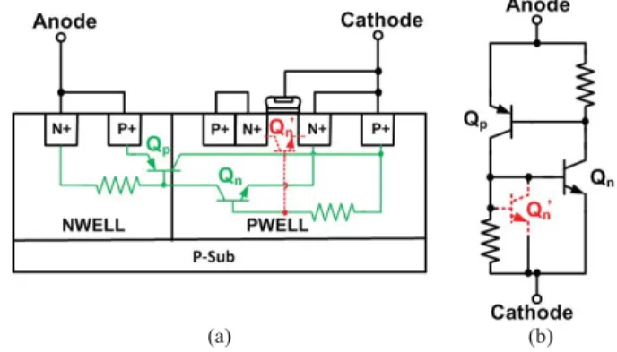
Fig. 2. (a) Cross-sectional view. (b) Equivalent circuit of new proposed SCR with high latchup immunity.
of the SCR device without decreasing its ESD robustness in a compact layout area.
II. DEVICESTRUCTURES
Two SCR structures are compared in this letter, which are labeled as the conventional SCR and the new proposed SCR, respectively. The cross-sectional view of the conventional SCR is shown in Fig. 1(a). The equivalent circuit of the conventional SCR is shown in Fig. 1(b) with the parasitic BJTs and resistors. During ESD stress, the NPN BJT (Qn) may turn on first, and then it will help the PNP BJT (Qp) to be turned on. The positive feedback of those two BJTs in SCR [9] is the reason why SCR can have such low holding voltage.
To improve latchup immunity, the new structure of SCR is shown in Fig. 2. To increase the holding voltage of SCR, one more parasitic BJT (Qn’) is inserted into the device structure, which is shown in Fig. 2(a). The equivalent circuit of the new proposed SCR is shown in Fig. 2(b). During the turn-on
HUANG AND KER: LATCHUP-IMMUNE AND ROBUST SCR DEVICE 675
(a)
(b)
Fig. 3. TLP measurement results. (a) Conventional SCR. (b) New proposed SCR.
operation of the SCR, the NPN BJT (Qn) and the additional parasitic BJT (Qn’) turn on at the same time. The additional BJT (Qn’) clamps the voltage between base and emitter of the NPN (Qn), which makes the positive feedback of BJTs weaken. That is, the additional BJT (Qn’) will break the pos-itive feedback of the NPN and PNP BJTs. Hence, the holding voltage of this new proposed SCR will be higher than that of the conventional SCR. Therefore, the new proposed SCR can be free from latchup problem. A dummy gate is added to reduce the base width of the additional BJT (Qn’), which is the spacing between the two N+ diffusions of collector and emitter. The dummy gate is connected to the cathode of SCR to turn off the channel beneath of dummy gate. The current gain of the additional BJT (Qn’) can be further increased by using a shorter channel length of dummy gate in the inserted NMOS. The new proposed SCR is fully process-compatible to the commercial CMOS processes without additional mask or process step in the chip fabrication.
This design is fabricated in a 0.25-µm 5-V process. The total widths of all test SCR devices are drawn as 200µm for performance comparison. All of the test devices occupy the same layout area.
III. EXPERIMENTALRESULTS
A. TLP Test
A transmission-line-pulsing (TLP) system is used to measure the breakdown voltage, holding voltage, and the
Fig. 4. Measurement setup of TLU test [10].
maximum current-handling ability (the second breakdown current, It2) of the fabricated devices. The failure criterion is
defined as the leakage current over 1µA under the 5-V bias condition.
The TLP measurement results of the fabricated SCR devices are shown in Fig. 3. In Fig. 3(a), the breakdown voltage of the conventional SCR structure is ~22 V and the holding voltage is ~3 V. Therefore, it may suffer the latchup issue by noise triggering in the normal operation condition with VDD of 5 V.
Comparing with the measurement result of the new proposed SCR in Fig. 3(b), the holding voltage of the new proposed SCR is increased to ~7.7 V, whereas the breakdown voltage unchanged. The maximum current-handling ability (It2) of the
new proposed SCR is not degraded, which is still as high as ~7.5 A. Additional ESD-detection circuit [1] can be used to trigger the proposed SCR on, during ESD events.
B. ESD Robustness
To make sure that the ESD robustness of the new pro-posed SCR is not degraded, the human-body-mode (HBM) and machine-mode (MM) ESD tests are performed to the fabricated devices by the ESD tester. The failure criterion is defined with 30% of breakdown voltage shift after ESD stress. The conventional SCR can pass 8-kV HBM and 800-V MM ESD tests, which are the voltage limitation of a given ESD tester. The new proposed SCR can also pass the 8-kV HBM and 800-V MM ESD tests. This result confirms that the new proposed SCR does not degrade the ESD robustness.
C. TLU Test
Transient overshoots on power-supply voltage can take place because of the noise coupling under system or environment disturbance. Those overshoots may let SCR be mistriggered. The transient-induced-latchup (TLU) test is to simulate the noise condition under the normal operation. The TLU setup is shown in Fig. 4 [10], where the MM ESD source is used to generate the transient noise into the power supply of device under test. Therefore, the parasitic BJTs in SCR may be mistriggered by such transient noise. If it is affected by the latchup issue, the voltage waveform monitored in the oscilloscope will be clamped down to its holding voltage after transient noise triggering.
676 IEEE ELECTRON DEVICE LETTERS, VOL. 34, NO. 5, MAY 2013
(a)
(b)
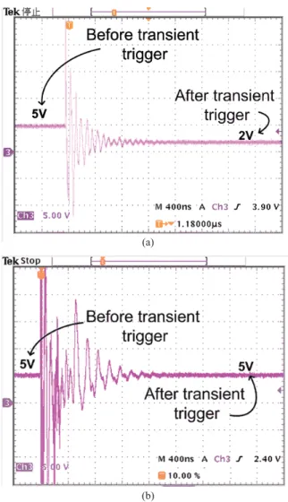
Fig. 5. Voltage waveforms before/after transient noise triggering. (a) Conventional SCR. (b) New proposed SCR, during TLU test.
The test results of the fabricated SCR devices are shown in Fig. 5. In Fig. 5(a), after transient noise triggering with the initial Vcharge of only 50 V, the voltage is clamped down to
~2 V. On the contrary, the voltage across the new proposed SCR is still kept at 5 V, as shown in Fig. 5(b), even if the
Vcharge is up to 800 V during the TLU test. This result has
proved that the new proposed SCR is a high latchup-immune device for 5-V circuit applications.
IV. CONCLUSION
A new SCR device was proposed and verified in a 0.25-µm 5-V CMOS process, which performed both of high ESD robustness and high latchup immunity in the same layout area, as compared with the convention SCR device. The new proposed SCR was fully process-compatible to the general CMOS processes without additional mask or process step in the chip fabrication. This new proposed SCR will be a good solution of ESD protection for 5-V circuit applications in the commercial IC products.
REFERENCES
[1] M.-D. Ker and K.-C. Hsu, “Overview of on-chip electrostatic discharge protection design with SCR-based devices in CMOS integrated cir-cuits,” IEEE Trans. Device Mater. Rel., vol. 5, no. 2, pp. 235–249, Jun. 2005.
[2] M. Mergensa, C. Russb, K. Verhaegea, J. Armerb, P. Jozwiakb, and R. Mohnb, “High holding current SCRs (HHI-SCR) for ESD protection and latch-up immune IC operation,” Microelectron. Rel., vol. 43, no. 7, pp. 993–1000, Jul. 2003.
[3] M.-D. Ker, “Lateral SCR devices with low-voltage high-current trig-gering characteristics for output ESD protection in submicron CMOS technology,” IEEE Trans. Electron Devices, vol. 45, no. 4, pp. 849–860, Apr. 1998.
[4] G. Meneghesso, A. Tazzoli, F. Marino, M. Cordoni, and P. Colombo, “Development of a new high holding voltage SCR-based ESD pro-tection structure,” in Proc. IEEE Int. Rel. Phys. Symp., Apr. 2008, pp. 3–8.
[5] Z. Liu, J. Liu, and J. Vinson, “Novel silicon-controlled rectifier (SCR) for high-voltage electrostatic discharge (ESD) applications,” IEEE
Elec-tron Device Lett., vol. 29, no. 7, pp. 753–755, Jul. 2008.
[6] M.-D. Ker and Z.-P. Chen, “SCR device with dynamic holding volt-age for on-chip ESD protection in a 0.25-µm fully salicided CMOS process,” IEEE Trans. Electron Devices, vol. 51, no. 10, pp. 1731–1733, Oct. 2004.
[7] S. Bart, B. Ilse, M. Olivier, and K. Bart, “On-chip ESD protection with improved high holding current SCR (HHISCR) achieving IEC 8 kV contact system level,” in Proc. 32nd Electr. Overstress Electrostat.
Discharge Symp., Oct. 2010, pp. 167–175.
[8] S. Dong, J. Wu, M. Miao, J. Zeng, Y. Han, and J. J. Liou, “High-holding-voltage silicon-controlled rectifier for ESD applications,”
IEEE Trans. Electron Device Lett., vol. 33, no. 10, pp. 1342–1347,
Oct. 2012.
[9] M.-D. Ker and C.-Y. Wu, “Modeling the positive-feedback regenerative process of CMOS latchup by a positive transient pole method. I. The-oretical derivation,” IEEE Trans. Electron Devices, vol. 42, no. 6, pp. 1141–1148, Jun. 1995.
[10] M.-D. Ker and S.-F. Hsu, “Component-level measurement for transient-induced latchup in CMOS ICs under system-level ESD considera-tions,” IEEE Trans. Device Mater. Rel., vol. 6, no. 3, pp. 461–472, Sep. 2006.
![Fig. 4. Measurement setup of TLU test [10].](https://thumb-ap.123doks.com/thumbv2/9libinfo/7662005.140524/2.918.113.409.78.583/fig-measurement-setup-of-tlu-test.webp)