Growth of SiC Films on Si(lO0) by Electron
Cyclotron Resonance Chemical Vapor Deposition
Using SiH4/CH4/H2
Chih-Chien Liu and Chiapyng Lee
Department of Chemical Engineering, National Taiwan Institute of Technology, Taipei, Taiwan
Kuan-Lun Cheng and Huang-Chung Cheng
Department of Electronics Engineering, National Chiao-Tung University, Hsinchu, Taiwan
Tri-Rung Yew
Materials Science Center, National Tsing-Hua University, Hsinchu, Taiwan
A B S T R A C T
S i C films w e r e deposited o n St(100) substrates b y electron cyclotron resonance chemical v a p o r deposition at 500~ using S i H J C H 4 / H 2 gas mixtures. T h e chemical composition a n d crystalline microstructure w e r e investigated b y x-ray photoelectron spectroscopy a n d cross-sectional transmission electron microscopy, respectively. T h e film composition a n d microstructure are correlated to process variables. T h e deposition m e c h a n i s m w h i c h controls the film characteristics is presented.
Introduction
Silicon carbide (SIC) is an important material for poten- tial applications in photoeleetronics, high temperature semieondueting devices, w e a r resistant coatings, a n d pro- tective barriers for corrosion or thermal oxidation. All these applications are d u e to its u n i q u e properties such as w i d e b a n d g a p , high electron mobility, high thermal con- ductivity, a n d high melting point. Further, S i C can be used as a thin buffer layer for the g r o w t h of d i a m o n d films on silicon substrates. I
Preparation of this material, especially for h a r d coating, is usually p e r f o r m e d b y chemical v a p o r deposition ( C V D ) because of its a d v a n t a g e for f o r m i n g m u l t i e o m p o n e n t , high density, a n d well-crystallized films on the surface of the desired shape. H o w e v e r , S i C films p r o d u c e d b y the C V D m e t h o d are often not stoichiometric but contain excess sil- icon or carbon, causing changes in film properties. There- fore, to obtain a suitable chemical composition a n d crys- talline p h a s e for a specific purpose, it is important to u n d e r s t a n d the m e c h a n i s m w h i c h d e t e r m i n e s the optimal process p a r a m e t e r s for the deposition of the desired film. H o w e v e r , for the deposition of crystalline B-SiC, a high reaction temperature, usually higher than 1000~ 2 is nec- essary a n d limits the application of C V D .
Recently, a f e w researchers h a v e tried to decrease the deposition temperature of crystalline ~-SiC films b y using electron cyclotron resonance chemical v a p o r deposition ( E C R - C V D ) . Diani et al. 3 synthesized monocrystalline ~- S i C (3C-SiC) b y E C R - C V D at temperatures a b o v e 800~ K a t s u n o et al. ~ reported the g r o w t h of microcrystalline S i C thin films at 300~ without identifying the crystalline phase. In previous w o r k ~ the deposition of stoiehiometrie mieroerystalline ~ - S i C at 50O~ b y E C R - C V D f r o m m i x - tures of Sill4, CH4, a n d H2 has b e e n successfully achieved. H o w e v e r , detailed characterization the composition a n d microstrueture of the S i C film deposited b y E C R - C V D a n d film-formation m e c h a n i s m h a v e not b e e n published. T h e p u r p o s e of this w o r k is to correlate the variation of film chemical composition a n d crystalline mierostructure to the deposition parameters. T h e m e c h a n i s m w h i c h governs the correlation is proposed.
Experimental
Substrates used w e r e (i00) oriented, p-type silicon wafers with a resistivity of 5-15 Ft-cm, a n d w e r e cut into 12 • 30 m m size. T h e substrates w e r e cleaned e x s i t u b y a
modified spin-etching m e t h o d 8 to provide a hydrogen-ter- m i n a t e d silicon surface a n d prevent surface oxidation dur- ing air exposure. 7
S i C films w e r e deposited in a c o m m e r c i a l P l a s m a - Q u e s t M o d e l 357 electron cyclotron resonance reactor using C H J SiH4/H2 gas mixtures. Details of the E C R - C V D reactor w e r e described in a previous publication. ~ T h e total pres- sure w a s kept constant at 20 mTorr. T h e C H J S i H 4 flow ratio w a s varied b y c h a n g i n g C H 4 flow rate while keeping Sill4 flow rate at 5 sccm. T h e effect of m i c r o w a v e p o w e r w a s investigated b y keeping the C H 4 a n d Sill4 flow rates at 5 a n d 2.5 sccm, respectively. T h e flow rate of H2 w a s kept constant at I00 scem. T h e deposition time w a s 30 m i n in all cases.
X P S analyses w e r e p e r f o r m e d in a V G Microtech M T - 5 0 0 spectrometer. T h e spectrometer w a s e q u i p p e d with a h e m i - spherical analyzer a n d all x-ray photoelectron spec- troscopy ( X P S ) data presented here w e r e acquired using the M g K ~ x-rays (1253.6 eV). P e a k positions w e r e cali- brated with respect to the C is p e a k at 284.6 e V f r o m the adventitious h y d r o c a r b o n contamination.
T h e crystalline structure of the deposited film w a s e x a m - ined in a J E O L 2 O 0 C X S T E M . T h e samples used for cross- sectional transmission electron m i c r o s c o p y ( X T E M ) in- spection w e r e cut into 3 • 6 m m size. T h e X T E M is a destructive analysis technique to observe the deposited film with electron b e a m s perpendicular to the w a f e r sur- face normal. A s X T E M can be used to observe the deposited film a n d the film/substrate interface simultaneously, it b e c o m e s the m o s t direct a n d precise w a y to determine the crystalline p h a s e a n d lattice constant of the depos- ited films.
Results
T h e i n d e p e n d e n t process variables in our deposition pro- cess that determine the film composition a n d micro- structure are the following, (i) m e t h a n e to silane flow ratio ( C H J S i H 4 ) as m e a s u r e d in relative flow rates, a n d (it)
the m i c r o w a v e power. In this section w e present the in- fluences of these parameters on film composition a n d mierostructure.
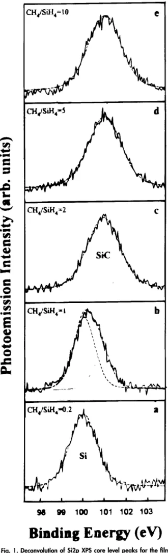
E x p e r i m e n t s with varied C H J S i H 4 flow ratios w e r e car- ried out at a fixed Sill4 flow rate of 5 s c e m with the C H 4 flow rate varying f r o m i to 50 secm. T h e m i c r o w a v e p o w e r w a s kept constant at 1200 W. Figure 1 s h o w s high resolu- tion X P S spectra of Si 2p p e a k s for various C H 4 / S i H 4 flow ratios. T h e binding energies for Si a n d S i C are i00 a n d
4280
J. Electrochem. Soc.,
Vol. 142, No. 12, December 1995 9 The ElectrochemicalSociety,
Inc. C H d S i H 4 = | 0 ,,i 9CH+/SiH4=2
C
e ~cHd
b
a
i I I * * I98
~
100
101 102 103
Binding Energy (eV)
Fig. 1. Deconvalution of Si2p XPS core level peaks for the films
deposited at various C H J S i H 4 flow ratios.
O ~ e~ @ r ~ 1 0 0 9
(
60 40 0 9 ! J | 0 2 r 1 4 1 ~ I t I 6 g l0 C H 4 / S i H 4 F l o w R a t i oFig. 2. SiC composition in the films deposited at various CH4/SiH4 flow ratios.
101.3 eV, respectively. T h e binding energies m e a s u r e d here are slightly deviated f r o m those obtained b y other re- searchers, 8 but a n energy difference A - S i C (C is-Si 2p) of 182.2 e V is in a g r e e m e n t with those reported. 8'9 Figure la s h o w s that only Si is f o r m e d at a C H J S i H 4 flow ratio of 0.2. W h e n the C H ~ / S i H 4 flow ratio is increased to 1 (Fig. lb), the Si 2p p e a k shifts to a binding energy b e t w e e n elemental Si a n d S i C because of overlap of peaks. T h e Si 2p X P S s p e c t r u m s h o w n in Fig. ib could be deconvoluted into Si (i00 eV) a n d S i C (101.3 eV) b y a s s u m i n g Gaussian- Lorentzian type distributions. T h e composite curves of the t w o c o m p o n e n t s m a t c h the experimental spectra well. F r o m Fig. I, it can be f o u n d that as the C H J S i H 4 flow ratio is increased to 2 a n d higher, only S i C is formed. T h e film compositions w e r e estimated f r o m the p e a k area of each c o m p o n e n t after normalizing with the respective relative sensitivity factor. I~ A c c o r d i n g to Fig. I, changes in the S i C composition of the film as a function of the C H 4 / S i H 4 flow ratio can be obtained, as s h o w n in Fig. 2.
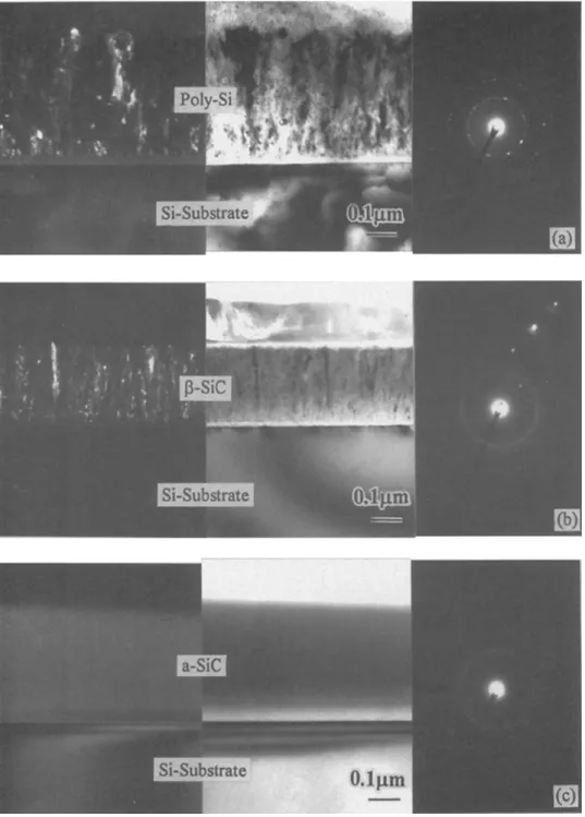
Figure 3 s h o w s cross-sectional T E M ( X T E M ) dark-field a n d bright-field m i c r o g r a p h s with electron diffraction pat- terns of the films g r o w n at different C H 4 / S i H 4 flow ratios. Figure 3a indicates that at a C H J S i H 4 flow ratio of I (same as in the case of the flow ratio of 0.2), the deposited films on Si are of polyerystalline Si (poly-Si) d e t e r m i n e d b y the ring spacing of lhe eleclron diffraction pattern. T h e grains s h o w n in the dark-field i m a g e (Fig. 3a) w e r e of Si, since they are taken f r o m the Si<lll> ring in diffraction pattern. T h e Si 2p p e a k (Fig. Ib) s h o w s the existence of SiC w h i c h could hardly be observed in the diffraction pattern of Fig. 3a. This m a y be because S i C is of an a m o r p h o u s f o r m a n d the a m o u n t of S i C is too small to be m o n i t o r e d b y X T E M . W h e n the C H J S i H 4 flow ratio w a s increased to 2, the microcrystalline [~-SiC could be deposited as s h o w n in Fig. 3b. U s i n g the spot diffraction pattern of < I i 0 > Si zone in Fig. 3b as a reference, the film is identified to be zinc- blende structure with a lattice constant of 0.434 -+ 0.006 n m , w h i c h is identical to that of bulk g-SiC. ~ T h e grains s h o w n in the dark-field i m a g e are of S i C since they w e r e taken f r o m the S i C < l l i> ring in the diffraction pattern. A t C H 4 / S i H 4 flow ratios a b o v e 2, a m o r p h o u s S i C (a-SiC) w a s observed. T h e typical X T E M m i c r o g r a p h of a m o r p h o u s S i C is s h o w n in Fig. 3c w h i c h w a s deposited at a C H J S i H 4 flow r a t i o of 10. T h e r e f o r e , a C H J S i H 4 f l o w r a t i o of 2 is c r u c i a l f o r c r y s t a l l i n e g - S i C f o r m a t i o n a c c o r d i n g to o u r a f o r e m e n - t i o n e d r e s u l t s a t v a r i o u s f l o w r a t i o s . I t is n o t c l e a r w h y a t h i n a m o r p h o u s l a y e r e x i s t s b e t w e e n t h e d e p o s i t e d f i l m a n d s u b s t r a t e i n Fig. 3a a n d b. E x p e r i m e n t s w i t h v a r i e d m i c r o w a v e p o w e r s w e r e c o n - d u c t e d a t a f i x e d Sill4 f l o w r a t e of 5 sccm. T h e C H J S i H 4 f l o w r a t i o w a s k e p t c o n s t a n t a t 2. F i g u r e 4 s h o w s t h e h i g h - r e s o l u t i o n X P S s p e c t r a of Si 2p p e a k s f o r d i f f e r e n t m i - c r o w a v e p o w e r s . T h e s h i f t p h e n o m e n o n of Si 2p p e a k s is s i m i l a r t o t h a t o b s e r v e d i n Fig. 1 f o r d i f f e r e n t f l o w r a t i o s .
Fig. 3. Dark-field and bright-
field XTEM micrographs and dif-
fraction patterns of the films de-
posited at 500~
a microwave
power of 1200 W, and a CHJ
Sill4 flow ratio of (a) I, (b) 2, and
(c) 10.
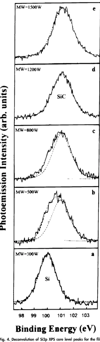
W h e n the m i c r o w a v e p o w e r is increased f r o m 300 to 1500 W, the Si 2p p e a k shifts f r o m the elemental Si to the SiC. This indicates that the a m o u n t of S i C in the deposited thin film increases with the m i c r o w a v e power. Figure 4a s h o w s that only Si is f o r m e d at 300 W. T h e Si 2p X P S spectra for 500 a n d 800 W (Fig. 4b a n d e) also could be deconvoluted into Si a n d SiC. H o w e v e r , w h e n the mi- c r o w a v e p o w e r is increased to 1200 W a n d higher (Fig. 4d a n d e), only S i C is deposited. Figure 5 s h o w s the effect of m i c r o w a v e p o w e r on the composition of S i C in the films.
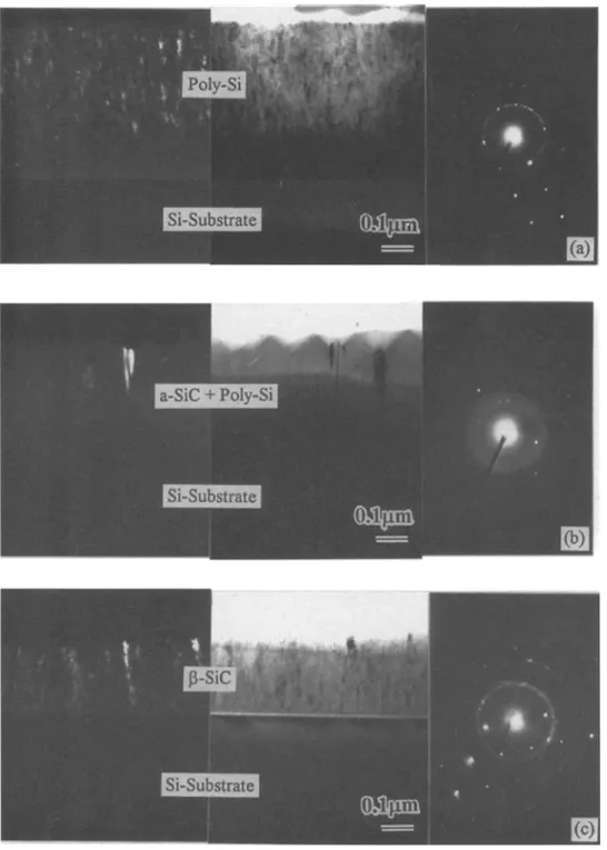
Microstructures of the films g r o w n at different mi- c r o w a v e p o w e r s w e r e investigated a n d the results are s h o w n in Fig. 6. W h e n the m i c r o w a v e p o w e r is 300 W, Fig. 6a indicates that only polycrystalline Si is deposited. At a m i c r o w a v e p o w e r of 500 W, the film w h i c h is c o m p o s e d of a m o r p h o u s S i C a n d e m b e d d e d polycrystalline Si grains (a-SiC + poly-Si) is deposited. This result is s h o w n in Fig. 6b. H o w e v e r , w h e n the m i c r o w a v e p o w e r is increased to 1200 W a n d higher, microerystalline B-SiC films are de- posited as s h o w n in Fig. 6c. Therefore, a sufficient mi- c r o w a v e p o w e r is required to deposit microcrystalline ~- SiC. It is also unclear w h y an a m o r p h o u s layer exists at the interface in Fig. 6a-e.
Discussion
In the present w o r k w e have studied the effects of C H 4 / Sill4 flow ratio a n d m i c r o w a v e p o w e r o n the g r o w t h of microcrystalline B - S i C at 500~ b y E C R - C V D using X P S a n d X T E M .
W e clearly observe in Fig. 3 that w h e n the C H J S i H 4 flow ratio is varied f r o m 0.2 to i0, the crystalline p h a s e is c h a n g e d f r o m the polycrystalline silicon to the microcrys- talline B-SiC, a n d finally to the a m o r p h o u s silicon carbide. In Fig. 6, w h e n the m i c r o w a v e p o w e r increases f r o m 300 to 1500 W, the film microstructure is c h a n g e d f r o m the poly- crystalline Si to the polycrystalline silicon grains e m b e d - d e d in a m o r p h o u s SiC, a n d finally to the mierocrystalline B-SiC. Therefore, to obtain a suitable chemical c o m p o s i - tion a n d microstructure for a specific purpose, it is impor- tant to u n d e r s t a n d the m e c h a n i s m that governs the film formation.
U n d e r the condition of excess h y d r o g e n as in this study, the p l a s m a chemistry of S i H J H 2 has b e e n studied b y Shieh
et al., n,12 a n d that of C H J H ~ b y H s u 13 a n d M i t o m o et al. 14
Shieh et al. 11'12 suggested that Sill4 d e c o m p o s e s in the p l a s m a to p r o d u c e H2 a n d m o r e reactive precursor species
4282
J. Electrochem. Soc.,
Vol. 142, No. 12, December 1995 9 The Electrochemical Society, Inc..=
M W = 5 0 0 Wb
i ! M W = g O O W,'
C
il I & ,i * J 9 8 9 9 100 101 1 0 2 1 0 3Binding Energy (eV)
Fig. 4. Deconvolution of Si2p XPS core level peaks for the films deposited at various microwave powers.
Ioo
o ~ ,~ 60 0 N 4o 0 ~ ~o r~ o 200 1 1 5 i I , i i I , l , 400 600 800 !000 " I I I I 1200 1400 1600 Microwave power (W)Fig. 5. SiC composition in the films deposited at various microwave powers.
S i H x (x = 0, 2, 3), a n d the m a j o r radicals for the deposition of silicon should be S i H ~ (x = 0, 2, 3). Besides, H s u ~3 studied the m i c r o w a v e p l a s m a chemistry of C H J H 2 b y molecular b e a m m a s s spectroscopy ( M B M S ) a n d f o u n d that C H 4 can react w i t h the h y d r o g e n a t o m to f o r m C H 3 w h i c h c a n be converted subsequently into CfH2 in excess H - a t o m . Mit- o m o et al.1~ u s e d Fourier transform infrared (FTIR) spec- troscopy to study the effect of various c a r b o n feed gases. Their reports also c o n f i r m the result of H s u ~3 o n the f o r m a - tion of CfHf. F o r l o w pressure C V D a m o r p h o u s S i C growth, a m e c h a n i s m has b e e n p r o p o s e d b y H o n g et al. ~5,~6 a n d is described as follows. SifH6 d e c o m p o s e s in the gas p h a s e to f o r m SiH~ w h i c h reacts w i t h CfH2 in t w o paths, (i) a reac- tion of the gaseous Sill2 w i t h C ~ H 2 a d s o r b e d o n the surface a n d (it) a gas-phase reaction b e t w e e n gaseous SiHz a n d gaseous C f H 2 to f o r m another intermediate product, m o s t plausibly, S i H 3 ~ C H .
B a s e d o n the a b o v e discussion, the m o s t p r o b a b l e film formation m e c h a n i s m for the present w o r k is p r o p o s e d as follows
i. U n d e r the p l a s m a environment, silane d e c o m p o s e s in the gas p h a s e to f o r m S i H ~ (x = 0, 2, 3) a n d H 2
SiH4(g) --~ SiHx(g) + ~ H2(g) [1] 2. M e t h a n e c a n react w i t h the h y d r o g e n a t o m to f o r m m e t h y l a n d a rapid conversion f r o m m e t h y l to acetylene can be sustained in excess H a t o m
H(g) + CH~(g) ---> H2~) + CH3(g) [2] 2CH3(g) ---> C2H2cg~ + 2H2(~) [3] 3. SiHx m a y r e a c t w i t h CH3 in t w o p a t h s (i) a r e a c t i o n of t h e gaseous SiHx w i t h CH3 a d s o r b e d on t h e surface a n d
(ii)
a g a s - p h a s e r e a c t i o n b e t w e e n gaseous SiHx a n d gaseous CH3 to f o r m an i n t e r m e d i a t e p r o d u c t
3 + x _
SiHx(g) + CH3(~d~ --> SiC(~) + ~ 2i2(~) [4] SiHx(gl + CH3r -+ Intermediate --> SiC(sl [5] 4. SiH~ m a y also react w i t h CfH2 in t w o paths (i) a reac- tion of the gaseous Sill2 w i t h CfH2 a d s o r b e d o n the surface a n d (it) a gas-phase reaction b e t w e e n gaseous Sill 2 a n d gaseous C f H 2 to f o r m a n intermediate product, m o s t plausi- bly S i H 3 ~ C H as p r o p o s e d b y H o n g et al. i~
2SiHf( a + CfH~(ad ) --> 2SiC(~) + 3Hf(gj [6] SiHf(g) + CfHf~g) ---) Si3HC~CH(~) ---> SiC(s) [7] But the real mechanism still needs to be proved by mass spectroscopy analysis which is an interesting subject for future work.
Fig. 6. Dark-field and bright- field XTEM micrographs and dif- fraction patterns of the films de-
p
osited at 500~ a CHJSiH4ow ratio of 2, and a microwave power of (a) 300, (b) 500, and (c) 1500 W.
W i t h the m e c h a n i s m p r o p o s e d above, the formation of various type films at different C H J S i H ~ flow ratios a n d m i c r o w a v e p o w e r s can be explained as follows. Since the b o n d energies of S i - - H a n d C - - H are a b o u t 320 a n d 410 kJ/ tool, 17 respeelively, this suggests that m o s t likely the SiH~ has a higher dissociation efficiency than CH4. A t C H J S i H ~ flow ratios b e l o w 2, since the concentration of C H 4 is too low, the decomposition reaction of Sill4 (Eq. i) should d o m - inate a n d result in m a n y SiHx radicals. T h e SiH~ radicals adsorb onto the Si surface w h e r e they d e c o m p o s e a n d poly- crystalline silicon is deposited (Fig. 3a). A t a C H J S i H 4 flow ratio of 2, relatively larger a m o u n t s of the C H 4 are a d d e d into the system. T h e a m o u n t s of C H 3 radicals a n d C~H2 are c o m p a r a b l e with that of SiHx, so that steps 3 a n d 4 of the m e c h a n i s m could occur to f o r m S i C with a suitable g r o w t h rate (0.159 nm/s) a n d the stoichiometric microcrystalline ~ - S i C film is obtained (Fig. 3b). H o w e v e r , at C H J S i H 4 flow ratios a b o v e 2, it is possible that the g r o w t h rate is too high (0.389 n m / s at C H J S i H ~ = i0) so that the S i C deposited on the Si substrate surface does not h a v e sufficient time to
arrange in an orderly fashion. Therefore, a m o r p h o u s S i C is obtained (Fig. 3c). T h e X P S data (Fig. 1 a n d 2) also s h o w the c h a n g e of film type f r o m poly-Si to S i C a n d the varia- tion of film composition.
W h e n the m i c r o w a v e p o w e r is as l o w as 300 W, the de- posited film is still poly-Si (Fig. 6a) even at a C H J S i H 4 flow ratio of 2. T h a t is still because the energy n e e d e d for SiHx formation is lower than that of C H 4 decomposition a n d the energy is e n o u g h for the subsequent decomposition of SiH~ to occur. H o w e v e r , at 500 W m i c r o w a v e power, the energy supplied b y p l a s m a m a y be e n o u g h for the dissociation of C H 4 so that m o s t SiHx radicals can react with C H 3 radicals a n d C2H2 to f o r m SiC, but m a y not be e n o u g h for surface rearrangement. H o w e v e r , 500 W m a y b e is still too l o w to p r o d u c e a sufficient a m o u n t of C H 3 radicals a n d C2H2. T h e residual SiHx adsorbs onto the Si surface a n d results in the g r o w t h of poly-Si grains. Therefore, a m o r p h o u s S i C a n d e m b e d d e d poly-Si grains can be observed in the film (Fig. 6b). A s the m i c r o w a v e p o w e r is increased to 1200 W a n d higher, the supplied energy is sufficient for both the
4284
J. Electrochem. Soc.,
Vol. 142, No. 12, December 1995 9 The Electrochemical Society, Inc. formation of radicals and the crystallization of amorphousSiC into microcrystalline B-SiC (Fig. 6c). The XPS d a t a (Fig. 4 and 5) also show the change of film t y p e from p o l y - Si to SiC and the variation of film composition.
Conclusion
XPS a n d XTEM were used to study films deposited by ECR-CVD using S i H J C H J H 2 mixtures. When the C H j Sill4 flow ratio were v a r i e d from 0.2 to 10, the crystalline phase of films varie from polycrystalline silicon to the mi- crocrystalline 15-SIC, and finally to amorphous silicon car- bide. As the microwave power increases from 300 to 1500 W, the film microstructure c h a n g e f r o m polycrys- talline Si to polycrystalline silicon grains e m b e d d e d in a m o r p h o u s SiC, a n d finally to microcrystalline [~-SiC. A film-formation m e c h a n i s m is p r o p o s e d to explain the cor- relation b e t w e e n film characteristics (composition a n d mi- crostructure) a n d process variables.
Acknowledgment
This w o r k w a s supported b y Republic of C h i n a National Science Council u n d e r Contract No. N S C 8 4 - 2 1 1 2 - M - 007-036, " T h e study of SiC Blue Light Emitting D i o d e Materials."
M a n u s c r i p t submitted M a r c h 21, 1995; revised m a n u - script received July 27, 1995.
National Taiwan Institute of Technology assisted in
meeting the publication costs of this article.
R E F E R E N C E S
i. E. G. W a n g ,
Physica B,
185, 85 (1993).2. R. F. Davis, G. Kelner, M . Shur, J. W. Palmour, a n d J. A. E d m o n d ,
Proc. IEEE,
79, 677 (1991).3. M . Diani, J. L. Bischoff, L. Kubler, a n d D. Bolmont,
Appl. Surf. Sci.,
68, 575 (1993).4. M. Katsuno, T. Futagi, Y. Ohta, H. Mimura, and K. Ki- tamura,
ibid.,
70/71, 675 (1993).5. C. C. Liu, C. Lee, K. L. Cheng, H. C. Cheng, a n d T. R. Yew,
Appl. Phys. Lett.,
66, 168 (1995).6. C. H. Chen, C. M. W a n , a n d T. R. Yew,
ibid.,
62, 3126 (1993).7. P.J. Grunthaner, F. J. Grunthaner, R. W. Fathauer, T. L. Lin, M. H. Hecht, L. D. Bell, a n d W. J. Kaiser,
Thin
Solid Films,
183, 197 (1989).8. I. Kusunoki and Y. Igari,
Appl. Surf. Sci.,
59, 95 (1992). 9. P. A. Taylor, M. Bozack, W. J. Choyke, and J. T. Yates,J. Appl. Phys.,
65, 1099 (1989).10. D. Briggs and M. P. Seah,
Practical Surface Analysis by
Auger and X-Ray Photoelectron Spectroscopy,
John Wiley & Sons, New York (1983).11. ~I. D. Shieh, C. Lee, and T. R. Yew,
This Journal,
141, 3584 (1994).12. M. D. Shieh, C. Lee, C. H. Cheng, T. R. Yew, and C. Y. Kung,
Appl. Phys. Lett.,
63, 1252 (1993).13. W. L. Hsu,
J. Appl. Phys.;
72, 3105 (1992).14. T. Mitomo, T. Ohta, E. Kondoh, and K. Ohtsuka,
ibid.,
70, 4532 (1991).15. L. S. Hong, Y. Shimogaki, Y. Egashira, and H. Komiyamd,
This Journal,
139, 3653 (1992).16. I. S. Hong, Y. Shimogaki, a n d H . Komiyama,
J. Phys. C,
I, 2 (1991).17. I. S. Butler a n d J. F. Harrod,