Sub-mW 5-GHz Receiver Front-End Circuit
Design
Tatao Hsu, Yen-Lin Liu, Shu-Hui Yen, and
Chien-Nan Kuo
National Chiao Tung
University,
Hsinchu,
Taiwan
Abstract - In this work a 5-GHz receiver front-end is
designedfor theapplicationof wireless sensor networks. The circuit topology is chosen available for low supply voltage
below 1V. The stability condition of the LNA circuit is ensured by adding reactive components. Total power
consumption of the fabricated circuit is 0.86mW, of which 0.7mW goes to the LNA stage. The measured return loss and conversion gain are 11dB and 25dB, respectively. The noise
figureis 12dB and the IIP3 is around -6.5dBm.
Index Terms - Low power design, low-noise amplifier,
single-balancedmixer.
I.INTRODUCTION
Ultra-lowpowerconsumption is criticaltotheemerging application of wireless sensor networks. It allows long
lasting use of sensor nodes, fixed or portable, without battery replacement. Thishelps ubiquityindatacollection,
suchas bio-medicalmonitoring inbody-area networks or
alarm sensing in intelligent buildings. As pointed out in [1], it requires average powerconsumption in the order of
10gW to ensure appropriate lifetime extension. This results in less than few milli-watts in low duty-cycle wireless data transmissions [2]. As far as power
consumption is concerned, RF front-end circuitstypically
consume much more than that of the other circuit blocks. Itis therefore worth ofgreateffortonpower reduction in theRFcircuits.
Low supply voltage is an effective method to reduce
powerconsumption. Itdirectly reduces the voltage-current product ifthe total current remains in a similar level. It
also meetsthetechnology trend ofscaling down.
Besides,
itliftsupthepossibility ofusing asingle solar-cell source
ifthesupply voltage could beaslowas400mV[1].
In this workareceiver front-end is designedin 0.18um CMOS technology with a supply voltage chosen as IV. The power consumption level is limited below
1mW
for operation longer than months in low duty cycle systems.Thepopular cascodetopology that utilizes currentreuseis
not employed, neither the folded topology that requires
two DC current paths. Instead, the low-noise amplifier
(LNA) makes use of a single transistor according to
microwave amplifier design. The mixer transistors are operatedinthe subthresholdregion. All thedesignefforts
successfully ensurelowpowerconsumption.
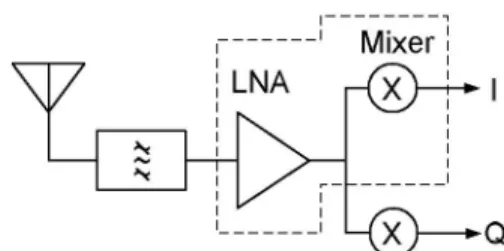
Fig. 1. The receiver front-circuit under consideration, including the LNAand mixer circuits in the dashed box.
II.DESIGN CONSIDERATION
The receiver front-end circuits under consideration include a low-noise amplifier (LNA) and a mixer, as
shown in Fig. 1, designed to operate in the 5-GHz ISM unlicensedfrequency band. Appliedtothesensornodes of short distance body-area networks, circuit performance requires no distinguished dynamic range. Acceptable trade-off between linearity and noise figure call for the condition that most power shall be assigned to the LNA
stagefor better overallperformance. A. LNA Circuit Design
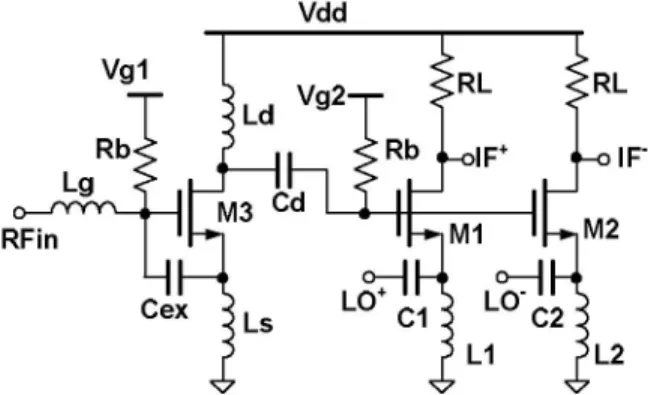
The proposed circuit schematic is as shown in Fig. 2. The circuit topology is chosen to allow a low supply voltage below 1V. The LNA stage is implemented by a
single transistor M3 biased in the saturation region to
provide sufficient signal gain. The biasing point and the transistor size are chosen to achieve good compromise
among those parameters of the gain, the minimum noise
figure, and thepowerconsumption.
The major issue is the stability condition. Inthe single MOS transistor amplifier, the electrical feedback due to
thegate-draincapacitance Cgdmustbe taken intoaccount
such that bilateral amplifier designis required. As can be
found, this causes the amplifier appear as conditionally
stable. The load stability circle typically cuts into the
upperregionof the Smithchart, whichmeans acapacitive
load is preferred to avoid instability. An inductive
load,
however, is necessary toconjugately
match the capacitiveoutputimpedanceatthe drainport. Inthepopularcascode
configuration [3], this is not an issueat all since the load
205
LO+iJL
I F
Fig. 2.Circuit schematicof the receiver front-end. TheLNA
circuit is a single-transistor amplifier (M3) with inductive
source degenerationto improve stability. The mixer circuit consists ofatransistorpair biasedinthe subthresholdregion for low powerconsumption.
w/ostablization w/i stablization
Fig. 3.Load stability circles of thesingle-transistor LNA at5GHzwith and without reactive stabilization.
impedance presented to the common-source configured transistor is low and capacitive. Not only the Miller feedback ofCgdisdecreased, but also the loadimpedance
sits in the stable region. To alleviate the issue, the transistor shall be stabilized by adding external
components without much degradation to noise
performance. As such, two reactive components, gate-source capacitor Cex and source inductor Ls, are added,
instead of resistive elements at the input or the output ports as in the conventional microwave amplifier design
[4]. Essentially the two components reduce the available
gain somewhat. The Ls also helps simultaneously noise and impedance matching [5]. Fig. 3 shows that the load
stability circles at 5GHz moves out of the Smith chart after stabilization. The gives room for impedance matching. Actually the stability condition shall be inspected over the frequency range from very low at
100MHzto 10GHz.
Fig. 4. LO differential signal is buffered by on-chip inverters. External bias-teesareused forDCblocking. Inbilateral amplifier design, the optimal sourceand the load impedance meet the condition of both simultaneous
conjugate
matching for matched gain [6]. The conditioncanbeexpressedas
US =
r,n
andFL=
FoX
(1)whereF,, and FOutarecharacterized with added Cex and Ls. As Ls already gives areal part to the input impedance, it
turns out that only Lg and Ld are used. Such simple
matching provides sufficient input return loss, or
Fs,
butnot the output return loss. Nevertheless this fully integrated LNA and mixer circuits can tolerate the unmatched loadimpedance withouttoo muchdegradation
tothegain level.
B. MixerCircuit Design
The mixer circuit is implemented by the transistor pair MI and M2 in thesingle-balanced configuration, asinFig. 2. It shallprovide frequency mixing and the required load impedance to LNA. Since the outputimpedance of M3 is high, the mixer is bettertoexhibithigh impedanceto ease
impedance matching. Consequently the RF signal is connectedto the gate ports of MI andM2, while the LO signal to the source ports. Frequency downconversion is different from that in the traditional Gilbert-cell circuit,
which, consisting of a transconductance stage and a
switching stage, utilizes current commutating. Even though the IF output current could be large, the transconductance stageis very power-consuming, and the DCbiasing current in operation will increase dramatically iftheswitchingtransistorsaredriven on-and-offbyalarge
LOvoltage swing.
To sustain low power consumption, the transistors are
biased in the subthresholdregion withoutlargeLOswing.
The exponential I/V characteristic of a MOS device carries out the nonlinearity that generates frequency mixing.Itcanbeexpressedas
(2)
Ids
=I, exp(
V)
' 77VT206
0 -2 -4 - -6 -8 n) -10 -12 -14 -16
Fig. 5.The micrograph of the fabricated low-power receiver front-end circuitin0.18um RF CMOStechnology.
where
3 4 5 6 7 8
Freq.(G Hz)
Fig. 6. Input returnloss of measured and simulated data.
Vgs =VGS+Vgs =VGS+(VRF-VLO)- (3)
The second-order nonlinear term in Eq. (2) results in the desired IF output current but no significant DC current because the LO swing is small due to the low node impedance at the source port. Although large LO swing improves the conversion gain, large voltage conversion gain is still available in this mixer if the output load resistance RL is chosen as large as possible. The largest value of RL is actually limited by the output parasitics. Combined with theoutputparasitic capacitance, thecorner
frequency in the low-passresponse mustbelarger than the
IF signal bandwidth. A few hundred ohms of RL
resistance gives sufficient gain andmorethan 10 MHz of
signalbandwidth. As the biascurrent isverylow, RLdoes
not causemuch DC voltage drop. The IFloadimpedance is typically up to the order of 10K ohms and causes no
significant loadingeffectontheRFresistance.
The LO differential signal is buffered by CMOS inverters, as shown in Fig. 4. The Cl-LI and C2-L2 sections form ahigh-pass filter andprovide DCblocking
between the inverters and the mixercorecircuit.
III.MEASUREMENT RESULTS
The front-end circuit is fabricated in 0. 18umRFCMOS
technology. The micrograph is shown in Fig. 5. The die size is 1.16 x 0.98
mm2,
including bonding pads.Measurements were conducted by chip-on-board setup.
DCpads arewire-bonded on aPCB board. All the signals
arethroughon-waferprobingwithaGSGprobetotheRF
input and GSGSG probes to the LO and IF ports. The differential IF signal is buffered by an on-board OP
amplifier of unit gain to convert to a single-ended form. The differential input impedance of the OP amplifier is chosen as 16 Kohms to emulate a high IF loading impedance. A 50-ohm resistor is added in seriesatthe OP
35 30 m - 25 CD 20 o X~15 au O 10 0 5 0 4 4.5 5 5.5 Freq.(GHz) 6 6.5 7
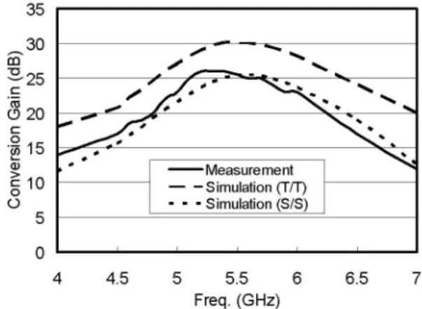
Fig. 7. Conversion gain of measured and simulated data, including bothcorner cases attypical/typical and slow/slow.
amplifier output for impedance matching to 50-ohm
measurement systems such that 6dB voltage gain shall be compensated in all the gainmeasurements.
The supply voltage Vdd is set as IV in the
measurements. The total DC power is about0.87mW, of which 0.7mW goes to the LNA stage and the rest to the mixer and the LO buffer. Even if both I/Q mixers are
fabricated, the total front-end power consumption is still within 1mW. The measured input return loss, plotted in Fig. 6, is centered at the simulated frequency around 5.5GHz with the magnitude better than 10dB but somewhatworsethan the simulated data. It is foundonthe Smith chart that the input impedance is lower than 50 ohms. This could be further improved by enlarging the
source inductor Ls to increase the real part under the
penalty of gain degradation. The measured conversion
gain is about 25dB, as shown in Fig. 7. It is about 5dB short as compared to the simulation. Further analysis
indicates that the result is approaching to the slow/slow
corner case. However, another uncertainty factor, the
modeling accuracy of MOS devices in the subthreshold
m co 0~ -2 -3 -4 -5 -6 -7 -8 -9 -10 4.8 5 5.2 5.4 5.6 5.8 6 6.2 Freq. (GHz) Fig. 8.Measured11P3.
region, might also contribute to this discrepancy. The measured NF and IIP3 are 12 dB and -6.5 dBm, respectively, as shown in Fig. 8 and Fig. 9. The noise figure is worse than the simulated data in both corner cases.
IV.CONCLUSION
A low-power receiver front-end circuit is designed and fabricated in 0.18um CMOS technology, with power consumption less than 1mW for applications of wireless
sensor networks. Measurement circuit performance is applicable to low duty-cycle data transmission. Although
the supply voltage is set as IV, itcan be further lowered down for the circuittopology chosen.
ACKNOWLEDGEMENT
The authors would like to acknowledge the Chip ImplementationCenter(CIC) for circuit fabrication support, andAnsoft Corp. fordesign support. This project is funded
18 16 -Measurement -Simulation(T/T) 14 - - -Simulation(S/S) m- 12 h U-z 10 8 6 4.8 5.0 5.2 5.4 5.6 5.8 6.0 6.2 Freq.(GHz)
Fig. 9. Measured noise figure (in solid line), higher than simulation data of bothcorner cases(in dashed lines).
jointly by National Science Council, Taiwan, ITRI/STC JRC at NCTU, and MediaTek Center at NCTU.
REFERENCES
[1] B. W. Cook, et al., "An Ultra-Low Power 2.4GHz RF Transceiver for Wireless Sensor Networks in 0.13um CMOS with400mV Supply and anIntegrated Passive RX
Front-End," IEEEISSCC Dig. Tech. Papers, pp. 370-371,
Feb. 2006.
[2] A. Molnar , et al., "An Ultra-Low Power 900 MHz RF Transceiver for Wireless Sensor Networks," IEEE CICC Dig. Tech. Papers, pp. 401-404, 2004.
[3] D. K. Shaeffer, and T. H. Lee, "A 1.5V, 1.5GHz CMOS Low Noise Amplifier," IEEE Journal of Solid-States Circuit, vol. 32,pp.745-759, May1997.
[4] G. Gonzalez, Microwave Transistor Amplifiers, 2nd Ed.,
PrenticeHall,1996.
[5] T. K.Nguyen, etal.,"CMOS Low-NoiseAmplifier Design Optimization Techniques,"IEEETrans. Microwave Theory Tech., vol. 52,no.5, pp.1433-1442,May 2004.
[6] D. M. Pozar, Microwave and RF Design of Wireless Systems,Chap. 6,J.Wiley&Sons,2004.
208