Study of GaN light-emitting diodes fabricated by laser lift-off technique
Chen-Fu Chu, Fang-I Lai, Jung-Tang Chu, Chang-Chin Yu, Chia-Feng Lin, Hao-Chung Kuo, and S. C. Wang
Citation: Journal of Applied Physics 95, 3916 (2004); doi: 10.1063/1.1651338
View online: http://dx.doi.org/10.1063/1.1651338
View Table of Contents: http://scitation.aip.org/content/aip/journal/jap/95/8?ver=pdfcov Published by the AIP Publishing
Articles you may be interested in
Improvement of light extraction from GaN-based thin-film light-emitting diodes by patterning undoped GaN using modified laser lift-off
Appl. Phys. Lett. 92, 141104 (2008); 10.1063/1.2906632
Dichromatic InGaN-based white light emitting diodes by using laser lift-off and wafer-bonding schemes Appl. Phys. Lett. 90, 161115 (2007); 10.1063/1.2722672
Vertical AlGaN deep ultraviolet light emitting diode emitting at 322 nm fabricated by the laser lift-off technique Appl. Phys. Lett. 89, 261114 (2006); 10.1063/1.2424668
Photonic crystal laser lift-off GaN light-emitting diodes Appl. Phys. Lett. 88, 133514 (2006); 10.1063/1.2189159
Fabrication of thin-film InGaN light-emitting diode membranes by laser lift-off Appl. Phys. Lett. 75, 1360 (1999); 10.1063/1.124693
LLO-LEDs on the sapphire substrate. High operation current up to 400 mA for the LLO-LEDs on Cu was also demonstrated. Based on the emission wavelength shift with the operating current data, the LLO-LEDs on Cu show an estimated improvement of heat dissipation capacities by nearly four times over the light-emitting devices on sapphire substrate. The LLO process should be applicable to other GaN-based LEDs in particular for those high light output power and high operation current devices. © 2004 American Institute of Physics. 关DOI: 10.1063/1.1651338兴
I. INTRODUCTION
GaN-based wide-band-gap semiconductors are widely used for optoelectronic devices, such as blue light-emitting diodes 共LEDs兲 and laser diodes 共LDs兲. These devices were grown heteroepitaxially onto dissimilar substrates, such as sapphire and SiC, because of difficulties in the growth of bulk GaN. The sapphire is the most commonly used substrate because of its relatively low cost. However, due to the poor electrical and thermal conductivity of sapphire substrate, the device process steps are relatively complicated compared with other compound semiconductor devices. Therefore, GaN optoelectronics devices, fabricated on an electrically and thermally conducting substrate by separating sapphire substrate, are most desirable. The separation of hydride va-por phase epitaxy-grown 2 in. GaN wafer from the sapphire substrate was demonstrated1by using the laser lift-off共LLO兲 technique. The pulsed high-power UV laser of the third har-monic of a Q-switched Nd:YAG laser with a 355 nm wave-length was used to irradiate through the transparent sapphire substrate to lift off the GaN film. The physical process re-sponsible for the lift off appears to be dominated by the rapid thermal decomposition of GaN near the sapphire interface. Recently, the LLO technique has been used to fabricate free-standing InGaN LEDs and LDs.2– 4These include p-side up GaN LEDs with Ti/Al as p and n contact, the p-side down InxGa1⫺xN LEDs on Si substrates with Pd–In as the p-GaN contact and bonding metal, and p-side up InGaN laser diodes on copper substrates. However, in Refs. 2– 4, different p-GaN contact metals were used for either the conventional LEDs and LLO-LEDs or the LLO-LEDs were mounted in the same transferred substrate, which makes the performance comparison relatively difficult. In our recently report,5 we compared the performance of p-side up and p-side down
LLO-LEDs on a copper substrate with the same p-GaN con-tact metals, and demonstrated a superior performance of the p-side down configuration of GaN LEDs over the p-side up LEDs. The result suggests that the p-side down LLO-LEDs can enhance the light output power, operate at high current, and increase the heat capacity of GaN-based LEDs. In this article, we report the detail investigation results of the GaN LLO process and the establishment of GaN LLO conditions, the demonstration of the GaN light emitting devices with high current operation.
II. LASER LIFT-OFF SETUP AND PROCESS CONDITIONS
Figure 1 shows the schematic diagram of the setup for the conducting LLO experiment. A KrF excimer laser
共Lambda Physick LPX210兲 at wavelength of ⫽248 nm
with pulse width of 25 ns was used for LLO. The laser out-put energy can be varied from 10 nJ to 25 mJ. The laser beam is reshaped and homogenized using a special optical system to form a highly uniform 关⫾5% root-mean-square
共rms兲兴 beam profile of 12⫻12 mm2
after the mask plane. A beam splitter then splits the laser beam into a LLO beam and a monitor beam. The LLO processing beam passed through a projection system of 10⫻ with a 0.2 numerical aperture, and then focuses onto the sample with a square spot size of 1.2
⫻1.2 mm2
. The monitor beam is incident on a beam analyzer for real-time monitoring of the laser beam quality. The samples were placed on the top of working station which can be moved 1.2 mm step by step to scan a typical sample size of 2 cm⫻2 cm by using the computer-controlled stepper mo-tor. The charge coupled device camera was used to in situ monitor the LLO process. For establishing LLO conditions for GaN, the effect of laser fluence on the ablation of GaN materials under a different environment was investigated first. A bare undoped GaN sample of 14.9m thickness was irradiated with the laser beam under two pressure conditions: a兲Author to whom correspondence should be addressed; electronic mail:
3916
0021-8979/2004/95(8)/3916/7/$22.00 © 2004 American Institute of Physics
One atmosphere pressure and 10⫺3Torr. The laser fluence was varied from 0.2 to 1.0 J/cm2 at a constant number of pulses. The laser irradiation causes the decomposition of GaN into gaseous nitrogen and gallium droplets, following the equation:
GaN⇔Ga⫹1 2N2共g兲.
The GaN sample after laser irradiation tends to show some material residues, such as Ga and Ga oxide. These residues were then cleaned up by a dilute acid solution, such as HCl or H2SO4/H2O2, before the measurement of the etched depth.
Figure 2 shows the rate of removable of GaN, or etching rate, as a function of laser fluence for the two different pres-sure conditions. The etching rates increase with increasing laser fluence under both conditions. At the incident laser flu-ence of 1.0 J/cm2, the etching rate was about 35 nm/pulse, and 60 nm/pulse for one atmosphere pressure and 10⫺3Torr, respectively.
According to the chemical kinetic theory,6 a system in stable chemical equilibrium subjected to the influence of an exterior force tends to cause a variation in its pressure. For a GaN sample irradiated under the low pressure of 10⫺3Torr, which is lower compared with the one atmosphere condition,
the decomposition rate of GaN should be higher than that of the sample placed in one atmosphere condition. Thus, a higher etching rate was obtained in a low-pressure condition. Based on the laser etching of GaN sample, we obtained the threshold laser fluence for ablation of GaN surface to be about 0.3 J/cm2.
From the etching rate and the incident laser fluence re-lationship, the GaN material absorption coefficient at a KrF laser wavelength can also be estimated based on the widely accepted formula of Beer’s law:7
d⫽
冉
1␣
冊
ln冉
Ei
Eth
冊
,where d is the etched depth per pulse, ␣ is the absorption coefficient, Ei is the incident laser fluence, and Eth is the threshold laser fluence for material removal. By plotting the etching rate versus logarithm of incident fluence Ei, we
ob-tained an absorption coefficient of about 2.5(⫾2.0)
⫻105cm⫺1 from the slopes of the plot. This value is in agreement with the reported data for GaN obtained from the optical measurement method.8
The dependence of the etched depth on the numbers of pulses at a higher laser fluence of 3.75 J/cm2was also inves-tigated to establish the optional LLO condition. The sample was etched under an atmosphere condition with a different number of pulses. Figure 3 shows the etched depths as a function of pulse numbers. The etched depth increases lin-early with the numbers of pulses. This dependence is similar to the reported elsewhere.9From these data, the higher etch-ing rate, as high as 82 nm/pulse, was obtained at a higher laser fluence. Figure 4 shows a scanning electro microscopy
共SEM兲 picture of the etched sidewall. The etched surface
morphology was also obtained by atomic force microscopy
共AFM兲 measurement in contact mode operation with a scan
area of 5 m2. Figure 5 shows the typical AFM images for the samples under these two different conditions. The rms roughness of the surface morphology is around 4 –14 nm for the sample processing in the atmosphere pressure condition, and around 30–36 nm for the sample processing under a low pressure condition. These results show that the
decomposi-FIG. 1. The schematic diagram of laser etching and LLO process setup.
FIG. 2. The rate of removable of GaN or etching rate as a function of laser fluence for the two different pressure conditions.
FIG. 3. The etching rate as a function of pulse numbers at the laser fluence of 3.75 J/cm2under the atmosphere condition.
3917
J. Appl. Phys., Vol. 95, No. 8, 15 April 2004 Chuet al.
tion of GaN material under the atmosphere pressure condi-tion has a relatively better surface morphology. Therefore, the GaN LLO was conducted process under the atmosphere environment.
The relation between the decomposition temperature at the irradiated surface T, and the absorbed irradiation Ia for
material heating can be expressed as:10 T共t兲⫽Ia
K
冑
共1⫺R兲,where ⫽2(Dt)1/2 is the diffusion length, and the thermal diffusivity D⫽K/Cp, K is the thermal conductivity, Cp is
the heat capacity,is density, t is the pulse duration, and R is the reflectivity. For GaN material, the decomposition tem-perature 共T兲 is about 900 °C–1000 °C,11–13K⫽1.3 W/cm K, Cp⫽9.75 cal/mol K, ⫽6.11 g/cm
3
, t⫽25 ns, and R⫽0.3.14 –16 Using these values, the absorbed laser fluence required for decomposition of GaN is about 0.3 J/cm2, which is in agreement with the experiment value.
The LLO process was first conducted using an undoped GaN sample grown on a sapphire substrate. The back side of sapphire was first polished by various sizes of diamond paste ranging from 3m to 1m, then cut to a sample size of 1 cm⫻1 cm. The sample was bonded to a Si wafer using cy-anoacrylate (C6H7NO2)-based ester adhesive forming a sapphire/u-GaN/epoxy/Si structure. The sample was placed
on the top of the workstation in air. Figure 6 shows the LLO process sequence for the fabrication of freestanding undoped GaN. The pulsed KrF excimer laser with a spot size of 1.2 mm⫻1.2 mm was directed through the back side of the pol-ished transparent sapphire substrate. Since the attenuation of the KrF excimer laser through the 0.5 mm thick sapphire substrate is approximately 20%–30% 共Ref. 17兲 and the re-flection of the interface of sapphire/GaN at 248 nm is ap-proximately 20%,9 the incident laser fluence was set to a value of 0.6 J/cm2, corresponding to a laser fluence of about 0.3 J/cm2 at the interface. With the incident fluence of 0.6 J/cm2, the metallic silver color with size of 1.2 mm⫻1.2 mm clearly appeared in the interface of GaN and sapphire with the ejection of some dustlike particles from the edge of sample, indicating the decomposition of the Ga interfacial layer between GaN and sapphire. By heating the irradiated samples at the Ga melting point of 30 °C, the GaN film was then easily separated from the sapphire substrate and trans-ferred onto the Si supported carrier. The metallic Ga residues were removed to complete the LLO process.
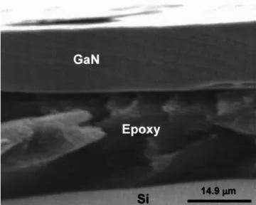
The LLO GaN sample was characterized by using scan-ning electron microscopy共SEM兲, AFM, x-ray rocking curve
共XRC兲, and photoluminescence 共PL兲 spectrum
measure-ments. Figure 7 shows a typical cross-sectional SEM micro-graph of the LLO GaN sample. The structure of GaN/ epoxy/Si was clearly depicted. The thickness of LLO-GaN
FIG. 4. The SEM picture of the etched sidewall.
FIG. 5. The typical AFM images for the samples under these two different conditions:共a兲 The atmosphere condition and 共b兲 low pressure of 10⫺3Torr.
FIG. 7. A typical cross-sectional SEM micrograph of 14.9-m-thick un-doped sample.
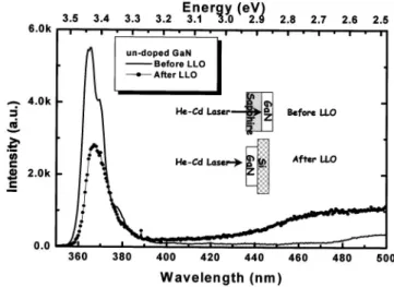
film was measured around the value of 14.9 m indicating the reduction in thickness is relatively small after the LLO process. Figure 8 shows typical AFM images of the LLO-GaN film surface. Uneven and whiskerlike micropole struc-tures were formed as the result of the lift-off process. The rms values of the GaN surface roughness were around 12 nm, which is consistent with the results of the GaN-etched surface for the sample etching in the atmosphere pressure condition. The rms value of 12 nm compared to the value of 0.3 nm for the sample before LLO was larger due to the thermal decomposition which occurred in the interface of GaN and sapphire. Figure 9 shows the XRC spectrum of the GaN sample before and after lift off. The full width at half maximum共FWHM兲 value of the LLO film is about 528 arcs, which is slightly larger than that of the regular GaN film of 412 arcs. The increase in the FWHM of the rocking curve maybe due to the thermally induced lattice disorder carried by the laser irradiation.18 Figure 10 shows the PL spectrum of the GaN sample before and after the LLO process. The emission peak of LLO-GaN is at 364 nm, which is slightly redshifted compared to the emission peak before LLO. A
similar redshift was reported previously18 and attributed to the induced localized defects in the GaN/sapphire interface caused by the LLO process.
III. FABRICATION OF LASER-LIFT OFF-GaN LIGHT-EMITTING DEVICES
The LLO process was used to fabricate freestanding GaN LED on copper substrate. The copper substrate was selected for its good electrical and high thermal conductivity.19The LED wafer structure was grown by met-alorganic chemical vapor deposition on共1000兲 sapphire sub-strate. The LED structure consists of a 25-nm-thick GaN low-temperature buffer layer, a 1.5-m-thick undoped u-GaN layer, a 1.5-m-thick highly conductive n-type GaN layer, a multiple quantum well 共MQW兲 region consisting of five periods u-GaN 2/5-nm-thick InGaN/GaN MQWs, and a 0.3-m-thick p-type GaN layer.
The fabrication process of the LLO-LEDs on a Cu sub-strate is shown in Figs. 11共a兲–11共h兲. The process involves the LLO of the LED wafer process first followed by the
FIG. 8. A typical AFM image of the LLO undoped GaN film surface.
FIG. 9. The XRC spectrum of the undoped GaN before and after LLO.
FIG. 10. The PL spectrum of the undoped GaN before and after LLO.
FIG. 11. The schematic diagram of the fabrication process for the LLO-LEDs on Cu substrate:共a兲 p-type metal deposition, 共b兲 Cu substrate bond-ing, 共c兲 laser processing. 共d兲 separation, 共e兲 etching of u-GaN layer, 共f兲 300-m-square mesa formation and device isolation, 共g兲 n-type contact deposition, and共h兲 freestanding p-side down LLO-LEDs on Cu.
3919
J. Appl. Phys., Vol. 95, No. 8, 15 April 2004 Chuet al.
fabrication of LEDs on a Cu substrate. The GaN LED wafer sample with size of about 1 cm⫻1 cm was deposited with p-contact metallization using Ni/Pd/Au 共20 nm/20 nm/100 nm兲20 as the p-GaN contact and the back side of sapphire substrate was polished. Then, the sample was annealed in oxygen at 550 °C for 5 min first to form the p-type ohmic contact. The sample was then bonded onto an indium-coated Cu substrate at 200 °C to form a structure of sapphire/GaN LED/Ni/Pd/Au/In/Cu. In this process, the Ni/Pd/Au p-type contact also serves as the bonding material without using any other bonding substance. The bonded structure was then sub-jected to the LLO process as described earlier to form an u-GaN/n-GaN/MQW/ p-GaN structure on a Cu substrate. Then, the u-GaN was etched away by inductively coupled plasma reactive ion etching共ICP/RIE兲 to expose the n-GaN layer. The typical rough and uneven surface of the u-GaN after the LLO process was also evened out by the ICP etch-ing process to form a relatively smooth surface for the n-contact formation. Then, a square mesa of 300 m⫻300
m was created by ICP/RIE for current isolation purposes. Finally, a Ti/Al with a diameter of 100m circular pad was deposited as the n-type contact on the center of square mesa without any other semitransparent contact layer. The com-pleted top and side views of the LLO-LEDs on Cu are shown in Fig. 12. It has a low resistivity n-GaN top layer which facilitates better current spreading21without the need for an additional semitransparent ohmic contact metallization typi-cal of the regular LEDs on sapphire substrate. The LLO-LED on Cu has a lager emission area of about 90% compared to the entire mesa range 共300m⫻300m兲.
IV. PERFORMANCE OF LASER LIFT OFF-LIGHT-EMITTING DIODES
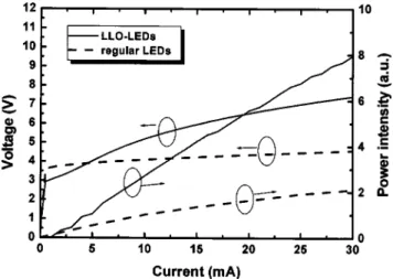
In order to compare the performance of LLO-LEDs on Cu with regular GaN LEDs on a sapphire substrate, regular GaN LEDs on sapphire were also fabricated using the same wafer structure. Figure 13 shows the scheme of the regular LEDs, which has a Ni semitransparent layer and the same metal p- and n-contact metallization as the LLO-LEDs. The regular GaN LEDs on sapphire has an emission area of about 50% compared to the entire mesa range共300m⫻300m兲. Figure 14 shows the light output power–current–voltage
(L – I – V) characteristics under low current continuous-wave
共cw兲 operation conditions for the LLO-LEDs on Cu, and the
regular LEDs on sapphire. The voltage at 20 mA is about 4.2 V for the regular LEDs on sapphire and 6.5 V for the LLO-LEDs on Cu. The higher operating voltage of the LLO-LLO-LEDs on Cu could be caused by the degradation in the p contact after the bonding process. Nevertheless, the light output power of the LLO-LEDs on Cu was about four times larger than that of regular LEDs on sapphire at the operated current of 20 mA. The increase in the output power could be due to several factors. First, the effect of the light-emitting area of the LLO-LEDs on Cu is about 1.8 times larger than that of the regular LEDs on sapphire. Second, the GaN/Ni interface has a reflectivity of about 37% 共Refs. 22–24兲 at a LED wavelength of 470 nm which is higher than that of the GaN/ sapphire interface of 2%. The light output has about a 34% enhancement for the LEDs on Cu. Third, the LLO-LEDs on Cu with n-side up configuration without a semi-transparent metal has about a 1.6 times higher light output power than that of the regular GaN LEDs on sapphire due to no light absorption by the semitransparent contact metal. Fi-nally, according to Ref. 21, the GaN LEDs with a n-side up configuration tend to have higher light output power com-pared to the regular GaN LEDs on sapphire due to no current
FIG. 12. The completed top and side view of the LLO-LEDs on Cu.
FIG. 13. The typical top and side views of the regular GaN LED on sap-phire substrate.
FIG. 14. The L – I – V characteristics for the LLO-LEDs on Cu, and the regular LEDs on sapphire.
crowding effect. Furthermore, the LLO-LEDs on Cu require no additional semitransparent metal layers, which simplifies the fabrication process.
Figure 15 shows the comparison of the light output power–current (L – I) characteristics for the LLO-LEDs on Cu, and the regular LEDs on sapphire under high current cw operation conditions. The light output power of the regular LEDs on sapphire increased with increasing current up to about 225 mA, saturated at around 225 mA, and gradually degraded when the operation current exceeded 270 mA. On the other hand, the light output power of the LLO-LEDs on Cu increased with increasing current up to about 225 mA and maintained the same power level after exceeding 225 mA, and was still operational up to 400 mA; suggesting superior heat dissipation with the Cu substrate and also allowing higher current operation with higher light output.
Figure 16 shows the variation of LED emission peak wavelength for the regular LEDs on sapphire and the LLO-LEDs on Cu under high current cw operation conditions. The peak wavelength of regular LEDs on sapphire showed a
rela-tively larger redshift of about 9 nm from a low current of 20 mA to a high current of 250 mA. While, the peak wavelength of the LLO-LEDs on Cu showed only a slight redshift of only about 2–3 nm in the same current range. Using the reported wavelength drift⌬ with temperature ⌬Tjvalue of
0.06 nm/°C 共Ref. 25兲 for a GaN MQW LED, we estimated the junction temperature increase based on the wavelength shift of the regular LEDs on sapphire to be about 150 °C corresponding to a temperature increase rate of 0.65 °C/mA. While for the LLO-LEDs on Cu, the junction temperature increase is about 40 °C corresponding to a temperature in-crease rate of 0.17 °C/mA which is about four times lower than that of the regular LEDs on sapphire. These results in-dicate the LLO-LEDs on a copper substrate do provide a much better heat dissipation capability than the regular LEDs on sapphire substrate, and allows higher current operation.
V. CONCLUSION
In conclusion, we have fabricated GaN LLO-LEDs on Cu by using a KrF excimer laser at 248 nm with the laser fluence of 0.6 J/cm2to separate the GaN LED wafer structure from the sapphire substrate first and then transfer the LLO-LED wafer structure onto a Cu substrate. The LLO-LLO-LEDs on Cu showed a substantial increase in light output power of about four fold over that of the regular LEDs fabricated on the sapphire without degradation in the output light intensity. From the wavelength shift with the operating current data, the LLO-LEDs on Cu showed a four times greater estimated improvement of in heating dissipation capacity over the regular LEDs on sapphire. The LLO-LEDs on Cu with a p-side down configuration in particular should be suitable for high light output power, and high operation current GaN-based optoelectronic devices.
ACKNOWLEDGMENTS
This work was supported in part by the National Science Council of Republic of China共ROC兲 in Taiwan under Con-tract No. NSC 92-2215-E-009-015 and by the Academic Ex-cellence Program of the Ministry of Education of ROC under Contract No. 88-FA06-AB.
1
M. K. Kelly, O. Ambacher, B. Dahlheimer, G. Groos, R. Dimitrov, H. Angerer, and M. Stutzmann, Appl. Phys. Lett. 69, 1749共1996兲.
2W. S. Wong, T. Sands, N. W. Cheung, M. Kneissl, D. P. Bour, P. Mei, L.
T. Romano, and N. M. Johnson, Appl. Phys. Lett. 75, 1360共1999兲.
3
W. S. Wong, T. Sands, N. W. Cheung, M. Kneissl, D. P. Bour, P. Mei, L. T. Romano, and N. M. Johnson, Appl. Phys. Lett. 77, 2822共2000兲.
4M. Kneissl, W. S. Wong, D. W. Treat, M. Teepe, N. Miyashita, and N. M.
Johnson, Phys. Status Solidi A 188, 23共2001兲.
5C. F. Chu, C. C. Yu, H. C. Cheng, C. F. Lin, and S. C. Wang, Jpn. J. Appl.
Phys., Part 2 42, L417共2003兲.
6F. Battaglia and T. F. George, Fundamentals in Chemical Physics共Kluwer,
Boston, 1998兲.
7L. Migliore, Laser Materials Processing 共Markcel Dekker, New York,
1996兲.
8
J. F. Muth, J. H. Lee, I. K. Shmagin, R. M. Kolbas, H. C. Casey, Jr., B. P. Keller, U. K. Mishra, and S. P. DenBaars, Appl. Phys. Lett. 71, 2572
共1997兲.
9H. Chen, R. D. Vispute, V. Talyansky, R. Enck, S. B. Ogale, T. Dahmas, S.
Choopun, R. P. Sharma, T. Venkatesan, A. A. Iliadis, L. G. Salamanca-Riba, and K. A. Jones, Mater. Res. Soc. Symp. Proc. 482, 1015共1998兲.
10M. Von Allmen and A. Blastter, Laser-Beam Interactions with Materials, FIG. 15. Comparison of the L – I characteristics for the LLO-LEDs on Cu,
and the regular LEDs on sapphire under high current cw operation condi-tions.
FIG. 16. Comparison of the peak wavelengths under high current cw opera-tion condiopera-tions for the LLO-LEDs on Cu, and regular LEDs on sapphire.
3921
J. Appl. Phys., Vol. 95, No. 8, 15 April 2004 Chuet al.