國
立
交
通
大
學
電機資訊學院 電信學程
碩
士
論
文
一低複雜度無線區域網路Viterbi解碼器
之設計與實作
Design and Implementation of a
Low-complexity WLAN Viterbi decoder
研 究 生:劉昌明
一低複雜度無線區域網路Viterbi解碼器
之設計與實作
Design and Implementation of a
Low-complexity WLAN Viterbi decoder
研 究 生:劉昌明 Student:Chang-Ming Liu
指導教授:吳文榕 Advisor:W.R. Wu
國 立 交 通 大 學
電機資訊學院 電信學程
碩 士 論 文
A Thesis
Submitted to Degree Program of Electrical Engineering and Computer Science
College of Electrical Engineering and Computer Science
National Chiao Tung University
in Partial Fulfillment of the Requirements
for the Degree of
Master of Science
in
Communication Engineering
June 2004
Hsinchu, Taiwan, Republic of China
一低複雜度無線區域網路Viterbi解碼器
之設計與實作
學生: 劉昌明 指導教授: 吳文榕 教授
國立交通大學電機資訊學院 電信學程﹙研究所﹚碩士班
摘
要
近幾年來無線區域網路被廣範使用並快速的普及, 維特比 (Viterbi) 解碼器是大家 耳熟能詳的解碼方法,它在基頻接收器中扮演非常重要的角色, 維特比演算法可以 採用軟決策(soft decision)或是硬決策(hard decision)的做法來實現, 軟決策的做法 可以得到較佳的解碼效能但是需要較複雜的運算能力, 在某些無線網路的應用中 並不嚴苛要求效能,此時硬決策便可以滿足系統的要求。在本論文中,我們考慮設 計並實現一個無線網路中使用硬決策的維特比解碼器,我們提出一個加權硬決策 的做法,此做法可以有效提升硬決策維特比解碼器的效能並且享有硬決策的簡易 運算的優點,另外我們使用預測追蹤法來有效降低記憶體使用頻率, 如此可降低約
Design and Implementation of a
Low-complexity WLAN Viterbi Decoder
Student: Chang-Ming Liu Advisors:Prof. Wen-Rong Wu
Degree Program of Electrical Engineering
Computer Science
National Chiao Tung University
ABSTRACT
The wireless local area network (WLAN) has been widely used in recent years. The Viterbi decoder, a well-known decoding scheme, plays an important role in the baseband receiver. The Viterbi algorithm can be implemented as soft-decision or hard-decision. The soft-decision Viterbi algorithm has better performance but requires higher computational complexity. In some WLAN applications, the performance requirement is not stringent. In this case, the hard-decision decoding algorithm can be sufficient. In this thesis, we consider the design and implementation of a
hard-decision WLAN Viterbi decoder. We propose a hard-hard-decision weighting scheme that can effectively enhance the conventional hard-decision Viterbi decoder while remains the inherent low complexity property. We also use a trace back prediction method that can reduce the memory access frequency during the trace back operation. This can reduce the power consumption of the whole decoder up to 20%. Finally, we use VHDL to model the designed decoder and implement it using an FPGA.
Acknowledgement
At first, I would like to acknowledge to my advisor, Dr. Wen-Rong Wu, for his encouragement and give me the guidelines during my graduate study. I also
appreciate with my friend Ming and Leory for the discussion and help me to build up the simulation environment. Finally, I want to thanks my wife for her kindly support and encouragement.
Contents
Chinese Abstract ... i English Abstract... ii Acknowledgement ... iii Contends ... iv List of Figures ... vi Chapter 1 Introduction 1-1 Motivation ...11-2 Previous work review ...1
1-3 Our approach ...2
1-4 Outlines...3
Chapter 2 WLAN system description ...4
2-1 WLAN introduction...4
2-2 IEEE 802.11a standard ...5
2-3 Coded OFDM systems ...10
Chapter 3 The Viterbi decoder design ...11
3-1 Viterbi algorithm ...11
3-2 Hard decision and soft decision...16
3-3 Hard decision weighting...18
3-4 Viterbi decoder with receiver diversity ...27
3-6 Memory management and adaptive tracing back ...31
Chapter4 Low power Viterbi decoder implement...38
4-1 Design and implementation flow...38
4-2 Implementation of Viterbi algorithm...39
4-3 Over flow consideration ...41
4-5 Function simulation, gate level simulation and power verification...46 Chapter5 Conclusions ...50 References ...51
List of Figures
Figure 2.1 Convolutional encoder (k=7) ... 6
Figure 2.2 IEEE 802.11a baseband system architecture...7
Figure 2.3 Data stream from transmitter to receiver (using 16QAM modulation)...9
Figure 3.1 Convolutional encoder (rate ½ k=3 m=2) ...11
Figure 3.2 (a) Viterbi decoder trellis diagram (1)...13
Figure 3.2 (b) Viterbi decoder trellis diagram (2)...13
Figure 3.2 (b) Viterbi decoder trellis diagram (3)...14
Figure 3.3 Viterbi decoder trace back path ... 14
Figure 3.4 (a) QPSK hard decision plane ...16
Figure 3.4 (b) Trellis section, when data input as (1,1) ...16
Figure 3.5 (a) QPSK 2-bit (4-level) soft decision plane ... 16
Figure 3.5 (b) Trellis section, when data input as (3,1) ...16
Figure 3.6 BPSK decision plane ... 17
Figure 3.7 Received symbol distribution (1). ...19
Figure 3.8 Received symbol distribution (2) ...20
Figure 3.9 The cost function vs. threshold ...21
Figure 3.10 BER vs. threshold and weight ...22
Figure 3.11 Received symbol distribution (3) ...23
Figure 3.12 Cost function value vs. γ2 for two-weight algorithm ...24
Figure 3.13 Cost function value vs. γ1 for two-weight algorithm (γ2=0.77) ...25
Figure 3.14 Hard decision weighting improve performance ... 25
Figure 3.15 Antenna selection diversity ...27
Figure 3.16 Antenna combing diversity ...28
Figure 3.17 Comparison between NORMAL, OMRC and VMRC ...29
Figure 3.18 Comparison between NORMAL, OMRC2, OMRC3, OMRC4, VMRC2, VMRC3 and VMRC4 ...30
Figure 3.19 One-pointer trace back method ...32
Figure 3.20 Viterbi decoder trace back path in memory bank... 33
Figure 3.21 Write data to recode all possible trace... 34
Figure 3.22 Trace forward skip trace back scheme ... 34
Figure 3.23 Trace forward hit rate with different SNR ... 35
Figure 3.25 Minimum-transition trace back operation scheme ...37
Figure 4.1 Design and implementation flow... 38
Figure 4.2 802.11a channel decoder architecture ... 39
Figure 4.3 802.11a Viterbi decoder design block diagram... 40
Figure 4.4 802.11a trellis diagram ... 41
Figure 4.5 Structure of adder comparator selective unit (ACSU) ... 42
Figure 4.6 Modulo comparison of normalized metrics... 43
Figure 4.7(a) Radix-2 trellis... 44
Figure 4.7(b) Radix-4 trellis ... 44
Figure 4.7(c) Radix-2 one node structure ...44
Figure 4.7(d) Radix-4 one node structure ... 45
Figure 4.8 Prime power shows Viterbi decoder power consumption ...47
Figure 4.9 (a) Viterbi decoder input and output signal waveform ...47
Figure 4.9 (b) Viterbi decoder internal signal waveform ... 48
Figure 4.10 Prime power shows Viterbi decoder power distribution ... 49
Chaper
1
Introduction
1-1 Motivation
Convolution coding [11] is widely used in wireless communication system, such like satellite communication, broadcast systems, and WLAN. The Viterbi algorithm is a well-known algorithm for maximum likelihood convolution decoding.
Unfortunately, the Viterbi decoder requires high computational complexity. When it is implemented, a complex logic circuit will result. Conventionally, the Viterbi decoder can provide two kinds of solutions; one is called hard decision and the other soft decision. The soft decision Viterbi algorithm can give better decoding result; however, its complexity is higher. It depends on the application where the hard or soft decision Viterbi algorithm will be called for. In some scenarios, we need a low-cost solution rather high performance. In others, we may need high performance disregard its cost. We have to take cost, performance, and power consumption into account in order to make a best decision. In this thesis, we will focus on the hard decision Viterbi decoder and develop and implement a low complexity yet low power Viterbi decoder.
1-2 Previous work review
The Viterbi decoder use an efficient architecture to perform the maximum likelihood sequence estimation (MLSE) on the receive data. It keeps track of the path
metric (PM), which is an accumulation of the branchmetric (BM), and selects the
path with the lowest PM as its output. The difference between the soft-decision and hard-decision Viterbi algorithm lies in that the different criteria used in the BM calculation. The soft-decision approach first quantizes the input signal with multiple bits and uses the Euclidean distance as the BM criterion. On the other hand, the hard-decision approach quantizes the input signal with one bit and uses the Hamming distance as the BM calculation criterion. It is known that the Euclidean distance is more accurate then the Hamming distance reflecting the likelihood of a particular bit sequence. As a result, the performance of the soft-decision approach is better.
However, it’s requires higher computational complexity. The difference will become even more apparent when the Viterbi decoder is implemented. We require only
“XOR” logic operations to calculate the Hamming distance, while we require multiplication operations to calculate Euclidean distance.
For OFDM systems, transmit bits are spread all over different tones. As a result, the signal to noise ratio (SNR) may be different for all bits. The performance of soft-decision Viterbi algorithm can be further enhanced if we take channel state
information (CSI) into account. In this approach, the BM for each transmit bit is weighted according to the SNR in the corresponding tone [16]. The soft-decision Viterbit algorithm with CSI needs to estimate the signal power and noise power. This may complicate the receiver design and real-world implementation. As mentioned, in some scenarios, a higher performance Viterbi recoder may not be necessary. The issue is the implementation cost. In this case, the hard-decision Viterbi algorithm will be more suitable.
There are two well know structures for the Viterbi decoder implementation. The first one is called the register exchange method (REM) [14] and the other one is called the track back method (TBM). Implementation of the REM is simpler and its
throughput is higher. The disadvantage is that it requires many registers to store survive bits and these bits must be read and rewritten for each data cycle [12] [13]. Thus, this method will require more chip area and more power consumption. The TBM, on the other hand, stores the survivor bits in memory and then traces back the path history for decoding. Since the area and power consumption of memory is much lower than those of the register, the TBM is used more often. The disadvantage of the TBM is the memory control is somewhat more complicated.
In the TBM, the memory transactions contribute more than half the total power dissipation [3]. Thus, if we want to further reduce the power consumption, how to reduce the memory transaction times is the key issue.
1-3 Our approach
This thesis considers a low-cost and low-power hard decision Viterbi decoder design that is applied to IEEE802.11a WLAN system. As mentioned, although the hard-decision approach is simple, its performance is not as good as the soft-decision approach. In this thesis, we propose a new method called “hard-decision weighting” to improve the decoding performance. The proposed algorithm has a simple operation,
result, the power consumption can be further reduced. Combing with our decision weighting, we can then obtain a high performance yet low power hard-decision Viterbi decoder design.
1-4 Outlines
In this thesis, we will design and implement the hard-decision Viterbi decoder base on the IEEE 802.11a WLAN standard. The encoding rate is ½, the constraint
length is 7, and the generator polynomials G1=1388 and G2=1718 (see Figure 2.1).
The organization of the thesis is described as follows. Chapter 2 briefly describes the IEEE802.11a WLAN system. Chapter 3 describes various Viterbi algorithms
including the hard-decision, soft-decision, and soft-decision with CSI schemes. We also described the proposed hard-decision weighting and modify adaptive trace back, besides, we discuss about Viterbi decoder with receiver diversity. Chapter 4 addresses implementation issues. In this chapter, we discuss our implementation flow, specific functional blocks, function simulations, and gate level simulations. We also use the FPGA (Xilinx Vertix-2) implementation to evaluate our design and Prime power for power analysis. Chapter5 describes conclusions and future works.
Chapter 2
WLAN system description
2-1 WLAN introduction
In 1997, IEEE released IEEE 802.11 standard. Two year later, IEEE announced 802.11b wireless local area network (WLAN). The initial standard provides 1 Mbps and 2 Mbps transmission rate. Since the data rate is not high enough for many applications, the WLAN was not popular at that time. Due to the strong demand for higher data rates, IEEE 802.11b then incorporates the complementary code keying (CCK) scheme in direct sequence spread spectrum (DSSS) and increases the data rate up to 5.5 and 11Mbps. Since then, the WLAN usage experiences a rapid growth.
Recently, more and more applications are explored in the Internet. These include E-mail, VOIP, interactive games, and multimedia on demand (MOD). The bandwidth requirement becomes larger and larger and 802.11b seems not able to satisfy the requirement now. In the recent years, a high efficient transmission scheme called orthogonal frequency division multiplexing (OFDM) has been developed. In order to boost the data rate in the WLAN, IEEE then announced two standards 802.11a and 802.11g in 1999 and 2003, respectively. Both standards use the OFDM technique operated in 5-GHz and 2.4-GHz radio band. The data rate for both systems can up to 54Mbps.
Many manufacturers provide 802.11/a/b/g combined solution for WLAN
application now. The WLAN technology has been becoming the major stream in the notebook communication. We will introduce the 802.11a standard and coded OFDM system in the following sections.
2-2 IEEE 802.11a standard
IEEE802.11a standard adopts the OFDM modulation for high transmutation data rate in the 5GHz band [7]. Table2.1 summarizes the major parameters for the OFDM system.
Information data rate 6,9,12,18,24,36,48 and 54 Mbit/s
Modulation BPSK,QPSK,16QAM,64QAM
Error correcting code k=7(64states) convolutional code
Coding rate 1/2, 2/3,3/4
Number of subcarriers 52
OFDM symbol duration 4.0us
Guard interval 0.8us
Occupied bandwidth 16.6MHz
FFT/IFFT 64-point
Table 2.1 Major parameters for the OFDM in 802.11a
Table 2.2 Data rate dependent parameters for IEEE802.11a
As we can see, the modulation involves BPSK, QPSK, 16QAM, and 64 QAM and
Data rate (Mbits/s)
Modulation Coding rate
Coded bits per sub carrier (Ncbps)
Coded bits per OFDM symbol(Ncbps) Data bits per OFDM symbol(Nbps) 6 BPSK 1/2 1 48*1=48 48*1/2 = 24 9 BPSK 3/4 1 48*1=48 48*2/3 = 36 12 QPSK 1/2 2 48*2=96 96*1/2 =48 18 QPSK 3/4 2 48*2=96 96*3/4 =72 24 16-QAM 1/2 4 48*4=192 192*1/2=96 36 16-QAM 3/4 4 48*4=192 192*3/4=144 48 64-QAM 2/3 6 48*6=288 288*2/3=192 54 64-QAM 3/4 6 48*6=288 288*3/4=216
the information data rate can be 6, 9, 12, 18, 24, 36, 48, and 54Mbit/s. Note that the data rate depends on the modulation scheme and coding rate, shown in Table 2.2. The data rates 6, 12, 24Mbit/s are mandatory.
The OFDM system uses 48 subcarriers to carrier data and reserves 4 subcarriers for pilot signal; there are total 52 subcarriers within the system. The OFDM symbol consist of a 3.2 µs inverse fast Fourier transformed symbol and a 0.8 µs guard interval. The guard interval contains the cyclic prefix and it can help OFDM system to solve the inter symbol interference (ISI) problem.
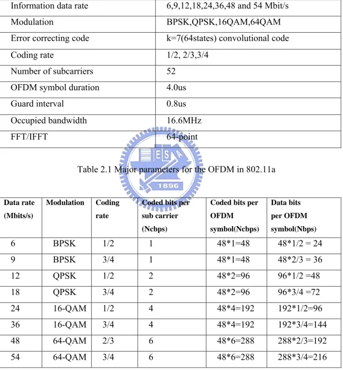
Figure 2.2 depicts the OFDM baseband system structure. All data are scrambled
with a length-127 frame-synchronous scrambler (polynomial s(x) = x7
+ x4 + 1)
before convolution encoding. Thus, continuing zeros or ones are avoided. The
convolutional encoder uses the industry standard (polynomial g0=1338, g1=1718)
which is shown in Figure 2.1. If 1/2 rate is used, the output data volume will become twice. Besides 1/2, 3/4 and 2/3 coding rates are also used with a puncturing scheme. This thesis designs and implements the Viterbi decoder for this convolutional encoder.
Data scrambler Convolution encode Inter_leaver QAM modulation
Inverse fast Fourier transform (IFFT)
RF receiver
Digital to analogy converter (DAC)
RF transmitter Cyclic extension wave shaping
Fast Fourier Transform(FFT) Channel frequency
offset and timing phase estimation Remove cyclic extension and frequency offset compensation Analogy to digital converter (ADC) Channel equalization and QAM demodulation, deinterleaver Convolution decode Data descramber Transmit data Receive data
Consider the data stream flow shown in Figure 2.2. The data sequence is first interleaved before assigned to each tone. This can combat the carrier fading channel effect. Depending on transmission rate, all data are then modulated as BPSK, QPSK, 16QAM or 64QAM symbol. Four pilot tones are added into location {-21,-7,7,21} beside 48 data location (64 tones are indexed as -32,-31,-30,…0,1,2…31), other locations will be inserted zeros. Using a 64-point inverse fast Fourier transform (IFFT), the data symbol is transformed into the time domain.
The receiver has to perform synchronization before the data can be actually demodulated. This includes the frame synchronization and the frequency offset estimation. The 64-point fast Fourier transform (FFT) block transform the data back to the frequency domain. All the process performed in the transmitter will be reversed such as symbol mapping and interleaving. The Viterbi decoder is then used to decode the convolutionally encoded data. Finally, the receiver obtains the transmit data by descrambling the Viterbi outputs.
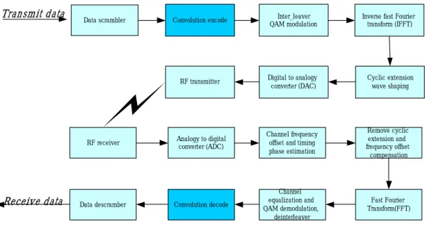
Figure 2.3 gives an example for the data flow. We assume that the transmit signal is a stream of 96-bit data. A stream of 192 bits will be obtained after the convolutional encoder. If bit 0 is fed into the encoder, we will have two output bits which are denoted as “0a_0b” in Figure 2.3. All bits will be generated by this way. All encoded
bits shall be interleaved by a block interleaver. The block size depends on the number
of coded bit per symbol (NCBPS) and NCBPS is 192 for this example. The data will be
interleaved by two-step permutation which is defined in (2.1) and (2.2), respectively. After interleaving, the resultant bits will be assigned to each subchannel, and mapped as symbols fed into the IFFT module. The receiver part will reverse operations
performed at the transmitter side. The data will first be transferred to the time domain to the frequency domain by the FFT module. Then, all symbols will be demapped as coded bits. Before convolution decoding, we have to perform deinterleaving; the operation is defined in (2.4) and (2.5), respectively. Finally, the Viterbi decoder will decode the 192-bit data into 96-bit data.
i=(NCBPS/16)(k mod 16)+floor(k/16) k =0,1…, NCBPS-1 (2.1)
j=s * floor(i/s) + (i + NCBPS-floor(16 * i/ NCBPS)) mod s i=0,1…, NCBPS-1 (2.2)
s=max(NBPSC/2,1) (2.3)
i =s * floor(j/s) + (j + floor(16 * i/ NCBPS)) mod s j=0,1…, NCBPS-1 (2.4)
Figure 2.3 Data stream from transmitter to receiver (using 16QAM modulation)
I(t)+Q(t) I(t)+Q(t) Data interleave Channel data assignment Data symbol mapping 0 1 2 3 94 0a _0b 1a _1b 2a _2b 94a _94b 95a _95b 3a _3b 95 0a_1 0b_2 1a_3 1b_4 94a_189 94b_190 95a_191 95b_192 0a_1 0b_2 1a_3 1b_4 94a_189 94b_190 95a_191 95b_192 ch1 ch2 ch48 a+jb a+jb a+jb IFFT a+jb a+jb a+jb Symbol demapping FFT xx_0 xx_1 xx_2 xx_3 xx_188 xx_189 xx_190 xx_191 ch1 ch48 ch2 0a_1 0b_2 1a_2 1b_2 94a_189 94b_190 95a_191 95b_192 0a _0b 1a _1b 2a _2b 3a _3b 94a _94b 95a _95b 0 1 2 3 94 95 Data deinterleave Viterbi decoder input Input 96-bit data Data encode: generate 192bit Output 96-bit data
2-3 Coded OFDM systems
The OFDM scheme can provide good spectral efficiency for multicarrier transmission. This is because each sub-carrier can overlap with others and
interference will not result. In conventional systems, when the transmission data rate is high, the ISI become a problem difficult to solve. Since a guard-interval is provided, it can be shown that as long as the guard interval is longer then the maximum channel delay, the OFDM system can be free of the ISI problem.
Besides, the OFDM system uses multicarriers to transmit data. For each carrier, only flat fading will result. This will facilitate the data detection in fading
environments. To avoid the deep fade in some specific carriers, the interleaving and channel coding are used [10]. This approach can make the bit error rate (BER)
performance approximately equal for all tones. The convolutional encoding (k=7) was selected by IEEE 802.11a. With the Viterbi decoding, this coding scheme can provide desired BER. The coded OFDM architecture provides a reliable solution for high data rate communication systems.
Chapter
3
The Viterbi decoder design
3-1 Viterbi algorithm
In 1967, Viterbi developed a decoding algorithm for convolutional codes, which is referred to as the Viterbi algorithm. The Viterbi decoder consists of three main building blocks: a BM computation unit (BMU), the add-compare select unit (ACSU), and the survivor memory unit (SMU). Both the BMU and the ACSU perform
arithmetic operations and the results are stored in the SMU. The most likely transmit sequence is found by the trace back operation in the SMU. The detailed operation will be addressed in the following.
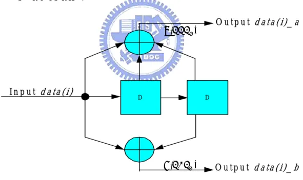
In order to establish the Viterbi principle, it is convenient to start with the convolution encoding first.
D D O u t p u t d a t a ( i ) _ a O u t p u t d a t a ( i ) _ b I n p u t d a t a ( i ) ) 111 ( 7 2 ) 101 ( 5 2
Figure 3.1 Convolutional encoder (rate ½ k=3 m=2)
Figure 3.1 shows a k=3, (7,5) convolutional encoder. The numbers 7 and 5 represent the code generator polynomials. They can be read in binary format as 1112
1012; each binary number indicate that if the shift register output is connected to the
state. Table 3.1 shows the state transaction. The encoder behavior then follows that described in the table. For example, if the current state is “00” and input data is “1”, the encoder output must be “11” and the state transits to “10” state.
Current input=0 input =1 I
State next state output symbols next state output symbols
00 00 00 10 11
01 00 11 10 00
10 01 10 11 01
11 01 01 11 10 Table 3.1 The state translation table
We now use a simple example to describe the Viterbi algorithm. Let the transmit data stream be (0101-1101). Using the encoder in Figure 3.1, the data stream after encoding is then (00111000-01100100). Also, let the received sequence be
(00111100-01100100). Note that there is one bit erroneously detected at receiver (the
six-th bit),
In the receiver, the Viterbi algorithm uses a trellis diagram to trace the data
transition and select a sequence with maximum likelihood. We depict the operations in Figure 3.2. For example, from time t0 to t1, the received pair symbol is ”00”. We can then calculate the BM for input bit “0” and “1”. We denote these metrics as BM1 and BM2. It is simple to have that BM1=0 BM2=2 (the Hamming distance from the received pair symbol to the encoder output). For time t1 to t2, we then have four BMs to compute. Using the similar notations, we have BM3=2, BM4=0, BM5=1, and BM6=1. We now can calculate the PM, which is an accumulation of BMs, from t0 to t2. Denote the PM from t0 to the state “ij” at t2 as PMij_2. We then have four PMs to compute. We can find that PM00_2, obtained from BM1+BM3, is 2. Similarly, we can obtain PM01_2=3, PM10_2=0, and PM11_2=3. Figure 3-2 (b) and Figure 3-2 (c) show the trellis transition from t2 to t3 and t3 to t4, respectively. As shown are PMs calculated for all paths at each time unit. Table 3.2 shows the PM values at each time
states and find the state transition sequence. Table 3.3 gives “surviving predecessor states “. Figure 3.3 displays the trellis trace back path. Along with the trace back, we can decode the data according to the state transition table (Table 3.1). We finally obtain the decoded data as “0101- 1101” which is identical to the transmit ones. time t0 t1 t2 state00 state01 state10 state11 Encoder Out 00 11 Receiver 00 11
Figure 3.2 (a) Viterbi decoder trellis diagram (1)
time t0 t1 t2 t3 state00 state01 state10 state11 Encoder Out 00 11 10 Receiver 00 11 11
Figure 3.2 (b) Viterbi decoder trellis diagram (2)
BM3=2 00 00 11 11 BM1=0 BM2=2 BM4=0 BM5=1 BM6=1 01 PM00_2=BM1+BM3=2 PM01_2=BM2+BM5=3 PM10_2=BM1+BM4=0 PM11_2=BM2+BM6=3 BM8=0 BM9=1 BM10=1 BM11=1 BM12=1 BM13=1 BM14=1 01 10 00 10 11 00 BM7=1 01 10 PM00_3=PM00_2+BM7=3 or PM00_3=PM01_2+BM9=4 PM01_3=PM10_2+BM11=1 or PM01_3=PM11_2+BM13=4 PM10_3=PM00_2+BM10=4 or PM10_3=PM01_2+BM8=2 PM11_3=PM10_2+BM12=1 or PM11_3=PM11_2+BM14=4 10
time t0 t1 t2 t3 t4 state00 state01 state10 state11 Encoder out 00 11 10 00 Receive 00 11 11 00
Figure 3.2 (c) Viterbi decoder trellis diagram (3)
time t0 t1 t2 t3 t4 t5 t6 t7 t8 state00 state01 state10 state11 Encoder in 0 1 0 1 1 1 0 1 Encoder out 00 11 10 00 01 10 01 00 Receiver 00 11 11 00 01 10 01 00
Figure 3.3 Viterbi decoder trace back path
00 BM15=0 BM22=1 BM21=1 BM17=2 BM20=1 BM18=0 BM19=1 00 11 10 10 01 01 BM16=2 PM00_4=PM00_3+BM15=3 or PM00_4=PM01_3+BM17=3 PM01_4=PM10_3+BM19=3 or PM01_4=PM11_3+BM21=2 PM10_4=PM00_3+BM16=5 or PM10_4=PM01_3+BM18=1 PM11_4=PM10_3+BM20=3 or PM11_4=PM11_3+BM22=2 11
t0 t1 t2 t3 t4 t5 t6 t7 t8 state00 0 2 3 3 3 3 4 3 state01 3 1 2 2 3 1 4 state10 2 0 2 1 3 3 4 1 state11 3 1 2 1 1 3 4 t0 t1 t2 t3 t4 t5 t6 t7 t8 state00 0 0 0 1 0 1 1 0 1 state01 0 0 2 2 3 3 2 3 3 state10 0 0 0 0 1 1 1 0 1 state11 0 0 2 2 3 2 3 2 3
Table 3.3 Surviving predecessor states from t0 to t8 Table 3.2 Path metrics from t0 to t8
3-2 Hard decision and soft decision
The decoder described in the previous section is a hard-decision decoder which uses a Hamming distance metric in the BM calculation. As mentioned, the
computational complexity is low, but its BER is higher.
The soft-decision Viterbi decoder replaces the Hamming distance metric with the Euclidean distance metric. It can explore more useful information and enhance the Viterbi decoder performance.
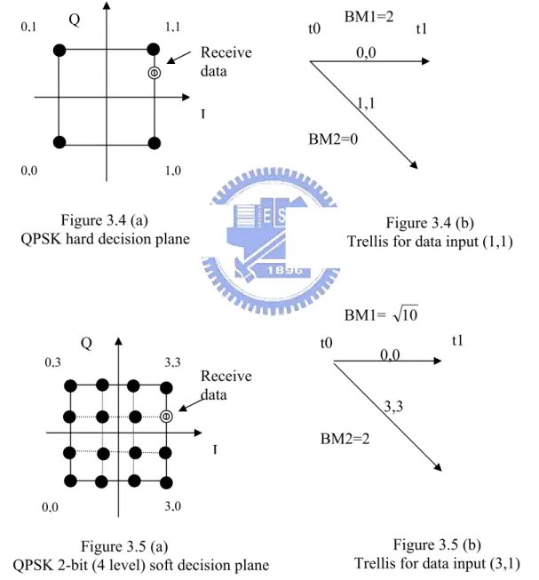
Figure 3.4 (a) shows the decision plane for a QPSK modulation. Any received
1,1 1,0 0,1 0,0 3,3 3,0 t1 t0 0,0 1,1 BM1=2 0,3 0,0 t1 t0 0,0 3,3 BM2=2 BM1= 10 Figure 3.5 (a)
QPSK 2-bit (4 level) soft decision plane
Figure 3.5 (b) Trellis for data input (3,1) Figure 3.4 (a)
QPSK hard decision plane Trellis for data input (1,1)Figure 3.4 (b)
Receive data Receive data I Q I Q BM2=0
One QPSK symbol carries two bits data in I and Q branch. In the hard-decision
scheme, the received symbol is equivalently be quantized to one bit in I and Q branch. In other words, one QPSK symbol will be represented as two bits in the hard-decision scheme. Figure 3.4 (b) shows that the hard-decision scheme uses the Hamming distance to calculate BMs as those in (3.1) and (3.2).
Figure 3.5 (a) shows a 2-bit soft-decision Viterbi scheme. The received symbol can then be quantized to one of 16 possible symbols. This is because two bits have been used for I and Q branch. In Figure 3.5 (a), the received symbol is quantized as symbol (3,1) and this serves as the Viterbi decoder input. Figure 3.5 (b) shows the soft decision trellis diagram. Using the Euclidean distance metric, we find that the BMs are those shown in (3.3) and (3.4). Since the Viterbi decoder is a maximum likelihood decoder, the more quantization bits, the better performance we will obtain.
For the WLAN application, it has been shown that a three-bit quantization results in a performance improvement about 2 dB then a two-bit quantization [17]. Quantization with more then 6 bits can yield very little performance improvement.
BM1=XOR {(0,0),(1,1)} =2 (3.1)
BM2=XOR{(0,0),(0,0)} =0 (3.2)
BM1= (0−3)2+(0−1)2 = 10 (3.3)
3-3 Hard decision weighting
From the previous section, we know that the hard-decision Viterbi scheme is simple but may not have satisfactory performance. In this section, we propose a new algorithm, which is as simple as the hard-decision decoder but enjoys higher
performance. We call this algorithm as a hard-decision weighting decoder.
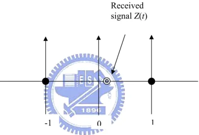
We use a simple example to describe our idea. Figure 3.6 shows the decision plane for a BPSK modulation. Note that due to noise, the received symbol r can be located at anywhere in the x-axis. For hard-decision, if r > 0, the decision as 1, otherwise it is -1. The decision region for 1 is (0,∞) and the decision region for –1 is then (-∞,0)
Take two received signals r = 0.1 and r = 1 as examples. Both decision are “1” by the hard-decision principle. However, it is simple to see that the confidence for the decision is different for these two signals. Of course, soft-decision can solve the problem easily, but it requires higher computational complexity. It is our objective to solve this problem using a simple way.
The basic idea for “hard decision weighting” scheme is simple. For each decision region, we further partition it into two regions; the first one is considered reliable and the second one is not reliable. In the BM calculation, we then increase the weight if
-1 0 1
Figure 3.6 BPSK decision plane Received signal Z(t)
n is an integer). Consider a special BPSK scenario that the transmit symbol is either
a1 or a2. The received signal is then r = a+n0 where a can be a1 or a2 and n0 is additive
white Gaussian noise with mean zero and varianceσ2. Figure 3.7 illustrates the conditional probability density function (PDF) for the binary noise-perturbed received symbol. The ML decision gives
2 where if , 1 if , 1 ˆ 2 1 a a r r a + = < − ≥ = γ γ γ
The probability of error shown in the shaded are in Figure 3.7 is then
where Q(.) is the complementary error function.
p robab ili ty ∞
2
/
)
(
a
1+
a
2 2a
1a
bP
Figure 3.7 Received symbol distribution (1) We now want to find the threshold, γ1, that determines weighting regions.
Without loss of generality, we let a1= -1, a2=1, and σ=1. Also, let the transmit symbol
− = − ∫∞ = − − ∫∞ = σ γ σ π σ γ σ π 2 2 exp 2 1 ( 2 1 exp 2 1 2 1 2 2 2 a a Q du u dz a z Pb (3.5) (3.6)
be from a2. Figure 3.8 shows the received symbol distribution. In the figure, note that
1
γ =1-
s
1. For our algorithm, we add weighting on the BM calculation when thereceive signal is in the area “A” (the interval between –s1 and a2). First, we define a
cost function (3.7) that measures the probability of correct weighting and incorrect weighting. (A) (B) (C) (D) (E) (F) 1 2=− a a1=1 ) 0 ( Q ) 1 ( Q ) 1 ( ) ( 1 Q Q γ − ) ( ) 0 ( Qγ1 Q − ) 2 ( ) 1 ( − Q −γ1 Q ) 0 ( Q ) 1 ( Q ) 2 ( −γ1 Q 1 s − 1 1 1= −s γ 0 = s Figure 3.8 Received symbol distribution (2)
)] 1 ( ) ( )[ 2 ( )] 2 ( ) 1 ( )][ ( ) 0 ( [ ) ( 1 Q Q 1 Q Q 1 Q 1 Q 1 Q J γ = − γ − −γ − −γ γ − (3.7)
Note that Q(0)-Q(γ1) indicates the probability that the transmit symbol is from
a2 and the receive signal is in the area “A”. In other words, the hard-decision is
correct and the weighing should be carried out. The term Q(1)-Q(2-γ1) indicates the
probability that the transmit symbol is from a1 and the receive signal in the area “E”.
probability of correct weighting for symbols from a1 and correct “not weighting” for
symbols from a2. Now, the term Q(2-γ1)gives the probability that the transmit symbol
is from a1 and the receive signal is in the area “D”. In this case, it should no be
weighting; however, it is weighted. Thus, the weighting is incorrect. Finally, the term
Q(γ1)-Q(1) gives the probability that the transmit symbol is from a2 and the receive
signal is in the area “B”. It should be weighted; it is not actually. This is incorrect either. Thus, the second term on the left hand side of (3.8), which is the product of two probabilities, indicates the joint probability of incorrect weighting for symbols
from a2 and incorrect “no weighting” for symbols from a1. The cost function then
corresponds to the relative probability of correct weighting decision. We then
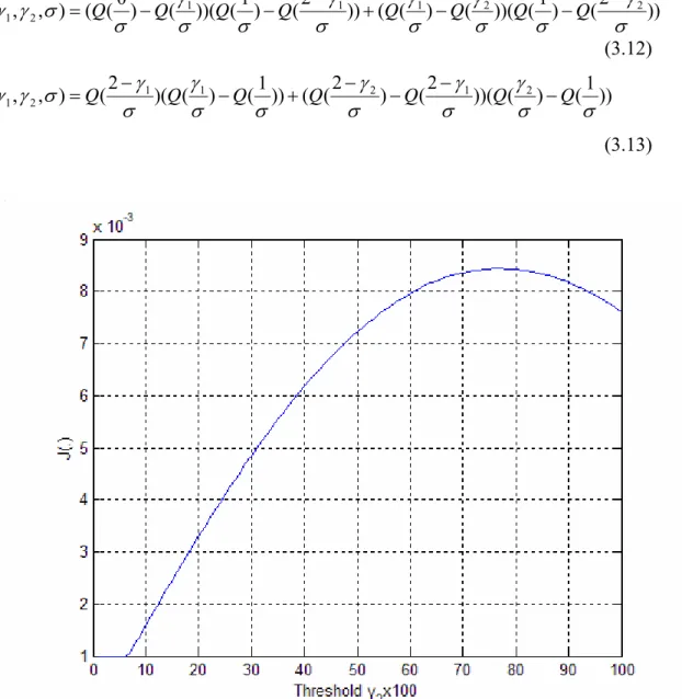
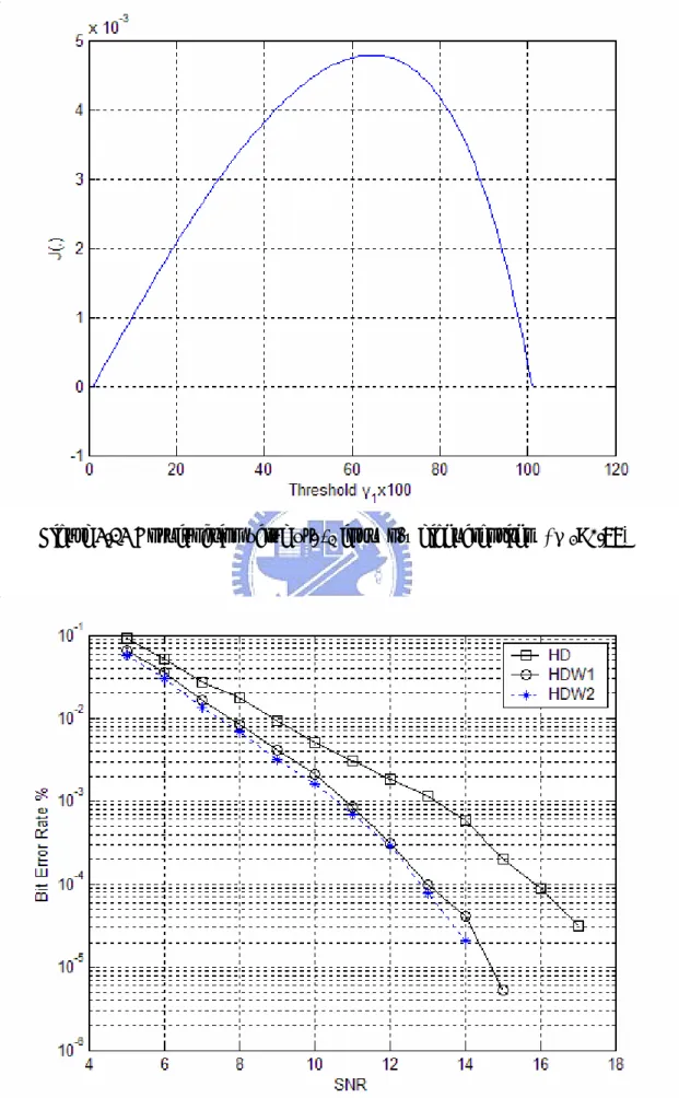
minimize the cost function in (3.8) and obtain the optimal threshold. Figure 3.9 shows the cost function vs. the threshold. We can see that the optimal threshold is around 0.6.
r
Figure 3.9 The cost function vs. threshold
The SNR used is7 dB here. We have found that the optimal threshold is between 0.6
and 0.75 when the SNR varies from 0 to 20 dB. The optimal threshold is not sensitive to the SNR. We can generalize (3.7) to have the optimization criterion for the general
noise case scenarios as )] 1 ( ) ( )[ 2 ( )] 2 ( ) 1 ( )][ ( ) 0 ( [ ) ( 1 1 1 1 1 σ σ γ σ γ σ γ σ σ γ σ γ Q Q Q Q Q Q Q J = − − − − − − (3.8)
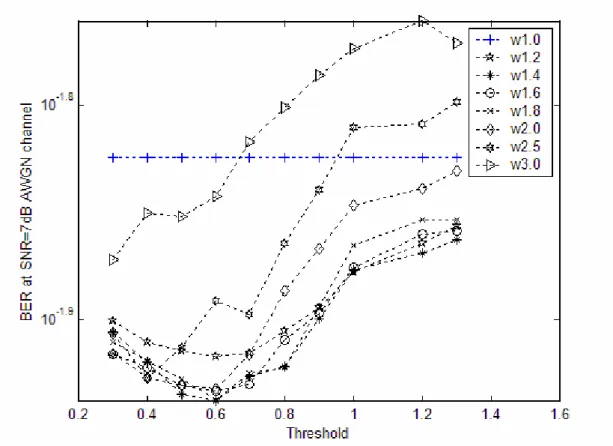
After finding optimal thresholds, we then have to determine how much weight we should give. Since this is something to do with the Viterbi algorithm, it is difficult to find a criterion to optimize. We then use simulations to find the optimal one. Figure 3.10 shows the simulation results. In the figure, “w1.0” indicates the results without weighting, “w1.2” indicates the results with weighting (weight is 1.2), and so on. From the figure, we found that if the weight value is between 1.1 and 2, the Viterbi performance is similar. Also note that the optimal threshold is around 0.6. The SNR used here is 7 dB. Other cases will give similar results. We then use 0.625 as the threshold and 2 as the weight for simplicity.
Figure 3.10 BER vs. threshold and weight
find optimal thresholds, we can formulate a criterion similar that in (3.8). The resultant cost function is shown in (3.9).
) , ( ) , ( ) , (γ1 γ2 P1 γ1 γ2 P2 γ1 γ2 J = − (3.9) where )) 2 ( ) 1 ( ))( ( ) ( ( )) 2 ( ) 1 ( ))( ( ) 0 ( ( ) , ( 1 2 1 1 1 2 2 1 γ γ = Q −Q γ Q −Q −γ + Q γ −Q γ Q −Q −γ P (3.10) )) 1 ( ) ( ))( 2 ( ) 2 ( ( )) 1 ( ) ( )( 2 ( ) , ( 1 2 1 1 2 1 2 2 Q Q Q Q Q Q Q P γ γ = −γ γ − + −γ − −γ γ − (3.11) (A) (B) (C) (D) (E) (F) (G) (H) ) 0 ( Q ) (γ1 Q ) 1 ( Q ) 1 ( Q Q(0) 0 = s 1 s − −s2 ) 1 ( ) ( 2 Q Qγ − ) ( ) 0 ( Q γ1 Q − ) ( ) (γ1 Q γ2 Q − ) 1 ( ) ( 1 Q Qγ − ) 2 ( ) 1 ( − Q −γ1 Q ) 2 ( ) 1 ( − Q −γ2 Q ) 2 ( ) 2 ( −γ2 −Q −γ1 Q ) 2 ( −γ1 Q 1 1=1 s− γ 2 2=1 s− γ 1 2=− a a2=1
Figure 3.11 Received symbol distribution (3)
thresholds are found to be γ1=0.77 and γ2=0.5. The optimal weights are found to be
around 2 and 1.5. We can generalize (3.10) and (3.11) to obtain the optimization criterion for the general noise case as
)) 2 ( ) 1 ( ))( ( ) ( ( )) 2 ( ) 1 ( ))( ( ) 0 ( ( ) , , ( 1 1 1 2 2 2 1 1 σ γ σ σ γ σ γ σ γ σ σ γ σ σ γ γ = Q −Q Q −Q − + Q −Q Q −Q − P (3.12) )) 1 ( ) ( ))( 2 ( ) 2 ( ( )) 1 ( ) ( )( 2 ( ) , , ( 1 1 2 1 2 2 1 1 σ σ γ σ γ σ γ σ σ γ σ γ σ γ γ Q Q Q Q Q Q Q P = − − + − − − − (3.13)
Figure 3.13 Cost function value vs. γ1 for two-weight algorithm (γ2=0.77)
Figure 3.14 illustrates the BER performance for various Viterbi algorithms (in AWGN environment). In the figure, HD denotes the conventional hard-decision decoding, HDW1 denotes the proposed one-weight algorithm, and HDW2 denotes the proposed two-weight algorithm. As we can see, the proposed hard-decision weighting
algorithm outperforms the hard-decision algorithm by 2dB at BER=10-3. The
two-weight algorithm only performs slightly better than the one-two-weight algorithm. For this reason, we then use the one-weight algorithm in our implementation. As we
mentioned, the hard-decision weighting algorithm only needs XOR logic operations to compute BMs and its computational complexity is lower.
3-4 Viterbi decoder with receiver diversity
In the WLAN environment, the multipath channel effect may affect the receiver performance significantly. It is known that the diversity technique can effectively solve the problem. Space diversity is a popular and effective diversity technique and its can be easily applied in WLAN systems. In this approach, an antenna array is used in the receiver. There can be different various implementation
architectures for the antenna diversity. The first one shown in Figure 3.15is called
the antenna selection. In this architecture, we need only one RF module although L antennas are used. This architecture only selects the antenna with the strongest output for processing. Baseband processing is not affected at all and its
implementation cost is lowest. However, its performance enhancement capability is
limited. For other structures we require L RF modules in general. Figure 3.16shows
the architecture. Outputs from RF modules are first down converted, sampled, and transformed using FFT. Various diversity combing methods can then be applied. We only discuss the optimal one, which is the maximum ratio combing (MRC).
R F C IR C U IT D S P MU X C o m p a ra to r A n te n n a 1 A n te n n a 2 A n te n n a N
C o m b in in g R F C IR C U IT R F C IR C U IT R F C IR C U IT D SP FFT FFT FFT
Simulations indicate that this scheme can enhance10dB performance with two receive antenna in an exponential decay AWGN channel. The performance enhancement is significant. Let the received signal for the ith tone signal of a nth
symbol at the jth antenna be Xij(n), and the corresponding transmit signal, channel,
and noise beSij(n), )H (n j i , and V (n) j i , respectively. Then, ) ( ) ( ) ( ) (n H n S n V n X ij j i j i j i = + (3.14)
The MRC output signal, denoted by Sˆ ni ( ), is then
∑
∑
= = ∗ = L j j i L j j i j i i n H n X n H n S 1 2 1 | ) ( | ) ( )] ( [ ) ( ˆ (3.15)Note that the conventional approach uses diversity combing first and then pass the result to the Viterbi decoder. We call this observation MRC (OMRC). We propose
antenna is the kth be zijk(n). We then have a new BM as
∑
= = L k k ij ij z n z 1 ) ( (3.16)As we can see, this BM takes all the observations from all antennas into account. Since the channel effect is taken into account, it will give the MRC-like results for the Viterbi algorithm. We call this a Viterbi MRC (VMRC) algorithm.
Simulation results for an exponential decay AWGN channel are shown in Figure 3.17. Here, two antennas are used for the diversity approach. From the figure,
we can see that at BER=10−4, the OMRC and the VMRC outperform the decoder
without diversity (NORMAL) by 9dB and 11dB, respectively. Apparently, the VMRC outperforms the OMRC by 2 dB. The gain is significant.
We then add more antennas and carry out more simulations Figure 3.17 shows the results. In the figure, the solid line with symbol “+” indicates the result with the
decoder without diversity. Solid lines with symbols “o”, “ * ”, and “+” indicate the performance of the OMRC with two, three, and four antennas, respectively (denoted as OMRC2, OMRC3, and OMRC4). Dashed lines with symbols “o”, “ * ”, and “+” indicate the performance of the VMRC with two, three, and four antennas,
respectively (denoted as VMRC2, VMRC3, and MRC4). From these results, we can clearly see that the VMRC is always better than the OMRC. When the number of antenna is larger, the performance gap becomes larger also.
Figure 3.18 Comparison between NORMAL, OMRC2, OMRC3, OMRC4, VMRC2, VMRC3 and VMRC4
3-6 Memory management and adaptive tracing back
The REM (register exchange method) is simple, but it is not efficient for the WLAN system since it requires high power consumption and large chip area. Thus, we employ the TBM as our implementation scheme. This section addresses the memory management scheme for the TBM.
There are several trace back algorithms known as, the K-pointer even algorithm, the
K-pointer odd algorithm [18], the one-pointer algorithm, and the hybrid algorithm. In
one- pointer trace back architecture [6], it only uses a single read pointer and needs approximately half as much memory as other approaches. The disadvantage of the one-pointer algorithm is that we need to provide separate column counters for the write and read operations individually. Another disadvantage is that the trace back operation clock must be three times as fast as the writing operation clock if the read region is three times as large as the write region. Since in the WLAN application, the clock rate is not particularly high, we then adopt this memory management method in our implementation.
Figure 3.19 shows the one-pointer algorithm operation. Here, “TB” denotes the track back read. This operation is to find out the previous state according the data stored in the memory. There are two banks memory for trace back and this implies that this Viterbi decoder trace back with depth 2T. The notation “DC” means the data decode read. The first decode read (starting state) in a memory bank is determined by the previously two track back bank result. The decoder reads the newer data, decode them, and send them to the LIFO (last in first out) register performing the bit-order reverse. The operation “WR” means decoder new data write. Decisions, indicating the previous surviving state, are made by the ACS and written into locations representing corresponding states.
We now explain the operations outlined in Figure 3.19. We assume that the time interval between t0 and t1 is a unit time, so is that between t1 and t2 (and so on). During the T0 interval (between t0- t1), one write pointer points out the write location
and ACS out data is written into bank0 memory.In the same time, one read pointer
starts tracking back and reading data from bank3 memory. The read pointer is
operated as three times faster as the write pointer. Thus, the write operation only fills 1/3 bank0 memory when the “TB” has finished bank3 memory track back. Then, at
time t2, the trace back operation has terminated at the end of bank2 memory, the write operation fills 2/3 bank0 memory. Finally, the decoder read bank1 memory and finishes the decoding operation at t3 and the write operation fills bank0 memory at the same time. During the T3 (t3-t4) time period, we then shift the read/write pointer as that shown in Figure 3.19 and repeat the operations all over again. We can obtain the data out from the decoder continually.
Figure 3.19 displays the memory organization for storing the survivor path. Here, the memory depth for each bank is Γ. In order to find the optimal decode starting state, we have to trace back two memory banks before decode. In other words, the trace back length is 2Γ. One data output from the decoder must have four memory accesses; the first is “WR” data write. When the memory bank is full (3/3 WR), we will start trace back for the next time unit. After two times trace back, we then have the decode (DC) operation. Since the trace back unit contributes almost half of power dissipation (the trace back length is 2Γ). Howe to reduce the memory access
frequency during the trace back is then the main concern.
Figure 3.19 One-pointer trace back method
Figure 3.20 also shows the Viterbi decoder memory trace back paths. As we can see if the trace back length is long enough, all the trace back paths will merge at some block. Figure 3.21 illustrates the trace back path within two memory banks; the solid line indicates one trace back path and dash lines indicate other trace back paths. It is desirable that all paths merge before the decode block. It means that trace back from
DC TB
BANK0 BANK1 BANK2 BANK3
DC DC TB TB TB TB TB 1/3wr TB TB Γ T0(t0-t1) T1(t1-t2) T2(t2-t3) TB T3(t3-t4) TIME 1/3wr 2/3wr 3/3wr
Before the trace back, we can guess a terminating state having a minimum PM in the previous memory block. In the writing operation, we can record all possible states (at each time instant) that can reach the terminating state. Then, if the trace back starting state is in these states, we can immediately know that the track back will end with the terminating state we guessed; we call this case as a “trace forward hit”. Figure 3.21 shows an example. In the figure, the state (s35) with the minimum PM in the previous block is written at t=0. When t=1, we found that only one survivor path (s17) is from s35 and we record this state (s17) by writing a “1” in a 64x1 register array. This means that if trace back starts from state17 (s17), it will go through the state (s35). When t=2, there are two survivor paths coming from the state (s17). We record these two states (s8) (s40) by writing two “1”s in the register array (note that the array is reset before writing). These two “1”s indicate that if trace back starts from state8 (s8) or state40 (s40), it will go through the state (s35) in the end. When t=3, there are three survivor paths coming from the previous two states. We then write three “1”s in the 64x1 register array. As the writing process proceeds, the values in the register array are updated. Finally, at t=n, the register array remains four “1”s indicating states s2, s8, s32, and s63. The four states imply that if trace back starts from state2 (s2), state8 (s8), state32 (s32), or state63 (s63), it will terminate at s35. Thus, we can skip the trace back operation in the memory block. This will reduce the memory access frequency. Figure 3.22 illustrates this skip scheme. When bank0 is decoded, we write data to bnak3 and record the trace forward states. After the decoding in bank0 is finished, we write data to bnak1 and starts trace back from bank3. If the state with the minimum PM is in the trace forward states, the track back operation in bank3 will be skipped (see T1). If once again, the trace forward is hit in bank0. At T3, we can skip the trace back in bank0 and bank3.
DECODE
BLOCK MERGE BLOCK
TB TB
DC
Unfortunately, the “trace forward” is not always hit. Figure 3.23 shows the hit rate with different SNR in AWGN channel. It is obviously that a higher hit rate appears in a higher SNR environment. The percentage that the memory access activity can be reduced is shown in Figure 3.24.
t=0 t=1 t=2 t=n-1 t=n
time Previous block
minimum path metric state
current block minimum path metric state
(s35) (s32 ) (s63) (s8) (s2 ) (s8) (s17) (s40) (s36) (s2 0) (s52 ) t=3 WR TB1 TB2 DC TB1 TB2 DC WR WR DC TB1 TB2
Bank0 Bank1 Bank2 Bank3
Figure 3.23 Trace forward hit rate with different SNR
As we can see, when the SNR is 12 dB, the “look forward” scheme can save only 45% memory access activity. Note that the hitting rate is over 90%. This is because “WR” and “DC” are still needed. To further reduce the memory access frequency, we need to merge these two operations
The advance minimum-transition trace back (AMTTB) scheme in[3] is the
algorithm can further reduce the memory access activity. Figure 3.25shows the
operation. Here, we assume that the trace back depth is 32 and the size for each memory bank is 64x32. We need one extra predict buffer 1x32 for storing the data for the most likely path. In the write operation we record the most likely trace back path in the predict buffer. In the trace back stage, read data from the memory bank, find the previous state, and compare the read data with the predict data. If these data are different, modify the data in the predict buffer. Otherwise, the trace back operation is replaced by reading the predict buffer only. This is because the trace back has merged at this point and we do not have to read the memory bank. By using so, we can substantially reduce the memory access frequency in the trace back and decode stages. How munch the memory access times can we save? It depends on the merge point. Table 3.4 shows some simulation results. It indicates that in most cases, the prediction hits at first trace back stage. Almost all cases will be hit (merged) before the decode stage. This scheme can reduce the memory access frequency significantly. However, we have to add an extra trace back circuit.
Figure 3.25 Minimum-transition trace back operation scheme WR DC TB1 Compare and modify buffer Predict buffer 1*32 TB2 Compare and modify buffer Predict buffer 1*32 Predict buffer 1*32 Predict buffer 1*32
Prediction Hit distribution
Table 3.4 Minimum-transition trace back hit rate distribution SNR 18 19 20 21
Hit 1stage 79.9286 84.0000 89.5000 91.0714 Hit 2stage 97.7857 98.2143 99.2857 99.4286
Chapter 4
Low power Viterbi decoder implementation
4-1 Design and implementation flow
Figure 4.1 shows our design and implementation flow. The first step is to study algorithms and choose the best solution for our requirement. Then, we carried out simulations to realize its behavior and evaluate its performance. In this stage, we often use a high level language such as C language or MATLAB. Algorithm study and simulation must be repeated until it passes the performance requirement. The next step is to use VHDL for low-level modeling. Then, we perform RTL (Function) simulations to make sure the model work properly. Using the standard cell library, we then synthesize our design to the gate level. Finally, the gate level simulations were conducted to verify the circuit timing and functionality. Power analysis is import since the low power and low complexity is our design target. We use Prime Power to analyze the average and peak power consume for our design. We are interested to know how much power reduced by the various designs. To evaluate the chip area consumed, we can use a FPGA (field programmable gate array) for the circuit implementation. The routing and simulation are simple in the FPGA implementation flow. Algorithm study Algorithm simulation RTL coding Function simulation Synthesize and gate level simulation Power analysis
4-2 Implementation of Viterbi algorithm
Figure 4.2 illustrates a 802.11a channel decoder architecture. The receive symbol is first de-mapped and de-interleaved and then forwarded to the Viterbi decoder. The decoded bits are stored in the LIFO data buffer. After the LIFO, data are transferred to the media access control (MAC) module. It is the Viterbi decoder module that we implemented.
Figure 4.3 shows our design block diagram for 802.11a Viterbi decoder. There are four memory banks and each one with size of 64x32. That means we have 64 states and the track back depth is 32. Besides the main memory, we also have to implement the prediction buffer for each memory bank. The predicted trace back can reduce the memory access frequency as described before. The predict buffer has the size of 32x1.
Memory banks and predict buffers are controlled by the memory controller and the buffer controller individually. The decoder controller, which includes the decoder main state machine, receives the input frame enable signal and outputs the decoded results. The BMU is responsible for BM calculation and the BM weighting. The result from the BMU is then transferred to the ACSU for each cycle. The ACSU feeds all the memory banks with survivor path data. This module also needs to perform the PM calculation and the PM comparison. Since these operations cannot be pipelined, the timing bottleneck for the decoder is in this unit. We will further discuss the topic in Section 4-4. In our design, the memory bank uses the Verilog model made by
Symbol De-mapping
Data buffer
de-interleave Viterbi Decoder Data buffer MAC
“Artisan“. The memory compiler can be used to obtain the corrsponding VHDL design. When transferring our design to FPGA, the compiler will be replaced by the Xilinx memory compiler.
Predict buffer (64bit)
RegFile_A 64X32
Predict buffer (64bit)
RegFile_A 64X32
Predict buffer (64bit)
RegFile_A 64X32
Predict buffer (64bit)
RegFile_A 64X32
Buffer controller
Decoder controler
Memory controller
Branch Metric Unit (BMU)
Add Comparator Selector Unit
(ACSU)
Decoder output data
Frame enable
Decoder input data
64 bit write data
4-3 Over flow consideration
Figure 4.4 illustrates the trellis diagram for the 802.11a Viterbi decoder. Here, s00 indicates state-00 and it will transfer to s00 (state-00) or s32 (state-32). All other state transactions can be obtained using this figure. Using this figure, we construct the
ACSU module. Figure 4.4 shows the ACSU structure. Since thevalue in the PM is
accumulated, it should be normalized (after all comparators) to avoid PM over flow. The modulo arithmetic approach [9] [20] can then be used here.
S 0 0 S 0 1 S 0 2 S 0 3 S 0 4 S 0 5 S 0 6 S 0 7 S 0 8 S 0 9 S 1 0 S 1 1 S 1 2 S 1 3 S 1 4 S 1 5 S 1 6 S 1 7 S 1 8 S 1 9 S 2 0 S 2 1 S 2 2 S 2 3 S 2 4 S 2 5 S 2 6 S 2 7 S 2 8 S 2 9 S 3 0 S 3 1 S 3 2 S 3 3 S 3 4 S 3 5 S 3 6 S 3 7 S 3 8 S 3 9 S 4 0 S 4 1 S 4 2 S 4 3 S 4 4 S 4 5 S 4 6 S 4 7 S 4 8 S 4 9 S 5 0 S 5 1 S 5 2 S 5 3 S 5 4 S 5 5 S 5 6 S 5 7 S 5 8 S 5 9 S 6 0 S 6 1 S 6 2 S 6 3 S 0 0 S 0 1 S 0 2 S 0 3 S 0 4 S 0 5 S 0 6 S 0 7 S 0 8 S 0 9 S 1 0 S 1 1 S 1 2 S 1 3 S 1 4 S 1 5 S 1 6 S 1 7 S 1 8 S 1 9 S 2 0 S 2 1 S 2 2 S 2 3 S 2 4 S 2 5 S 2 6 S 2 7 S 2 8 S 2 9 S 3 0 S 3 1 S 3 2 S 3 3 S 3 4 S 3 5 S 3 6 S 3 7 S 3 8 S 3 9 S 4 0 S 4 1 S 4 2 S 4 3 S 4 4 S 4 5 S 4 6 S 4 7 S 4 8 S 4 9 S 5 0 S 5 1 S 5 2 S 5 3 S 5 4 S 5 5 S 5 6 S 5 7 S 5 8 S 5 9 S 6 0 S 6 1 S 6 2 S 6 3 S 0 0 S 0 1 S 0 2 S 0 3 S 0 4 S 0 5 S 0 6 S 0 7 S 0 8 S 0 9 S 1 0 S 1 1 S 1 2 S 1 3 S 1 4 S 1 5 S 1 6 S 1 7 S 1 8 S 1 9 S 2 0 S 2 1 S 2 2 S 2 3 S 2 4 S 2 5 S 2 6 S 2 7 S 2 8 S 2 9 S 3 0 S 3 1 S 3 2 S 3 3 S 3 4 S 3 5 S 3 6 S 3 7 S 3 8 S 3 9 S 4 0 S 4 1 S 4 2 S 4 3 S 4 4 S 4 5 S 4 6 S 4 7 S 4 8 S 4 9 S 5 0 S 5 1 S 5 2 S 5 3 S 5 4 S 5 5 S 5 6 S 5 7 S 5 8 S 5 9 S 6 0 S 6 1 S 6 2 S 6 3
In Figure 4.5, the “adder” block implements the PM computing in (4.11) while the comparator implements (4.12). After the minimum PM is found, one bit survivor path indicator is written to the memory bank. The new PM will be latched at the PM register (denoted as “PM_reg”) for the next state computing. The ACSU conducts the same operations cycle by cycle.
PM(A)_next state = PM(A)_current state +BM(A)_next state (4.1)
PM= min {(PM(A)_c + BM(A)_n), (PM(B)_c + BM(B)_c) } (4.2)
ad d er c o m p arato r n o rm a lizatio n P M _ reg 0
W r _ d a ta 0 ( o n e b it s u r v i v o r p a t h in d i c a to r w r i te to m e m o r y ) B M ( s0 0) _ n
P M ( s0 0) _ c
ad d e r c o m p arato r n o rm alizatio n P M _ reg 0
B M ( s0 1) _ n
P M ( s0 1) _ c
W r _ d a ta 1
ad d e r c o m p arato r n o rm alizatio n P M _ reg 0
B M ( s3 1) _ n
P M ( s3 1) _ c
a d d e r co m p arato r n o rm alizatio n P M _ reg 0
B M ( s3 2) _ n
P M ( s3 2) _ c
w r _ d a ta 3 2
ad d er co m p arato r n o rm aliza tio n P M _ re g 0
B M ( s6 3) _ n
w r _ d a ta 6 3 P M ( s6 3) _ c
w r _ d a ta 3 1
Figure 4.5 Structure of adder comparator selective unit (ACSU)
There are many solutions to solve the PM over flow [20] problem. These includes the reset, the difference metric ACS, the variable shift, the fixed shift, and the modulo normalization algorithm. Among them, the modulo
normalization with a modified comparator is well suited to VLSI implementation.
The key idea for modulo normalization is that the difference between two
survivors path is bounded [19]. Denote the bounded value as c. Let mj be a
variation of θ1and θ2. If |m1-m2|< c/2, then m1-m2= m1-m2. When σ < 180°, then
m1<m2. Note that sincem1 and m2are signed numbers, we have to use a
subtractor to perform comparison.
We can use a modified comparator to replace the subtractor and reduce the
computational complexity. Let m1=( m1,p,…, m1,0) and m2=( m2,p,…, m2,0)
be the two’s-complement representations for m1 and m2. Equation (4.6) show
the operation in which “^” indicates exclusive-or operation , y(.,.) unsigned comparison, and Z(.,.) the comparison result.
2 ) mod( ) 2 (m c c c mj ≡ j + − (4.3) 1 m = j p j j m 2 0 , 1
∑
= m =2 j p j j m 2 0 , 2∑
= (4.4) P1= j p j j m 2 1 0 , 1∑
− = P2= j p j j m 2 1 0 , 2∑
− = (4.5) Z(m1,m2)=m1,p^m2,p^ y(P1, P2) (4.6) . 2 c −This approach can speed up the normalization operation since m1^m2 and
y(P1,P2) can be performed in parallel and subtraction operation is not required.
0
Figure 4.6 Modulo comparison of normalized metrics σ 1
m
2 c 2m
4-4 Radix-4 ACS
Note that the ACSU must finish all operations in adders, comparators and path normalizations in one cycle. In order to increase the processing time, we consider the radix-4 ACS implementation.
Figure 4.7 (a)depicts the radix-2 trellis and Figure 4.7 (b) the radix-4 trellis. It is obviously that the radix-4 structure is as twice fast as radix-2 structure, but it is more complicated then radix-2 structure. For the Viterbi decoder considered here, the trellis is radix-2. We can merge two radix-2 trellis into one radix-4 trellis and it provides two cycle time to finish the operations. The processing time is doubled that the critical path problem can be mitigated. However, the
computational complexity is increased almost as twice.Figure 4.7 (d)shows the
radix-4 ACSU.
Figure 4.7 (a) Radix-2 trellis Figure 4.7 (b) Radix-4 trellis
.
adder adder
CP
N
In the evaluation step, Xinlinx Viterx_2-6000 can run at 125MHz clock rate without timing issue, it means this device can support short gate delay and trace delay for evaluation. Radix-4 architecture was replaced by radix-2 architecture to reduce the complexity. Finally we use radix-2 architecture and modulo normalization as our approach.
S[3:0]
.
.
.
.
adder adder adder adder CP5 CP4 CP3 CP2 CP1 CP0Combinational logic (S[3]= cp5 & cp4 & cp3, S[2]= !cp5 & cp1 & cp2; S[1[= !cp4 & cp0 & !cp2;S[0] = !cp3& cp0&!cp1)
4-5 Function simulation, gate level simulation and power
verification
The decoder is divided into 5 submodule, i.e., the ACSU, the TBU, the state machine unit (State), the memory and memory control unit (MemCtl), and the frame control unit (FramCtl). Figure 4.9 (a) shows the input and output signal waveforms
for a sample run. Figure 4.9 (b) shows some internal signal waveforms.From the
function simulation, we obtain the Viterbi decoder outputs compare with convolution encode input data and the result like the MATLAB simulation result. Extract the timing information from place& route tool (Xilinx-Project Navigator), we run the gate level simulation again and obtain the same result as the function simulation. Based on Xilinx Vitrtex-II type FPGA place reports, we found that the critical path is 6ns which is less than 8ns (125MHz). The sampling rate for the WLAN system is 20 MHz and we use the trace back rate by three times. It turns out that the minimum clock rate must be 60MHz.
Prime Power provides the power analysis result shown inFigure 4.8. This figure
shows the power consumption behavior when one frame of data is passed through the Viterbi decoder. The average power consumption is listed in Table 4-1. From this table, we can see that the memory access plays the most important role in low power Viterbi decoder design.
Module name average power consumption(%) PMGen(ACS) 21
TB (Decoder) 15 State 0.5 MemCtl 62 FrameCtl 1.5
Figure 4.8 Prime power shows Viterbi decoder power consumption
We perform power analysis for the general design and our low-power design. The power consumption in digital CMOS circuits is expressed as
P = IstandbyVdd + IleakageVdd + Ishort-circuitVdd + αClVdd× Vdd × fclk (4.6)
where Istandby is the DC current drawn continuously from the Vdd to ground, Ileakage is
the leakage current primarily determined by the fabrication technology, and Ishort-circuit
is the current due to the DC path between the supply rails during output transitions. These three terms correspond to the circuit-level power issue and we do not discuss
these topics here. The last term, Cl is the load capacitance, α is a factor depending on
switching activity, and fclk denoted the clock frequency.
Table 4-2 lists the power consumption comparison. As we can see, the main power saving for our design comes from the reduction of the memory access frequency. During idle periods, we use “chip enable” to turn off the memory. The
Module name
General design power consumption
Low power design power consumption
Enhance rate
PMGen (ACS) 0.21 mw 0.21 mw 0%
Decoder(TB) 0.15 mw 0.16 mw -1%
State and FrameCtl 0.02 mw 0.02 mw 0%
MemCtl 0.62 mw 0.41 mw 31%
Top(total) 1.00mw 0.80 mw 20%
Table 4.2 Power analysis
Chapter
5
Conclusion
In this thesis, we focus on the low-cost WLAN Viterbi decoder design. Specifically, we consider the IEEE802.11a system. We proposed a hard decision weighting scheme to enhance the conventional hard-decision Viterbi decoder. The performance enhancement can be as high as 2dB. However, the computational
complexity is still low. This scheme may be useful for some IA applications in which the performance requirement is not stringent. Besides, we also study the receiver diversity scheme and analyze the system performance with 2, 3, 4 receiver antennas. We have shown that the diversity combining performed inside the Viterbi decoder is better than that performed outside. Finally, we use a trace back prediction method that can reduce the memory access frequency. This approach can effectively reduce the power consumption. Simulations show that the power consumption can be reduced 20%. We then implement the Viterbi decoder using a FPGA design flow.
The Viterbi decoder has been studied for a log time and found applications in many areas. However, it implementation cost is still high compared to other
operations. This is particular true when the receiver diversity is introduced. To obtain higher performance, the BMU and the ACSU will become more complicated. How to keep the high performance while reduce the complexity is a topic for further research.