290 IEEE ELECTRON DEVICE LETTERS, VOL. 29, NO. 4, APRIL 2008
RF and Logic Performance Improvement of
In
0.7
Ga
0.3
As
/
InAs
/
In
0.7
Ga
0.3
As Composite-Channel
HEMT Using Gate-Sinking Technology
Chien-I Kuo, Heng-Tung Hsu, Senior Member, IEEE, Edward Yi Chang, Senior Member, IEEE, Chia-Yuan Chang,
Yasuyuki Miyamoto, Member, IEEE, Suman Datta, Senior Member, IEEE, Marko Radosavljevic,
Guo-Wei Huang, Member, IEEE, and Ching-Ting Lee, Senior Member, IEEE
Abstract—Eighty-nanometer-gate In0.7Ga0.3As/InAs/
In0.7Ga0.3As composite-channel high-electron mobility
transistors (HEMTs), which are fabricated using platinum buried gate as the Schottky contact metal, were evaluated for RF and logic application. After gate sinking at 250◦C for 3 min, the device exhibited a high gmvalue of 1590 mS/mm at Vd = 0.5 V,
the current-gain cutoff frequency fT was increased from 390 to
494 GHz, and the gate-delay time was decreased from 0.83 to 0.78 ps at supply voltage of 0.6 V. This is the highest fT achieved for
80-nm-gate-length HEMT devices. These superior performances are attributed to the reduction of distance between gate and channel and the reduction of parasitic gate capacitances during the gate-sinking process. Moreover, such superior performances were achieved through a very simple and straightforward fabrication process with optimal epistructure of the device.
Index Terms—High-electron mobility transistors (HEMTs),
InAs, InGaAs, platinum (Pt) buried gate.
I. INTRODUCTION
F
OR THE advanced wireless communications, InP-based high-electron mobility transistors (HEMTs) have attracted much attention and demonstrated an excellent high-frequency performance because of its superior electronic transport prop-erties and high saturation velocity [1], [2]. Moreover, it is also a potential candidate FET for low-power logic applicationsManuscript received December 14, 2007; revised January 18, 2008. This work was supported in part by the National Science Council under Contract NSC 96-2752-E-009-001-PAE, by the Ministry of Economic Affairs, Taiwan, R.O.C., under Contract 95-EC-17-A-05-S1-020, and by the “Nanotechnology Network Project” of the Ministry of Education, Culture, Sports, Science and Technology (MEXT), Japan. The review of this letter was arranged by Editor J. del Alamo.
C.-I Kuo, E. Y. Chang, and C.-Y. Chang are with the Department of Materials Science and Engineering, National Chiao-Tung University, Hsinchu 300, Taiwan, R.O.C. (e-mail: edc@mail.nctu.edu.tw).
H.-T. Hsu is with the Department of Communications Engineering, Yuan Ze University, Chung-Li 32003, Taiwan, R.O.C.
Y. Miyamoto is with the Department of Physical Electrons, Tokyo Institute of Technology, Tokyo 152-8552, Japan.
S. Datta and M. Radosavljevic are with the Components Research Technol-ogy and Manufacturing Group, Intel Corporation, Hillsboro, OR 97124 USA.
G.-W. Huang is with the National Nano Device Laboratories, Hsinchu 30078, Taiwan, R.O.C.
C.-T. Lee is with the Institute of Microelectronics, Department of Electrical Engineering, National Cheng-Kung University, Tainan 701, Taiwan, R.O.C.
Color versions of one or more of the figures in this letter are available online at http://ieeexplore.ieee.org.
Digital Object Identifier 10.1109/LED.2008.917933
beyond Si CMOS technology in a 22-nm node era [3], [4]. InP HEMTs usually use In-rich InGaAs channel or InAs/InGaAs composite channel for good RF performance with large current drivability of the device. Meanwhile, the gate-recess structure also plays a critical role in the high-frequency performance for HEMT devices. In general, the transconductance (gm) of the device is mainly influenced by the gate-channel distance, and the reduction of the distance can effectively increase the current-gain cutoff frequency (fT) because of the enhancement of average electron velocity underneath the gate electrode.
Additionally, the shape of the recessed region not only affects the source and drain resistance (Rs and Rd) and the capacitances of gate source and gate drain (Cgs and
Cgd) but also modulates the electric field in the channel.
Shinohara et al. [5] reported the fT value of 547 GHz in 30-nm-gate pseudomorphic HEMTs by means of multilayer cap structure to reduce parasitic source and drain resistances. Matsuzaki et al. [6] have employed tiered-edge ohmic structure and low-k benzocyclobutene passivation to effectively mini-mize parasitic gate capacitance and achieve relatively high gm and fT values. Although the results seemed rather promising, yet relatively complicated fabrication processes were involved in the reduction of the parasitic elements.
In this letter, the In0.7Ga0.3As/InAs/In0.7Ga0.3As
composite-channel HEMTs were fabricated with platinum (Pt) buried-gate technology. The Pt buried gate was adopted because Pt can diffuse into the barrier layer and the channel can be further recessed [7]–[9]. The diffused gate has lower parasitic capacitance and resistance as compared with that of the recessed gate. Additionally, Pt has a higher metal work function (5.65 eV) than that of titanium (4.1 eV). The measurement results in this letter clearly evidenced that superior device performance can be achieved through a very simple and straightforward gate-sinking fabrication process with optimal epistructure as compared with those proposed in [5] and [6].
II. DEVICEFABRICATION
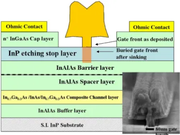
The HEMT structure was grown by molecular beam epi-taxy on a 2-in-diameter InP substrate. The schematic of the structure is shown in Fig. 1 and given as follows. A 50-Å InAs channel layer with 20-Å In0.7Ga0.3As upper subchannel
and 30-Å In0.7Ga0.3As lower subchannel was grown on top
of the 500-nm-thick InAlAs buffer layer. The In0.7Ga0.3As
KUO et al.: PERFORMANCE IMPROVEMENT OF In0.7Ga0.3As/InAs/In0.7Ga0.3As COMPOSITE-CHANNEL HEMT 291
Fig. 1. Schematic view of the device structure. The inserted SEM image is the 80-nm T-shaped gate after recess before silicon nitride passivation.
subchannels were applied to enhance the electron confinement in the thin InAs layer and improve the electron transport prop-erties [10]. A 40-Å-thick InAlAs spacer, a Si-δ-doping with 5× 1012 cm−2, a 10-nm-thick InAlAs barrier, a 4-nm-thick InP etching stop, and a 35-nm-thick InGaAs cap layer with 2× 1018cm−3Si-doping were grown on top of the composite-channel layers.
For the device fabrication, the active area of the device was isolated by wet etch. The ohmic contacts were formed with 3-µm source–drain spacing by evaporating Au/Ge/Ni/Au on heavily doped n-InGaAs cap layer and then alloyed at 250◦C for 25 s to attain low contact resistance (Rc). For the T-shaped gate process, it was performed by the 50-kV JEOL electron beam lithography system (JBX 6000 FS) with trilayer e-beam resist. Succinic acid/H2O2/NH4OH solution was used
for gate recess, and then, Pt (12 nm)/Ti (60 nm)/Pt (80 nm)/Au (180 nm) were deposited as Schottky gate metal and lifted off by ZDMAC to form an 80-nm T-shaped gate. The inserted SEM image is the unpassivated T-shaped gate formed after recess. A 100-nm-thick silicon nitride was deposited as a passivation layer by plasma-enhanced chemical vapor deposition at 250◦C for 10 min. Finally, thermal annealing at 250◦C for 3 min in forming gas ambient was carried out for gate sinking to further recess the channel. The contact resistance was 0.032 Ω· mm after gate-sinking process, which remained almost unchanged as compared with that of 0.021 Ω· mm before annealing.
III. RESULTS ANDDISCUSSION
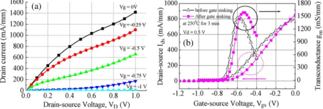
Fig. 2(a) shows the dc I–V curve of the device with 2× 50 µm gate width using gate-sinking technology. The device exhibited a very good pinch-off characteristic and the saturation current of 1418 mA/mm at Vds= 1 V and Vgs= 0 V. This
very high drain–current density was mainly due to the superior electron mobility in the In0.7Ga0.3As/InAs/In0.7Ga0.3As
com-posite channel and the nondegrading performance of the ohmic contact during gate annealing. As for the gate–drain breakdown voltage (VDG,BR), the value decreased from 3.6 V for device
without sinking to 2.4 V for that with sinking, which is mainly
due to the reduction in the Schottky barrier thickness after the gate-sinking process.
The transconductance gmand the drain–source current plot-ted as functions of Vgs for devices without and with gate
annealing are shown in Fig. 2(b). As is observed from the figure, the peak gmvalue has increased from 1470 mS/mm for the device without gate sinking to 1590 mS/mm for that with gate sinking, both measured at Vds= 0.5 V. This increase is
mainly attributed to the sinking of Pt atoms into the InP etching-stop layer which, in turn, shifted the gate metal front closer to the 2-D electron-gas channel. Meanwhile, the threshold voltage shifted from −0.91 (without gate sinking) to −0.8 V (with gate sinking) when biased at Vds= 0.5 V. The threshold
voltage is defined as the Vgs when Ids reaches 1 mA/mm. A
slight reduction in the gate leakage current from 1.66× 10⁻⁶A (without gate sinking) to 6.3× 10⁻⁷A (with gate sinking) was also observed when biased at Vds= 0.8 V and Vgs= 0 V,
owing to the increase in the thickness of the amorphous layer under gate which diminished the leakage path because of the reduction of the grain boundaries [8], [11].
The S parameters of the 2× 50 µm device were mea-sured from 5 to 80 GHz using on-wafer probing system with HP8510XF network analyzer. Fig. 3(a) shows the frequency de-pendence of the current gain H21, the power gain MAG/MSG,
and the Mason’s unilateral gain U of the device with gate sinking measured at Vds= 0.8 V and Vgs=−0.5 V. The
par-asitic effects (mainly capacitive) due to the probing pads have been carefully removed from the measured S parameters using the same method as in [12] and the equivalent circuit model in [13]. Since the geometry of the probing pads is relatively large compared with the device itself, the S parameters of the open probing pads have been carefully characterized through full-wave electromagnetic simulations with measurement. The capacitance at the gate–source end was extracted to be 10.2 fF, and the capacitance at the gate–drain end was about 8.6 fF. A very high current-gain cutoff frequency fT of 494 GHz and the maximum oscillation frequency fmax of 390 GHz were
obtained for device with sinking as compared with that of
fT = 390 GHz and fmax= 360 GHz for the device without
sinking. This improvement in the RF performance was due to the increase of gm and the decrease of the gate-to-source capacitance (Cgs) in the applied gate bias range resulting from
the gate-sinking process. Similar trend of the reduction in Cgs
values due to the gate-sinking process has also been observed in [14]. Table I summarizes the extracted intrinsic parameters for devices with and without gate sinking at the same bias conditions. The increase in fT is mainly caused by the decrease of Cgsand the increase of the transconductance.
The effect of gate sinking on the gate-delay performance of the HEMT device is also evaluated. To avoid erroneous and physically meaningless values of logic parameters in charac-terizing such nonoptimized threshold-voltage device, we have followed the method proposed in [15]. A subthreshold slope of 115 mV/dec and a drain-induced barrier lowering (DIBL) of 200 mV/V after gate sinking were obtained. For device without gate sinking, the subthreshold slope and the DIBL were 115 mV/dec and 178 mV/V, respectively. Fig. 3(b) shows the calculated intrinsic gate delay (CV /I) as a function of
292 IEEE ELECTRON DEVICE LETTERS, VOL. 29, NO. 4, APRIL 2008
Fig. 2. (a) Drain–source current versus drain–source voltage curve. (b) Transconductance versus gate–source voltage before and after gate sinking at 250◦C for 3 min.
Fig. 3. (a) Frequency dependence of the current gain H21, the power gain MAG/MSG, and the unilateral gain U of the InAs/In0.7Ga0.3As composite-channel
HEMTs. The frequency range was from 5 to 80 GHz, and the device was biased at Vds= 0.8 V and Vgs=−0.5 V. (b) Calculated intrinsic gate delay as a
function of ION/IOFFratio with various choices of the threshold voltage for device with and without sinking.
TABLE I
SUMMARY OF THEHEMT DEVICEPARAMETERSWITH ANDWITHOUTGATESINKING
ION/IOFF ratio for the device with and without gate sinking
and with various choices of the threshold voltage as defined in [16] at Vds= 0.6 V. As is observed from the figure, a low
calculated gate delay of 0.78 ps for gate-sinking device with
ION/IOFFratio maintained on the order of 103 was achieved
as compared with that of 0.83 ps for the device without gate sinking. The very low intrinsic gate-delay performance is again attributed to the decrease in the Cgs after the gate-sinking
process. These superior performances have also made such device a potential candidate for future high-speed and low-power logic applications.
IV. CONCLUSION
In this letter, the use of the Pt buried-gate technology for the enhancement of the RF and logic performance of the HEMTs has been demonstrated. The HEMTs exhibit high Ids= 1418 mA/mm, high gm= 1590 mS/mm, and an
fT(fmax) of 494 GHz (390 GHz) after gate sinking. This is
believed to be the highest value ever achieved for an 80-nm
HEMT devices. Additionally, the logic performance of such device has also been characterized, and a very low intrinsic gate delay (0.78 ps) with an ION/IOFFratio in the excess of 103was
obtained at Vds= 0.6 V. Overall, the performance
improve-ment after gate sinking was mainly attributed to the increase of gm and the decrease in the corresponding capacitances of the device. The results demonstrate that superior HEMT device performance for high-frequency, high-speed, and low-power logic applications can be achieved through a very simple gate-sinking process with optimal epitaxy structure.
REFERENCES
[1] K. Shinohara, Y. Yamashita, A. Endoh, K. Hikosaka, T. Matsui, T. Mimura, and S. Hiyamizu, “Extremely high-speed lattice-matched InGaAs/InAlAs high electron mobility transistors with 472 GHz cut-off frequency,” Jpn. J. Appl. Phys., vol. 41, no. 4B, pp. L437–L439, Apr. 2002.
[2] Y. Yamashita, A. Endoh, K. Shinohra, K. Hikosaka, T. Matsui, S. Hiyamizu, and T. Mimura, “Pseudomorphic In0.52Al0.48As/
In0.7Ga0.3As HEMTs with an ultrahigh fTof 562 GHz,” IEEE Electron
KUO et al.: PERFORMANCE IMPROVEMENT OF In0.7Ga0.3As/InAs/In0.7Ga0.3As COMPOSITE-CHANNEL HEMT 293
[3] D. H. Kim, J. A. Alamo, J. H. Lee, and K. S. Seo, “Performance evaluation of 50 nm In0.7Ga0.3As HEMTs for beyond-CMOS logic applications,”
in IEDM Tech. Dig., 2005, pp. 767–770.
[4] R. Chau, S. Datta, and A. Majumdar, “Opportunities and challenges of III–V nanoelectronics for future high-speed, low-power logic applica-tions,” in Proc. IEEE CSIC Dig., 2005, pp. 17–20.
[5] K. Shinohara, Y. Yamashita, A. Endoh, I. Watanabe, K. Hikosaka, T. Matsui, T. Mimura, and S. Hiyamizu, “547 GHz ft In0.7Ga0.3As/
In0.52Al0.48As HEMTs with reduced source and drain resistance,” IEEE
Electron Device Lett., vol. 25, no. 5, pp. 241–243, May 2004.
[6] H. Matsuzaki, T. Maruyama, T. Kosugi, H. Takahashi, M. Tokumitsu, and T. Enoki, “Laterally scaled down tiered-edge ohmic structure of InP-based HEMTs for 2 S/mm gmand 500 GHz fT,” in IEDM Tech. Dig., 2005,
pp. 775–778.
[7] K. J. Chen, T. Enoki, K. Arai, and M. Yamamoto, “High-performance InP-based enhancement-mode HEMTs using non-alloyed ohmic contacts and Pt-based buried-gate technologies,” IEEE Trans. Electron Devices, vol. 43, no. 2, pp. 252–257, Feb. 1996.
[8] L. H. Chu, E. Y. Chang, L. Chang, Y. H. Wu, S. H. Chen, H. T. Hsu, T. L. Lee, Y. C. Lien, and C. Y. Chang, “Effect of gate sinking on the device performance of the InGaP/AlGaAs/InGaAs enhancement-mode PHEMT,” IEEE Electron Device Lett., vol. 28, no. 2, pp. 82–85, Feb. 2007.
[9] N. Harada, S. Kuroda, T. Katakami, K. Hikosaka, T. Mimura, and M. Abe, “Pt-based gate enhancement-mode InAlAs/InGaAs HEMTs for large-scale integration,” in Proc. 3rd Int. Conf. InP Related Mater., 1991, pp. 377–380.
[10] T. Akazaki, K. Arai, T. Enoki, and Y. Ishii, “Improved InAlAs/InGaAs HEMT characteristics by inserting an InAs layer into the InGaAs channel,” IEEE Electron Device Lett., vol. 13, no. 6, pp. 325–327, Jun. 1992.
[11] D. H. Ko and R. Sinclair, “Amorphous phase formation in an as-deposited platinum-GaAs interface,” Appl. Phys. Lett., vol. 58, no. 17, pp. 1851– 1853, Apr. 29, 1991.
[12] Y. Yamashita, A. Endoh, K. Shinohara, M. Higashiwaki, K. Hikosaka, T. Mimura, S. Hiyamizu, and T. Matsui, “Ultra-short 25 nm gate lattice match InAlAs/InGaAs HEMTs within the range of 400 GHz cut off frequency,” IEEE Electron Device Lett., vol. 22, no. 8, pp. 367–369, Aug. 2001.
[13] G. Dambrine, A. Cappy, F. Heliodore, and E. Playez, “A new method for determining the FET small-signal equivalent circuit,” IEEE Trans. Microw. Theory Tech., vol. 36, no. 7, pp. 1151–1159, Jul. 1988. [14] S. Kim, I. Adesida, and H. Hwang, “Measurements of the thermally
induced nanometer-scale diffusion depth of Pt/Ti/Pt/Au gate metallization on InAlAs/InGaAs high-electron mobility transistors,” Appl. Phys. Lett., vol. 87, no. 23, p. 232 102, Dec. 2005.
[15] R. Chau, S. Datta, M. Doczy, B. Doyle, B. Jin, J. Kavalierous, A. Majumdar, M. Metz, and M. Radosavljevic, “Benchmarking nan-otechnology for high-performance and low-power logic transistor ap-plications,” IEEE Trans. Nanotechnol., vol. 4, no. 2, pp. 153–158, Mar. 2005.
[16] J. Guo, A. Javey, H. Dai, and M. Lundstrom, “Performance analysis and design optimization of near ballistic carbon nano tube field effect transistors,” in IEDM Tech. Dig., 2004, pp. 703–706.