Thermomigration in flip-chip SnPb solder joints under alternating current stressing
Hsiang-Yao Hsiao and Chih Chen
Citation: Applied Physics Letters 90, 152105 (2007); doi: 10.1063/1.2721136
View online: http://dx.doi.org/10.1063/1.2721136
View Table of Contents: http://scitation.aip.org/content/aip/journal/apl/90/15?ver=pdfcov Published by the AIP Publishing
Articles you may be interested in
Erratum: “Thermomigration in flip-chip SnPb solder joints under alternate current stressing” [Appl. Phys. Lett.90, 152105 (2007)]
Appl. Phys. Lett. 90, 249902 (2007); 10.1063/1.2748851
Effect of entropy production on microstructure change in eutectic SnPb flip chip solder joints by thermomigration Appl. Phys. Lett. 89, 221906 (2006); 10.1063/1.2385205
Effect of the combination of electromigration and thermomigration on phase migration and partial melting in flip chip composite SnPb solder joints
J. Appl. Phys. 100, 033512 (2006); 10.1063/1.2227621 Thermomigration in SnPb composite flip chip solder joints Appl. Phys. Lett. 88, 141911 (2006); 10.1063/1.2192694
Thermomigration in Pb–Sn solder joints under joule heating during electric current stressing Appl. Phys. Lett. 82, 1045 (2003); 10.1063/1.1554775
This article is copyrighted as indicated in the article. Reuse of AIP content is subject to the terms at: http://scitation.aip.org/termsconditions. Downloaded to IP: 140.113.38.11 On: Thu, 01 May 2014 00:33:46
Thermomigration in flip-chip SnPb solder joints under alternating
current stressing
Hsiang-Yao Hsiao and Chih Chena兲
Department of Materials Science and Engineering, National Chiao Tung University, Hsin-chu, Taiwan 30010, Republic of China
共Received 26 January 2007; accepted 8 March 2007; published online 10 April 2007兲
Thermomigration in flip-chip solder joints is investigated using alternating currents and infrared microscopy to decouple it from electromigration effect. It is found that the thermal gradient in solder bump can be as high as 2143 ° C / cm when 9.2⫻104A / cm2 was applied at 100 ° C. Markers fabricated by focus ion beam are employed to measure the thermomigration rate. The thermomigration flux is measured to be 3.3⫻1013at./ cm2. With the known thermal gradient, the molar heat of 26.8 kJ/ mole has been obtained for the transport of Pb. © 2007 American Institute of
Physics. 关DOI:10.1063/1.2721136兴
Electromigration in flip-chip solder joints has attracted a lot of attention in recent years due to the miniaturization trend in high-performance devices.1As the current density in solder bump continues to increase, the electromigration be-comes an inevitable reliability issue in solder joints. During electromigration test, thermomigration also occurs under se-vere stressing conditions.2–4Since Al traces act as the major Joule heating source,5,6the solder close to the chip is hotter than that near the substrate, creating a thermal gradient across the solder bump, thus driving the motion of Sn and Pb atoms. Ye et al. performed a simulation and reported that the thermal gradient in the solder joint may be as high as 1500 ° C / cm when applied by 1 A.2Huang et al. found that Sn atoms move to the hot end,3while the Pb atoms diffuse to the cold end. They estimated that the thermal gradient needed for thermomigration to occur during electromigration is 1000 ° C / cm. Chuang and Liu created a thermal gradient of up to 1000 ° C / cm in a Cu/ SnPb/ Cu sandwich struc-ture, and the heat of transport was measured to be 22.16 kJ/ mole.4However, there are no experimental data to verify if such a large thermal gradient exists in real flip-chip solder bumps.
In this study, infrared microscopy was employed to mea-sure the thermal gradient directly in cross-sectioned solder joints. An alternating current共ac兲 was applied to the joint to decouple the thermomigration from electromigration effect, since there is no electromigration effect under ac stressing. However, the ac produces the same amount of Joule heating as the direct current dose. In addition, markers indented by focused ion beam共FIB兲 were employed to measure the ther-momigration flux in this experiment. Thus, the molar heat of transport can be obtained.
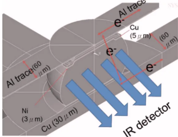
Infrared microscopy was employed to measure the ther-mal gradient in the cross sections of solder bumps under different stressing currents. The experimental setup is shown in Fig.1. The diameter of the eutectic SnPb solder joint was 130m. It had a height of 70m and an under-bump-metallization共UBM兲 opening of 120m in diameter on the chip side. The UBM was electroplated with Ni and Cu. The original dimension of the Al traces on the chip side was
100m wide and 1.5m thick, while the dimension of the Cu lines on FR5 substrates was 25m thick and 100m wide. The pitch in the solder bumps was 1 mm.
To observe the thermomigration in situ, the bumps were polished laterally to approximate their centers. After being polished, the widths of the Al traces and the Cu lines also decreased accordingly. Current stressing was carried out at a temperature of 100 ° C on a hot plate. A constant ac of 0.55 A with a frequency of 45 Hz was passed through two bumps, producing a nominal current density of 9.2⫻104A / cm2in the bumps.
Prior to current stressing, the emissivity of the specimen was calibrated at 100 ° C. After the calibration, the bumps were powered by an alternating current. The temperature was then measured to record the temperature distribution共map兲 after reaching a steady state. The temperatures in the solder joints were mapped by Quantum Focus Instruments thermal infrared microscopy, which has a temperature resolution of 0.1 ° C and a spatial resolution of 2m. The changes in surface microstructure were examined using a scanning elec-tron microscope共SEM兲.
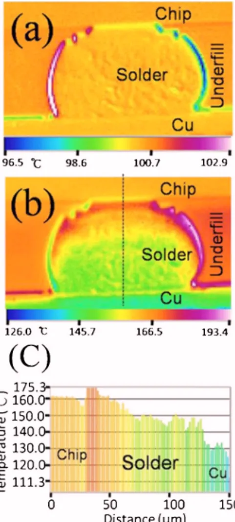
The thermal gradient can exceed 2000 ° C / cm at a higher current density in real flip-chip solder joints. The tem-perature distribution in the bump before current stressing is shown in Fig.2共a兲. The temperature in the solder bump is quite uniform except for the left and right edges of the bump.
a兲Author to whom correspondence should be addressed; electronic mail:
FIG. 1.共Color online兲 Schematic diagram of the experimental setup used in this study.
APPLIED PHYSICS LETTERS 90, 152105共2007兲
0003-6951/2007/90共15兲/152105/3/$23.00 90, 152105-1 © 2007 American Institute of Physics
This article is copyrighted as indicated in the article. Reuse of AIP content is subject to the terms at: http://scitation.aip.org/termsconditions. Downloaded to IP: 140.113.38.11 On: Thu, 01 May 2014 00:33:46
The temperatures on the two edges may not be correct since the image was taken at a long exposure time of 15 s and the sample may vibrate during the time span. When the joint was powered by 0.55 A, the temperature increased nonuniformly, as shown in Fig.2共b兲. The average temperature increases in the bump because the current stressing was as high as 55.6 ° C. The solder near the chip end was hotter since the major Joule heating source was the Al traces on the chip side, which created a thermal gradient across the bump. The thermal gradient is defined here as the difference between average temperature near the substrate end in the bump and that near the chip end in the bump divided by the height of the bump, i.e., 共Tchip− Tsub兲/h. The temperatures near the
chip and substrate ends were obtained by averaging the val-ues in the white rectangles in Fig.2共a兲. Figure2共c兲shows the temperature profile along the dashed line in Fig. 2共b兲, in which the average temperature in the chip end is 16.0 ° C higher than that in the substrate end. The thermal gradient was calculated to be 2143 ° C / cm.
The measured temperature gradients in the bump for various stressing conditions are shown in Fig. 3. The tem-perature gradients increase as the stressing currents increase. The joints may fail instantly when the applied current ex-ceeds 0.6 A. The temperature gradient was as high as
2143 ° C / cm when powered by 0.55 A but only 571 ° C / cm when powered by 0.14 A. The current density required to create a thermal gradient of 1000 ° C / cm was about 5⫻104A / cm2.
Thermomigration behavior becomes severe when the bumps were subjected to a high thermal gradient of 2571 ° C / cm. Figure4共a兲shows the backscattered SEM im-age for the bump before applying the alternating current. After applying 0.55 A at 100 ° C for 108 h, thermomigration damage was observed, as illustrated in Fig.4共b兲. Some of the solders near the chip side have migrated to the substrate side. In addition, phase separation was found. The Pb-rich phase migrated toward the substrate, which was the cold end. These results are in agreement with those reported by Huang
et al.3As shown in Fig.2共b兲, the average temperature in the bump during current stressing was as high as 155 ° C, Pb atoms are the dominant diffusion species. Therefore, more Pb atoms are migrated to the substrate side than the flux of Sn atoms migrating in the opposite direction. Therefore, depletion was observed on the chip side. The other bump that experienced current stressing also exhibited similar behavior, thus it was not shown in this letter.
FIG. 2. 共Color online兲 共a兲 Temperature distribution of the bump before current stressing, showing a uniform temperature distribution in solder;共b兲 temperature distribution in the bump powered by 0.55 A, which corresponds to a current density of 9.2⫻104A / cm2; and共c兲 temperature profile along
the dashed line in 共b兲. The thermal gradient was calculated to be 2571 ° C / cm.
FIG. 3. Measured temperature increases in the bump as a function of ap-plied current and current densities.
FIG. 4. Backscattered SEM images for the bump:共a兲 before current stress-ing and共b兲 after ac stressing by 0.55 A at 100 °C for 108 h. Thermomigra-tion damage occurred obviously.
152105-2 H.-Y. Hsiao and C. Chen Appl. Phys. Lett. 90, 152105共2007兲
This article is copyrighted as indicated in the article. Reuse of AIP content is subject to the terms at: http://scitation.aip.org/termsconditions. Downloaded to IP: 140.113.38.11 On: Thu, 01 May 2014 00:33:46
To measure the thermomigration flux under a specific thermal gradient, seven 0.1m holes were etched by Ga ions in a FIB on the surface of another bump.
The depth of the hole was about 200 nm. The holes were used as markers during thermomigration. Figures 5共a兲 and
5共b兲 show SEM images for the bump with the markers be-fore and after current stressing, respectively. The thermal gradient was measured to be 2143 ° C / cm for this bump un-der the stressing of 0.55 A. The seven markers all moved upwards by a distance of 3.2m after current stressing for 96 h, as the Pb atoms moved downwards. The original marker positions were indicated in Fig.5共b兲.
By measuring the average displacement of the markers ⌬X, the thermomigration JTMcan be obtained using the
fol-lowing equation.
JTM=共A⌬X兲N
MAt , 共1兲
whereis the density of SnPb共8.11 g/cm3兲, M is the atomic weight of SnPb 共136.39 g/mole兲, A is the cross-sectional
area, and t is the stressing time. The average displacement was measured to be 3.2m. Thus, thermomigration flux was calculated to be 3.3⫻1013at./ cm2. In addition, the
thermo-migration flux for the one-dimensional case under a thermal gradient dT / dx can be expressed as5,7
JTM=nDA共Q
*/N兲
kT2
冉
dT
dx
冊
, 共2兲where n is the atomic density, DA is the coefficient of
self-diffusion, k is Boltzmann’s constant, N is Avogadro’s num-ber, dT / dx is the thermal gradient, and T is the temperature.
Q*is a constant, which is called the heat of transport. With the DA data published by Gupta et al.,8 the molar heat flux
Q* can be determined to be 26.8 kJ/ mole. Compared with
the value reported by Chuang and Liu, the value obtained in this study was slightly larger. Their testing conditions were 80– 110 ° C on eutectic SnPb alloy, and the value they ob-tained was about 22.16 kJ/ mole.
In summary, by using alternating currents, the thermo-migration effect can be investigated independently. A very large thermal gradient exceeding 2143 ° C / cm can be de-tected at a high current density with the aid of an infrared microscope. Pb atoms were found to diffuse to the cold end under a current stressing of 0.55 A. From the displacement of markers, the thermomigration flux can be measured to be 3.3⫻1013at./ cm2. With the measured flux and thermal
gra-dient, the molar heat of transport of Pb has been calculated to be 26.8 kJ/ mole.
The authors would like to thank the National Science Council of R.O.C. for the financial support of this study through Grant No. 95-2218-E-009-022.
1K. N. Tu, J. Appl. Phys. 94, 5451共2003兲.
2H. Ye, C. Basaran, and D. C. Hopkins, Appl. Phys. Lett. 82, 1045共2003兲. 3Annie T. Huang, A. M. Gusak, and K. N. Tu, Appl. Phys. Lett. 88, 141911
共2006兲.
4Y. C. Chuang and C. Y. Liu, Appl. Phys. Lett. 88, 174105共2006兲. 5S. W. Liang, Y. W. Chang, and Chih Chen, Appl. Phys. Lett. 88, 172108
共2006兲.
6S. H. Chiu, T. L. Shao, and Chih Chen, Appl. Phys. Lett. 88, 022110
共2006兲.
7Y. Adda and J. Philibert, Solid State Phys. 22, 409共1986兲. 8D. Gupta, K. Vieregge, and W. Gust, Acta Mater. 5, 47共1999兲.
FIG. 5. SEM images for the bump with seven markers:共a兲 before current stressing and共b兲 after current stressing by 0.55 A at 100 °C for 108 h. All the markers moved upwards after ac stressing.
152105-3 H.-Y. Hsiao and C. Chen Appl. Phys. Lett. 90, 152105共2007兲
This article is copyrighted as indicated in the article. Reuse of AIP content is subject to the terms at: http://scitation.aip.org/termsconditions. Downloaded to IP: 140.113.38.11 On: Thu, 01 May 2014 00:33:46