附件一
行政院國家科學委員會補助專題研究計畫
□ 成 果 報 告
□期中進度報告
V介觀系統的自旋抽運與電荷抽運(1/3)
計畫類別:□ 個別型計畫 □ 整合型計畫
計畫編號:NSC 93 - 2112 - M - 009 - 017 -
執行期間: 2005 年 08 月 01 日至 2006 年 07 月 31 日
V計畫主持人:朱仲夏 教授
共同主持人:
計畫參與人員:M. Büttiker, P. Samuelsson, Mal’shukov,K. A. Chao,
唐志雄, 鄔其君, 鍾淑維,王律堯, 張榮興, 陳冠伊
成果報告類型(依經費核定清單規定繳交):□精簡報告 □完整報告
V本成果報告包括以下應繳交之附件:
□赴國外出差或研習心得報告一份
□赴大陸地區出差或研習心得報告一份
□出席國際學術會議心得報告及發表之論文各一份
□國際合作研究計畫國外研究報告書一份
處理方式:除產學合作研究計畫、提升產業技術及人才培育研究計畫、
列管計畫及下列情形者外,得立即公開查詢
□涉及專利或其他智慧財產權,□一年□二年後可公開查詢
執行單位:國立交通大學電子物理系
中 華 民 國 95 年 5 月 30 日
行政院國家科學委員會專題研究計劃成果報告
介觀結構的量子傳輸: (一) 應力感應與自旋流耦合產生之奈米機械震盪;(二) 對電子式 Mach-Zehnder 干涉儀和電子式 Hanbury Brown Twiss 干涉儀作電流及雜訊干涉度的分 析;(三)在 Rashba-type 量子窄通道產生自旋流;(四) 在 Rashba-type 窄通道中雜質效應對 於產生直流自旋流之影響; (五) 自旋霍爾效應對二維條狀半導體的邊緣磁化強度以及電導 的影響;(六) 兩個接腳的介觀環在傳輸下的 Fano 效應;(七)一維系統的三腳接點之波函數 連結; (八) 在本質自旋霍爾效應下在彈性散射體附近感應出自旋雲。
The quantum transport in mesoscopic structure: [ I ] Strain induced coupling of spin current to nanomechanical oscillations; [ II ] Visibility of current and shot noise in electrical Mach-Zehnder and Hanbury Brown Twiss interferometers; [ III ] dc spin current generation in a Rashba-type quantum channel; [IV] Effects of elastic scatterer on the dc spin current generation in a Rashba-type channel; [V] Spin Hall Effect on Edge Magnetization and Electric conductance of a 2D Semiconductor Strip; [ VI ] Fano resonance in transport through a mesoscopic two-lead ring; [VII] Connecting wave functions at a three-legs junction of one-dimensional channels; [VIII] Spin cloud induced around an elastic scatterer by the intrinsic spin-Hall effect.
一、中文摘要:
在本計劃中,我們研究了介觀系統的自旋抽運與電荷抽運(2/3),其中包括(一) 應力感 應與自旋流耦合產生之奈米機械震盪;(二) 對電子式 Mach-Zehnder 干涉儀和電子式 Hanbury Brown Twiss 干涉儀作電流及雜訊干涉度的分析;(三)在 Rashba-type 量子窄通道 產生自旋流;(四) 在 Rashba-type 窄通道中雜質效應對於產生直流自旋流之影響; (五) 自 旋霍爾效應對二維條狀半導體的邊緣磁化強度以及電導的影響;(六)兩個接腳的介觀環在傳 輸下的 Fano 效應;(七)一維系統的三腳接點之波函數連結;(八)在本質自旋霍爾效應下在 彈性散射體附近感應出自旋雲。 (一) 我們提出不用靠鐵磁材料而達到電子自旋與奈米機械系統之機械運動耦合之效 應。 這種方法會在 narrow gap 半導體材料中,因應力而感應出自旋軌道交互作用而這種方 式可透過奈米機械元件所形成的懸空棒狀結構以去偵測和操控自旋流。 (二)利用 ac 閘極來 產生和量測自旋流:我們研究在III-V 族窄能隙的量子阱或量子線中,可以利用一個時變的 閘極去影響Rashba 自旋軌道耦合係數來產生自旋流。我們也提出對此交流自旋流的整流方 法,以及利用電性量測去測量在二維電子氣中帶有交流自旋流的閘極附近的電壓以達到偵 測自旋流之目的;我們提出一種不需要使用光學或磁性材料來達到”產生”和”偵測”自旋流 的方法。
(二) 本研究針對電子式 Mach-Zehnder 干涉儀和電子式 Hanbury Brown Twiss 干涉儀作 電流及雜訊干涉度的分析。此電子式干涉儀是利用高磁場下電子沿著導体的邊通道(edge
states)運動特性所做成。傳輸的特性可藉由 Aharonov-Bohm flux 來調整。我們研究環境溫度
及外加偏壓對電流及雜訊干涉度的影響。Dephasing 效應是由虛探針模型來模擬。比較兩電
子式干涉儀是有趣的,因為Mach-Zehnder 干涉儀是電子振幅(單粒子)干涉儀,然而 Hanbury
Brown Twiss 干涉儀是電子強度(雙粒子)干涉儀。若要做直接的比較,只能經由量測雜訊。 我們發現Hanbury Brown Twiss 干涉儀中的雜訊干涉度對環境溫度、外加電壓及 dephasing
的反應是大約相似於Mach-Zehnder 干涉儀的第一諧波雜訊干涉度。相對的,Mach-Zehnder 干涉儀的第二諧波雜訊干涉度被環境溫度、外加偏壓及dephasing rate 的影響高於第一諧波 雜訊干涉度。 (三)共振非彈性散射對於直流自旋流的產生扮演重要的角色,共振非彈性散射使得單一 交流偏壓指狀閘極橫跨在具有Rashba自旋軌道的量子窄通道中產生自旋流,此交流偏壓的指 狀閘極使Rashba耦合係數隨時間震盪變化,造成自旋相關的共振非彈性散射機制,自旋流 產生必須同時存在靜態的與動態的Rashba偶合係數,而自旋流正比α0α12,由於結構對稱所 以並不會產生直流電流,我們也可以利用兩個指狀閘極來增強自旋流強度。 (四) 我們探討在 Rashba-type 窄通道中雜質對直流自旋流的影響,此直流自旋流可由單 一交流指狀閘極所產生而且不會伴隨直流電流,此彈性散射源對直流自旋流有重要影響, 我們考慮橫向均勻的位壘產生的反彈散射機制;而對於橫向不均勻位壘會產生反彈散射和 能帶混成的效果,我們也比較的吸引和排斥性的非均勻位能對自旋流的影響,對於吸引性 的位壘而言,在不同能帶交錯點附近會產生額外的結構,這是由於 inter-subband 間的躍 遷到能帶底部形成準束縛態造成的結果。 (五)我們研究二維擴散系統下,變化二維條狀系統的寬度,探討本質自旋霍爾效應對於 自旋累積和電導的影響;結果顯示當縱向穩態電流流動時,條狀樣品邊緣對於自旋極化出 現阻尼震盪的行為,此一結果與樣品寬度和 Dresselhaus 自旋軌道偶合強度有關聯,對於 自旋累積,三次方的交互作用項是非常重要的,如預期一般,對於 Rashba 自旋軌道交互作 用並無此一自旋累積的情形發生。 (六) 兩接頭的介觀環的 Fano 共振傳輸的研究:我們研究在無外加磁場情況下有兩個 接頭的一維介觀環的傳輸現象;我們研究集中在環中的位能並沒有規範出一個封閉性共振 腔或是封閉性量子點的例子,即使在沒有良好定義的準束縛態下,我們依然發現穿透係數 出現Fano 結構;這些 Fano 結構出現是由於符合環的駐波條件,他們對於系統參數的對稱 性相當敏感。當系統完全對稱時,Fano 結構變成無限窄,此一結果告訴我們對於一般 Fano 結構是因為連續能量的粒子穿透一分立的共振能階所產生的干涉現象結果,值得商榷。 (七) 一維系統的三腳接點之波函數連結:我們提出一種方法去處理一維分支的三接腳 (Y 型接腳)結構中,波函數如何去連接;我們的結果不同於 Griffiths 的結論[Trans. Faraday Soc. 49, 345 (1953)],我們的模型可以處理不同寬度的準一維接腳結構,我們用我們的方法去比 較在一維和準一維系統下都得到不錯的擬合,因此此一模型對於描述準一維結構是相當有 用的。
(八)在本質自旋霍爾效應下在彈性散射體附近感應出自旋雲: 類比於電流流過雜質實
產生Landauer 電偶極矩,由於本質自旋霍爾效應,在自旋無關的散射體附近也會感應出墊
子自旋雲,在彈道傳輸的範疇內,在Rashba 自旋軌道交互作用下,不會產生自旋霍爾電流,
但也會感應出自旋雲。
Abstract:
We study the spin and charge pumping in mesoscopic structures: [ I ] Strain induced coupling of spin current to nanomechanical oscillations; [ II ] Visibility of current and shot noise in electrical Mach-Zehnder and Hanbury Brown Twiss interferometers; [ III ] dc spin current generation in a Rashba-type quantum channel; [IV] Effects of elastic scatterer on the dc spin current generation in a Rashba-type channel; [V] Spin Hall Effect on Edge Magnetization and Electric conductance of a 2D Semiconductor Strip; [ VI ] Fano resonance in transport through a mesoscopic two-lead ring; [VII] Connecting wave functions at a three-legs junction of one-dimensional channels; [VIII] Spin cloud induced around an elastic scatterer by the intrinsic spin-Hall effect.
.
[I] Strain induced coupling of spin current to nanomechanical oscillations:
We propose a setup which allows to couple the electron spin degree of freedom to the mechanical motions of a nanomechanical system not involving any of the ferromagnetic components. The proposed method employs the strain induced spin-orbit interaction of electron in narrow gap semiconductors. We have shown how this method can be used fro detection and manipulation of the spin flow through a suspended rod in a nanomechanical device.
[II] Visibility of current and shot noise in electrical Mach-Zehnder and Hanbury Brown Twiss interferometers :
We investigate the visibility of the current and shot-noise correlations of electrical analogs of the optical Mach-Zehnder interferometer and the Hanbury Brown Twiss interferometer. The electrical analogs are discussed in conductors subject to high magnetic fields where electron motion is along edge states. The transport quantities are modulated with the help of an Aharonov-Bohm flux. We discuss the conductance (current) visibility and shot noise visibility as a function of temperature and applied voltage. Dephasing is introduced with the help of fictitious voltage probes. Comparison of these two interferometers is of interest since the Mach-Zehnder interferometer is an amplitude (single-particle) interferometer whereas the Hanbury Brown Twiss interferometer is an intensity (two-particle) interferometer. A direct comparison is only possible for the shot noise of the two interferometers. We find that the visibility of shot noise correlations of the Hanbury Brown Twiss interferometer as function of temperature, voltage or dephasing, is qualitatively similar to the visibility of the first harmonic of the shot noise correlation of the Mach-Zehnder interferometer. In contrast, the second harmonic of the shot noise visibility of the Mach-Zehnder interferometer decreases much more rapidly with increasing temperature, voltage or dephasing rate.
[III] dc spin current generation in a Rashba-type quantum channel:
We propose and demonstrate theoretically that resonant inelastic scattering _RIS_ can play an important role in dc spin current generation. The RIS makes it possible to generate dc spin current via a simple gate configuration: a single finger gate that locates atop and orients transversely to a quantum channel in the presence of Rashba spin-orbit interaction. The ac-biased finger gate gives rise to a time variation in the Rashba coupling parameter, which causes spin-resolved RIS and, subsequently, contributes to the dc spin current. The spin current depends on both the static and the dynamic parts in the Rashba coupling parameter, α0 and α1,
respectively, and is proportional to α0α12 The proposed gate configuration has the added
advantage that no dc charge current is generated. Our study also shows that the spin current generation can be enhanced significantly in a double finger-gate configuration.
[IV] Effects of impurity on the dc spin current generation in a Rashba-type channel:
We have investigated the effects of a single impurity on the dc spin current (SC) generation in a Rashba-type channel. The dc SC could be generated via a single ac finger-gate (FG). Effects of impurity have strong dependence of transverse-location and strength for the transport of dc SC in the channel. The spin-resolved dip structures are broadened while the impurity is away from the edge inside of the ac-FG. The effect of impurity is decreased for the impurity in the edge of the channel. The impurity has small effect for the transport while the impurity is outside of the ac-FG. The spin-resolved inter-subband transition is observed while the incident energy near each subband threshold because the symmetry of transverse direction is broken by the impurity.
[V]Spin Hall Effect on Edge Magnetization and Electric Conductance of a 2D semiconductor Strip:
The intrinsic spin Hall effect on spin accumulation and electric conductance in a diffusive regime of a 2D electron gas has been studied for a 2D strip of a finite width. It is shown that the spin polarization near the flanks of the strip, as well as the electric current in the longitudinal direction, exhibit damped oscillations as a function of the width and strength of the Dresselhaus spin-orbit interaction. Cubic terms of this interaction are crucial for spin accumulation near the edges. As expected, no effect on the spin accumulation and electric conductance have been found in case of Rashba spin-orbit interaction.
[VI] Fano resonance transport through a mesoscopic two-lead ring:
The ballistic transport through a one-dimensional two-lead ring at zero magnetic field is studied. We have focused on the case in which the potential in the ring does not define closed cavities or dots. Even in the absence of well-defined quasibound states, we find Fano profiles in the transmission probability. Those Fano profiles appear at energies corresponding to the standing-wave states in the ring, but their occurrence depends sensitively on the commensurability of the system parameters. When the system parameters are commensurate, the widths of the profiles at some energies are infinitesimally small. These findings suggest that the conventional understanding of the Fano profiles as a result of the interference effect of the
transition through resonant states and nonresonant continuum of states, might not account for all the Fano profiles seen in the transport measurements. Moreover, the sensitivity and tunability of the resonance with respect to the system parameters may be usable in the fabrication of electrical nanodevices.
[VII] Connecting wave functions at a three-leg junction of one-dimensional channels:
We propose a scheme to connect the wave functions on different one-dimensional branches of a three-leg junction _Y junction_. Our scheme differs from that due to Griffith [Trans. Faraday Soc. 49, 345 (1953)] in the respect that ours can model the difference in the widths of the quasi-one-dimensional channels in different systems. We test our scheme by comparing results from a doubly connected one-dimensional system and a related quasi-one-dimensional system, and we find a good agreement. Therefore our scheme may be useful in the construction of one-dimensional effective models out of _multiply connected_ quasi-one-dimensional systems. [VIII] Spin cloud induced around an elastic scatterer by the intrinsic spin-Hall effect:
Similar to the Landauer electric dipole created around an impurity by the electric current, a spin polarized cloud of electrons can be induced by the intrinsic spin-Hall effect near a spin independent elastic scatterer. It is shown that in the ballistic range around the impurity, such a cloud appears in the case of Rashba spin-orbit interaction, even though the bulk spin-Hall current is absent.
Keywords:
Quantum transport, quasi-bound state, inelastic scattering, quantum channel, spin current, Spin Hall Effect, Spin accumulation, spin cloud, Rashba spin-orbit interaction, Dresselhau spin-orbit interaction, mesoscopic ring, Fano structures, persistent current, current visibility, noise visibility, Mach-Zehnder interferometer, the Hanbury Brown Twiss interferometer, edge states, Aharonov-Bohm flux, dephasing, Fano effect.
二、Motivations and goals
[I] Strain induced coupling of spin current to nanomechanical oscillations:
An ability to control the spin transport in semiconductors is a key problem to be solved towards implementation of semiconductor spintronics into quantum information processing [1-3]. Many methods have been proposed to achieve control of the electron spin degree of freedom using magnetic materials, external magnetic fields and optical excitation [3]. Other promising ideas involve the intrinsic spin-orbit interaction (SOI) in narrow gap semiconductors to manipulate the spin by means of electron fields [4] and electric gates [5-7]. Recently, some of these ideas have been experimentally confirmed [8,9].
In semiconductors the spin-orbit effect appears as an interaction of the electron spin with an effective magnetic field whose direction and magnitude depend on the electron momentum. A specific form of this dependence is determined by the crystal symmetry, as well as by the symmetry of the potential energy profile in heterostructures. In strained semiconductors new components of the effective magnetic field appear due to violation of the local crystal symmetry [10]. The effective of the strain induced SOI on spin transport was spectacularly demonstrated by Kato et. al. in their Faraday rotation experiment [9]. An interesting property of the strain induced SOI is that the strain can be associated with mechanical motion of the solid, in particular, with oscillations in nanomechanical systems (NMS), in such a way making possible the spin-orbit coupling of the electron spin to nanomechanical oscillations. At the same time a big progress in fabricating various NMS [11] allows one to reach the required parameter range to observe subtle effects produced by such a coupling.
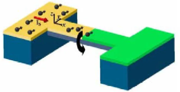
We will consider NMS in the form of a suspended beam with a doped semiconductor film epitaxially grown on its surface (see Fig. 1). An analysis of the SOI in this system shows that the flexural and torsion vibrational modes couple most effectively to the electron spin. As a simple example, we will focus the torsion modes. The strain associated with torsion produces the spin-orbit field which is linear with respect to the electron momentum and is directed perpendicular to it. This field varies in time and space according to respective variations of the torsion strain. Due to the linear dependence on the momentum, the SOI looks precisely as interaction with spin dependent electromagnetic vector potential. An immediate result of this analogy is that the time dependent torsion gives rise to a motive force on electrons. Such a force, however, acts in different directions on particles with oppositely oriented spins, including thus the spin current in the electron gas. The physics of this phenomenon is very similar to the spin current generation under time dependent Rashba SOI, where the time dependence of the SOI coupling parameter is provided by the gate voltage variation [6]. In the present work we will focus, however, on the inverse effect. Due to the SOI coupling, the spin current flowing through the beam is expected to create a mechanical torsion. The torque effect on NMS due to spin flow has been previously predicted [12] for a different physical realization, where the torque has been created by spin flips at nonmagnetic-ferromagnetic interface. They also suggested an experimental set up to measure such a small torque. The torque due to SOI effect can be by 2 orders of magnitude stronger than the torque produced by the current flowing through the FM-NM interface. Hence, the SOI effect can be measured by the same method as was proposed [12]. Besides this method, other sensitive techniques for displacement measurements can be
employed [13].
Fig. 1 : Schematic illustration of electromechanical spin current detector, containing a suspended semiconductor-mental (S-M) rectangular rod atop an insulating substrate (blue). A spin current is injected from the left semiconductor reservoir (yellow) and then diffuses toward the metallic film (green). While passing through the semiconductor film, the spin current induces torque shown by the black arrow.
[Reference]:
[1] Semiconductor Spintronics and Quantum Computation, edited by D. D. Awschalom, N. Samarth, and D. Loss (Springer-Verlag, Berlin, 2002).
[2] S. A.Wolf, et. al., Science. 294, 1488 (2001).
[3] I. Žutić, J. Fabian, and S. Das Sarma, Rev. Mod. Phys. 76, 323 (2004).
[4] J. Sinova, et. al., Phys. Rev. Lett. 92, 126603 (2004); S. Murakami, N. Nagaosa and S. Zhang, Science 301, 1348 (2003); V. M. Edelstein, Solid State Commun., 73, 233 (1990); A. Voskoboynikov, et. al., Phys. Rev. B. 59, 12514 (1999); L. S. Levitov and E. I. Rashba, Phys. Rev. B, 67, 115324 (2003).
[5] S. Datta and B. Das, Appl. Phys. Lett. 56, 665 (1990); P. Sharma and P. W. Brouwer, Phys. Rev. Lett. 91, 16 6801 (2003); M. Governale, F. Taddei, and R. Fazio, Phys. Rev. B, 68, 155324 (2003).
[6] A. G. Malshukov, et. al., Phys. Rev. B, 68, 23 3307 (2003); C. S. Tang, A. G. Malshukov, and K.A. Chao, cond-mat/0412181.
[7] C. S. Tang, A. G. Mal’shukov, and K. A. Chao, Phys.Rev. B 71, 195314 (2005). [8] J. Wunderlich, B. Kästner, J. Sinova, and T. Jungwirth, cond-mat/0410295. [9] Y. K. Kato, et. al., cond-mat/0502627.
[10] G. E. Pikus and A. N. Titkov, in Optical Orientation, edited by F. Meier and B. P. Zakharchenya (North-Holland, Amsterdam, 1984).
[11] M. L. Roukes, Phys. World 14, 25 (2001); H. G. Craighead, Science 290, 1532 (2000); A. N. Cleland, Foundations of Nanomechanics (Springer, New York, 2003).
[12] P. Mohanty, G. Zolfagharkhani, S. Kettemann, and P. Fulde, Phys. Rev. B 70, 195301 (2004).
[II] Visibility of current and shot noise in electrical Mach-Zehnder and Hanbury Brown Twiss interferometers:
With the advent of mesoscopic physics, it has become possible to experimentally investigate quantum phase coherent properties of electrons in solid state conductors in a controlled way. In particular, in ballistic mesoscopic samples at low temperatures, electrons can propagate up to several microns without loosing phase information. This opens up the possibility to investigate electrical analogs of various optical phenomena and experiments. An investigation of such analogs is of fundamental interest. On the one hand, it allows one to establish similarities between the properties of photons and conduction electrons, a consequence of the wave nature of the quantum particles. On the other hand, it also allows one to investigate the differences between the two types of particles arising from the different quantum statistical properties of fermions and bosons. For many-particle properties, such as light intensity correlations or correspondingly electrical current correlations, noise, the quantum statistical properties are important. [1,2] Both the wave-nature of the particles as well as their quantum statistics are displayed in a clearcut fashion in interferometer structures. In this work we are concerned with the electrical analogs of two well known optical interferometers, the single-particle Mach-Zehnder (MZ) interferometer and the two-particle Hanbury Brown Twiss (HBT) interferometer.
The MZ-interferometer is a subject of most textbooks in optics.[3] In the framework of quantum optics, considering individual photons rather than classical beams of light, the interference arises due to the superposition of the amplitudes for two different possible paths of a single photon. This leads to an interference term in the light intensity. The MZ-interferometer is thus a prime example of a single particle interferometer.[4] Various electronic interferometers with ballistic transport of the electrons have been investigated experimentally over the last decades, as e.g. Aharonov-Bohm (AB) rings[5] and double-slit interferometers.[6] Detailed investigations of dephasing in ballistic interferometers was carried out in Refs. [7,8]. Only very recently was the first electronic MZ-interferometer realized by Ji et al.[9] in a mesoscopic conductor in the quantum Hall regime. A high visibility of the conductance oscillations was observed, however the visibility was not perfect. This led the authors to investigate in detail various sources for dephasing. As a part of this investigation, also shot noise was measured. Still, some aspects of the experiment are not yet fully understood. Theoretically, Seelig and one of the authors [10] investigated the effect of dephasing due to Nyquist noise on the conductance in a MZ-interferometer. The effect of dephasing on the closely related four-terminal resistance in ballistic interferometers [11] was investigated as well. Dephasing in ballistic strongly interacting systems is discussed by Le Hur. [12,13] Following the experimental work of Ji et al.,[9] Marquardt and Bruder investigated the effect of dephasing on the shot-noise in MZ-interferometers, considering dephasing models based on both classical [14,15] as well as quantum fluctuating fields.[16] Very recently, Forster, Pilgram and one of the authors [17] extended the dephasing model of Refs. [10,14] to the full statistical distribution of the transmitted charge.
The HBT-interferometer [18-20] was originally invented for stellar astronomy, to measure the angular diameter of stars. It is an intensity, or two-particle,[4] interferometer. The interference arises from the superposition of the amplitudes for two different two-particle processes. Importantly, there is no single particle interference in the HBT-interferometer. Consequently, in
contrast to the MZ-interferometer there is no interference in the light intensity, the interference instead appears in the intensity-intensity correlations. Moreover, the intensity-intensity correlation also display the effect of quantum statistics. Photons originating from thermal sources tend to bunch, giving rise to positive intensity cross correlations. For the electronic analog of the HBT-interferometer, it was the corresponding anti-bunching of electrons that originally attracted interest. It was predicted [1] that the electrical current cross correlations in mesoscopic conductors would be manifestly negative, i.e. display anti-bunching, as a consequence of the fermionic statistics of the electrons. Negative current cross correlations were subsequently observed in two independent experiments.[21,22] Recently, anti-bunching for field emitted electrons in vacuum was also demonstrated.[23] The two-particle interference in the HBT-experiment has received much less attention. We emphasize that while the bunching of the photons was necessary for obtaining a finite, positive cross correlation signal, it was the two-particle effect that was of main importance to HBT since the angular diameter of the star was determined from the two-particle interference pattern. In electrical conductors, two-particle effects in AB-interferometers were investigated theoretically in Refs. [24-26]. Only very recently two of the authors and Sukhorukov [27] proposed a direct electronic analog of the optical HBT-interferometer which permits to demonstrate two-particle interference in an unambiguous way.
In this work we investigate and compare in detail the current and and zero-frequency noise in electronic MZ and HBT interferometers. We consider interferometers implemented in mesoscopic conductors in the integer Quantum Hall regime, where the transport takes place along single edge states and Quantum Point Contacts (QPC's) serve as controllable beam splitters. The effect of finite temperature, applied bias and asymmetry, i.e. unequal length of the interferometer arms, is investigated. The strength of the interference contribution is quantified via the visibility of the phase oscillations. The dependence of the visibility on the beam splitter transparencies as well as on the temperature, voltage and asymmetry is discussed in detail. Of interest is the comparison of visibility of the shot-noise correlation of the MZ-interferometer and the HBT-intensity interferometer. Shot noise correlations in the MZ-interferometer exhibit two contributions, one with the fundamental period of h/e and a second harmonic with period h/2e. The shot noise correlations in the HBT-interferometer, even though they are due to two particle processes, are periodic with period h/e. Thus the Aharonov-Bohm period can not be used to identify the two particle processes which give rise to the HBT effect. It is therefore interesting to ask whether the HBT two-particle processes have any other signature, for instance in the temperature or voltage dependence of the visibility of the shot-noise correlation. We find that this is not the case. To the contrary, we find that the shot noise correlations in the HBT intensity interferometer behave qualitatively similar to the h/e shot noise correlation in the MZ-interferometer. In contrast the h/2e contribution in the shot noise of the MZ-interferometer decreases more rapidly with increasing temperature, voltage or dephasing rate than the h/e oscillation in the MZ- or HBT-interferometer.
We investigate dephasing of the electrons propagating along the edge states by connecting one of the interferometer arms to a fictitious, dephasing voltage probe. In all cases, the current and noise of the MZ-interferometer as well as the noise in the HBT-interferometer, the effect of the voltage probe is equivalent to the effect of a slowly fluctuating phase.
[Reference]:
[1] M. Buttiker, Phys. Rev. B 46, 12485 (1992).
[2] Ya. Blanter and M. Buttiker, Phys. Rep. 336, 1(2000).
[3] M. Born and E. Wolf, Principles of Optics, 7:th ed. (Cambridge University press, UK, 1999). [4] L. Mandel, Rev. Mod. Phys. 71, S274 (1999).
[5] See e.g. S. Pedersen, A.E. Hansen, A. Kristensen, C.B. Sorensen and P.E. Lindelof, Phys. Rev. B 61, 5457 (2000) and references therein.
[6] E. Buks, R. Schuster, M. Heilblum, D. Mahalu and V. Umansky, Nature 391, 871 (1999). [7] A.E. Hansen, A. Kristensen, S. Pedersen, C.B. Sorensen, and P.E. Lindelof, Phys. Rev. B 64,
045327 (2001).
[8] K. Kobayashi, H. Aikawa, S. Katsumoto and Y. Iye, J. Phys. Soc. Jpn. 71, 2094 (2002).
[9] Y. Ji, Y. Chung, D. Sprinzak, M. Heilblum, D. Mahalu and H. Shtrikman, Nature 422, 415 (2003).
[10] G. Seelig, M. Buttiker, Phys. Rev. B 64, 245313 (2001).
[11] G. Seelig, S. Pilgram, A.N. Jordan and M. Buttiker, Phys. Rev. B 68, R161310 (2003). [12] K. Le Hur, Phys. Rev. B 65, 233314 (2002).
[13] K. Le Hur, cond-mat/0503652.
[14] F. Marquardt and C. Bruder, Phys. Rev. Lett. 92, 56805 (2004). [15] F. Marquardt and C. Bruder, Phys. Rev. B 70, 125305 (2004). [16] F. Marquardt, cond-mat/0410333.
[17] H. Forster, S. Pilgram and M. Buttiker, cond-mat/0502400.
[18] R. Hanbury Brown and R.Q. Twiss, Philos. Mag. Ser. 745, 663 (1954). [19] R. Hanbury Brown and R.Q. Twiss, Nature (London) 177, 27 (1956). [20] R. Hanbury Brown and R.Q. Twiss, Nature (London) 178, 1046 (1956).
[21] M. Henny, S. Oberholzer, C. Strunk, T. Heinzel, K. Ensslin, M. Holland and C. Schonenberger, Science 284, 296 (1999).
[22] M. Henny, S. Oberholzer, C. Strunk, T. Heinzel, K. Ensslin, M. Holland and C. Schonenberger, Science 284, 296 (1999).
[23] H. Kiesel, A. Renz, and F. Hasselbach, Nature (London) 418, 392 (2002). [24] M. Buttiker, Physica B 175, 199 (1991).
[25] M. Buttiker, Phys. Rev. Lett. 68, 843 (1992).
[26] D. Loss and E.V. Sukhorukov, Phys. Rev. Lett. 84, 1035 (1992).
[III] dc spin current generation in a Rashba-type quantum channel:
Spintronics is important in both application and fundamental arenas.[1,2]. A recent key issue of great interest is the generation of dc spin current (SC) without charge current. Various dc SC generation schemes have been proposed, involving static magnetic field, [3–5] ferromagnetic material, [6] or ac magnetic field. [7] More recently, Rashba-type spin-orbit interaction (SOI) in two dimension electron gas (2DEG) [8–10] has inspired attractive proposals for nonmagnetic dc SC generation. [11–13] Of these recent proposals, including a time-modulated quantum dot with a static spin-orbit coupling, [11] and time modulations of a barrier and the spin-orbit coupling parameter in two spatially separated regions, [12] the working principle is basically adiabatic quantum pumping. Hence, simultaneous generation of both dc spin and charge current is the norm. The condition of zero dc charge current, however, is met only for some judicious choices for the values of the system parameters.
[Reference]:
[1] Semiconductor Spintronics and Quantum Computation, edited by D. D. Awschalom, N. Samarth, and D. Loss (Springer-Verlag, Berlin, 2002).
[2] S. A. Wolf, D. D. Awschalom, R. A. Buhrman, J. M. Daughton, S. von Mohnár, M. L. Roukes, A. Y. Chtchelkanova, and D. M. Treger, Science 294, 1488 _2001_; Y. Kato, R. C. Myers, D. C. Driscoll, A. C. Gossard, J. Levy, and D. D. Awschalom, ibid. 299, 1201 _2003_; S. Murakami, N. Nagaosa, and S. C. Zhang, ibid. 301, 1348 (2003).
[3] E. R. Mucciolo, C. Chamon, and C. M. Marcus, Phys. Rev. Lett. 89, 146802 _2002_.
[4] Experimental realization was reported by S. K. Watson, R. M. Potok, C. M. Marcus, and V. Umansky, Phys. Rev. Lett. 91, 258301 (2003).
[5] Q. F. Sun, H. Guo, and J. Wang, Phys. Rev. Lett. 90, 258301 (2003).
[6] A. Brataas, Y. Tserkovnyak, G. E. W. Bauer, and B. I. Halperin, Phys. Rev. B 66, 060404(R) (2002).
[7] P. Zhang, Q. K. Xue, and X. C. Xie, Phys. Rev. Lett. 91, 196602 (2003). [8] Y. A. Bychkov and E. I. Rashba, J. Phys. C 17, 6039 (1984).
[9] J. Nitta, T. Akazaki, H. Takayanagi, and T. Enoki, Phys. Rev. Lett. 78, 1335 (1997). [10] D. Grundler, Phys. Rev. Lett. 84, 6074 (2000).
[11] P. Sharma and P. W. Brouwer, Phys. Rev. Lett. 91, 166801 (2003). [12] M. Governale, F. Taddei, and R. Fazio, Phys. Rev. B 68, 155324 (2003).
[IV] Effects of elastic scatterer on the dc spin current generation in a Rashba-type channel: Recent interest in spintronics has been prompted by its great potential in physical realization of quantum computation [1-3]. One of the important issue in spintronics is the generation of DC spin current (SC).Various schemes for the DC SC generation have recently been proposed, which involve a non-uniform magnetic field [4] or an oscillating magnetic field [5]. An alternate way to control the electron spin dynamics is via Rashba-type spin-orbit interaction (SOI) [6]. Several proposals have been suggested to generate DC SC with a time-varying Rashba-type SOI
[1,7,8]. The Rashba term can be described by HSO =α
(
p z× iˆ)
σ where α denotes the spin-orbit(SO) coupling parameter and σ stands for the Pauli spin matrices. That α can be tuned by an external gate voltage in the InAs-based heterostructure has been demonstrated experimentally [9,10]. In the presence of such an oscillating a induced by an AC-biased gate, it was found that AC SC is generated in a ballistic quantum channel [7] or in a diffusive 2DEG [8]. Rectification, such as introducing an additional oscillating barrier is needed for the DC SC generation [7,8]. Beyond linear response to a, we find that a DC SC can be generated via a single AC-biased FG atop a ballistic Rashba-type quantum channel [1]. No charge current, however, is generated. Resonance inelastic scattering (RIS) is found to contribute to the robustness in the DC SC [1].
[Reference]:
[1] L.Y. Wang, C.S. Tang, C.S. Chu, Phys. Rev. B 73, (2003) 085304.
[2] D.D. Awschalom, N. Samarth, D. Loss (Eds.), Semiconductor Spintronics and Quantum Computation, Springer, Berlin, 2002.
[3] S.A. Wolf, et al., Science 294, (2001) 1488.
[4] Qing-feng Sun, Hong Guo, JianWang, Phys. Rev. Lett. 90 (25) (2003) 8301. [5] Ping Zhang, Qi-KunXue, X.F. Xie, Phys. Rev. Lett. 90 (19) (2003) 6602.
[6] E.I. Rashba, Fiz. Tverd. Tela (Leningard) 2 (1960) 1224; E.I. Rashba, Sov. Phys. Solid State 2 (1960) 1109; Y.A. Bychkov, E.I. Rashba, J. Phys. C 17 (1984) 6039.
[V] Spin Hall Effect on Edge Magnetization and Electric Conductance of a 2D semiconductor Strip:
Spintronics is a fast developing area to use electron spin degrees of freedom in electronic devices [1]. One of its most challenging goals is to find a method for manipulating electron spins by electric fields. The spin-orbit interaction (SOI), which couples the electron momentum and spin, can be a mediator between the charge and spin degrees of freedom. Such a coupling gives rise to the so-called spin Hall effect (SHE) which attracted much interest recently. Because of SOI the spin flow can be induced perpendicular to the dc electric field, as has been predicted for systems containing spin-orbit impurity scatterers [2]. Later, similar phenomenon was predicted for noncentrosymmetric semiconductors with spin split electron and hole energy bands [3]. It was called the intrinsic spin Hall effect, in contrast to the extrinsic impurity induced effect, because in the former case it originates from the electronic band structure of a semiconductor sample. Since the spin current carries the spin polarization, one would expect a buildup of the spin density near the sample boundaries. In fact, this accumulated polarization is a first signature of SHE which has been detected experimentally, confirming thus the extrinsic SHE [4] in semiconductor films and intrinsic SHE in a 2D hole gas [5]. On the other hand, there was still no experimental evidence of intrinsic SHE in 2D electron gases. The possibility of such an effect in macroscopic samples with a finite elastic mean free path of electrons caused recently much debates. It has been shown analytically [6–11] and numerically [12] that in such systems SHE vanishes at arbitrary weak disorder in dc limit for isotropic as well as anisotropic [10] impurity scattering when SOI is represented by the so-called Rashba interaction [13]. As one can expect in this case, there is no spin accumulation at the sample boundaries, except for the pockets near the electric contacts [7]. At the same time, the Dresselhaus SOI [14], which dominates in symmetric quantum wells, gives a finite spin Hall conductivity [11]. The latter can be of the order of its universal valuee/ 8π .
The same has been shown for the cubic Rashba interaction in hole systems [12,15]. In this connection an important question is what sort of the spin accumulation could Dresselhaus SOI induce near sample boundaries. Another problem which, as far as we know, was not discussed in literature, is how the electric current along the applied electric field will change under SHE. In the present work we will use the diffusion approximation for the electron transport to derive the driftdiffusion equations with corresponding boundary conditions for the spin and charge densities coupled to each other via SOI of general form. Then the spin density near the flanks of an infinite 2D strip and the correction to its longitudinal electric resistance will be calculated for Dresselhaus and Rashba SOI.
[Reference]:
[1] G. A. Prinz, Science 282, 1660 (1998); S. A. Wolf et al., Science 294, 1488 (2001);
Semiconductor Spintronics and Quantum Computation, edited by D. D. Awschalom, D. Loss,
and N. Samarth (Springer-Verlag, Berlin, 2002); I. Zutic´, J. Fabian, and S. Das Sarma, Rev. Mod. Phys. 76, 323 (2004).
[2] M. I. Dyakonov and V. I. Perel, Phys. Lett. 35A, 459 (1971); J. E. Hirsch, Phys. Rev. Lett. 83, 1834 (1999).
[3] S. Murakami, N. Nagaosa, and S.-C. Zhang, Science 301, 1348 (2003); J. Sinova et al., Phys. Rev. Lett. 92, 126603 (2004); D. Culcer et al., Phys. Rev. Lett. 93, 046602 (2004).
[4] Y. K. Kato et al., Science 306, 1910 (2004).
[5] J. Wunderlich et al., Phys. Rev. Lett. 94, 047204 (2005).
[6] J. I. Inoue, G. E.W. Bauer, and L.W. Molenkamp, Phys. Rev. B 70, 041303 (2004); E. I. Rashba, Phys. Rev. B 70, 201309 (2004); O. Chalaev and D. Loss, Phys. Rev. B 71, 245318 (2005).
[7] E. G. Mishchenko, A.V. Shytov, and B. I. Halperin, Phys. Rev. Lett. 93, 226602 (2004). [8] A. A. Burkov, A. S. Nunez, and A. H. MacDonald, Phys. Rev. B 70, 155308 (2004). [9] O.V. Dimitrova, Phys. Rev. B 71, 245327 (2005).
[10] R. Raimondi and P. Schwab, Phys. Rev. B 71, 033311 (2005).
[11] A. G. Mal’shukov and K. A. Chao, Phys. Rev. B 71, 121308(R) (2005).
[12] B. A. Bernevig and S. C. Zhang, Phys. Rev. Lett. 95, 016801 (2005); K. Nomura et al., cond-mat/0506189 [Phys. Rev. B (to be published)].
[13] Yu.A. Bychkov and E. I. Rashba, J. Phys. C 17, 6039 (1984). [14] G. Dresselhaus, Phys. Rev. 100, 580 (1955).
[15] The cubic Rashba interaction should not be confused with the conventional linear Rashba SOI with the wave-vectordependent coupling constant α(k). In the latter case SHE∝α
( )
k k E/ F <<1 [9,12].[VI] Fano resonance transport through a mesoscopic two-lead ring:
The Fano resonance or profile is conventionally understood as a result of the interference between resonant and nonresonant processes. It was first observed and studied in nuclear physics1 and atomic physics, [1] and later the effect was also observed in a wide variety of spectroscopy such as atomic photoionization, [2] optical absorption, [3] Raman scattering, [4] and also the scanning tunneling through a surface impurity atom.[5,6] As recent progress in the fabrication technology of electrical nanodevices has achieved devices of the size of the order of the various coherence lengths of the conduction electron, quantum mechanical effect and hence the Fano resonance has also been seen in mesoscopic systems. For instance, it is seen in the transport through systems which contain quantum dots [7-12] and carbon nanotubes.[13] Moreover, it is proposed that the resonance can be used in the probe of the phase coherency of the electrons in transport [14,15] and the design of mesoscopic spin filters.[16]
[Reference]:
[1] U. Fano, Phys. Rev. 124, 1866 (1961).
[2] U. Fano and A. R. P. Rau, Atomic Collision and Spectra (Academic Press, Orlando, 1986). [3] J. Faist, F. Capasso, C. Sirtori, K. W. West, and L. N. Pfeiffer, Nature (London) 390, 589 (1997).
[4] F. Cerdeira, T. A. Fjeldly, and M. Cardona, Phys. Rev. B 8, 4734 (1973).
[5] V. Madhavan, W. Chen, T. Jamneala, M. F. Crommie, and N. S. Wingreen, Science 280, 567 (1998).
[6] J. Li, W.-D. Schneider, R. Berndt, and B. Delley, Phys. Rev. Lett. 80, 2893 (1998).
[7] J. Gores, D. Goldhaber-Gordon, S. Heemeyer, M. A. Kastner, H. Shtrikman, D. Mahalu, and Y. Meirav, Phys. Rev. B 62, 2188 (2000).
[8] I. G. Zacharia, D. Goldhaber-Gordon, G. Granger, M. A. Kastner, Y. B. Khavin, H. Shtrikman, D. Mahalu, and U. Meirav, Phys. Rev. B 64, 155311 (2001).
[9] K. Kobayashi, H. Aikawa, S. Katsumoto, and Y. Iye, Phys. Rev. Lett. 88, 256806 (2002). [10] C. Fuhner, U. F. Keyser, R. J. Haug, D. Reuter, and A. D. Wieck, cond-mat/0307590 (unpublished).
[11] K. Kobayashi, H. Aikawa, A. Sano, S. Katsumoto, and Y. Iye, Phys. Rev. B 70, 035319 (2004).
[12] M. Sato, H. Aikawa, K. Kobayashi, S. Katsumoto, and Y. Iye, cond-mat/0410062 (unpublished).
[13] J. Kim, J.-R. Kim, Jeong-O. Lee, J. W. Park, H. M. So, N. Kim, K. Kang, K.-H. Yoo, and J.-J. Kim, Phys. Rev. Lett. 90, 166403 (2003).
[14] A. A. Clerk, X. Waintal, and P. W. Brouwer, Phys. Rev. Lett. 86, 4636 (2001). [15] Y.-J. Xiong and S.-J. Xiong, Int. J. Mod. Phys. B 16, 1479 (2002).
[VII] Connecting wave functions at a three-legs junction of one-dimensional channels: For a system which comprises quasi-one-dimensional (Q1D) channels, when only the low-energy regime at near the first subband bottom is considered, it can usually be modeled by a one-dimensional (1D) system. When the system is multiply connected and consists of multileg junctions, the wave functions on the branches are usually connected at the junctions by the Griffith scheme, [1-4] the Shapiro scheme, [5–7] or similar schemes. Since such formulations greatly reduce the calculational effort of complicated multiply connected mesoscopic systems, they have been used widely in the literature. For example, see Refs. [8–19] and the references therein. However, arguments which lead to these connecting schemes are kinematical, [1–7] and it is not clear what kind of junction in practice they describe. Moreover, a comparison between the results of these schemes and that of the exact calculation of Q1D systems has never been done. It is the purpose of this paper to make a comparison between the Griffith result, the Q1D result, and the result due to a scheme we propose in this paper. We find that for clean junctions of Q1D channels, the Griffith result is not even qualitatively in accord with the exact result. The scheme we derive gives a result that compares much better with the exact result.
[Reference]:
[1] H. Kuhn, Helv. Chim. Acta 32, 2247 _1949_.
[2] J. Stanley Griffith, Trans. Faraday Soc. 49, 345 _1953_; 49, 650 (1953). [3] K. Ruedenberg and C. W. Scherr, J. Chem. Phys. 21, 1565 (1953). [4] T. Kottos and U. Smilansky, Ann. Phys. (N.Y.) 274, 76 (1999). [5] B. Shapiro, Phys. Rev. Lett. 50, 747 (1983).
[6] M. Buttiker, Y. Imry, and M. Ya. Azbel, Phys. Rev. A 30, 1982 (1984). [7] P. Exner and P. Seba, Rep. Math. Phys. 28, 7 (1989).
[8] Y. Gefen, Y. Imry, and M. Ya. Azbel, Phys. Rev. Lett. 52, 129 (1984). [9] J.-B. Xia, Phys. Rev. B 45, 3593 (1992).
[10] J. M. Mao, Y. Huang, and J. M. Zhou, J. Appl. Phys. 73, 1853 (1993). [11] P. S. Deo and A. M. Jayannavar, Phys. Rev. B 50, 11629 (1994). [12] M. V. Moskalets, Low Temp. Phys. 23, 824 (1997).
[13] C.-M. Ryu and S. Y. Cho, Phys. Rev. B 58, 3572 (1998).
[14] C. Benjamin and A. M. Jayannavar, Phys. Rev. B 68, 085325 (2003).
[15] S. K. Joshi, D. Sahoo, and A. M. Jayannavar, Phys. Rev. B 64,075320 (2001). [16] B. Molnar, F. M. Peeters, and P. Vasilopoulos, Phys. Rev. B 69, 155335 (2004).
[17] D. Bercioux, M. Governale, V. Cataudella, and V. M. Ramaglia, Phys. Rev. Lett. 93, 056802 (2004).
[18] P. Foldi, B. Molnar, M. G. Benedict, and F. M. Peeters, Phys. Rev. B 71, 033309 (2005). [19] U. Aeberhard, K. Wakabayashi, and M. Sigrist, Phys. Rev. B 72, 075328 (2005).
[VIII] Spin cloud induced around an elastic scatterer by the intrinsic spin-Hall effect:
The spin-Hall effect attracts much interest because it provides a method for manipulating electron spins by electric gates, incorporating thus spin transport into con- ventional semiconductor electronics. As it has been initially predicted, the electric field E induces the spin flux of electrons or holes flowing in the direction perpendicular to E. This spin flux can be due either to the intrinsic spin-orbit interaction (SOI) inherent to a crystalline solid [1], or to spin dependent scattering from impurities [2]. Intrinsic spin-Hall effect corresponding to the former situation has been observed in p-doped 2D semiconductor quantum wells [4], while the extrinsic effect related to the latter scenario has been detected in n-doped 3D semiconductor films [3]. Most of the theoretical studies on the spin-Hall effect (SHE) has been focused on calculation of the spin current (for a review see [5]). On the other hand, since the spin current carries the spin polarization, one would expect a buildup of the spin density near the sample boundaries. Such a spin accumulation near interfaces of various nature was calculated in a number of works [6, 7, 8]. This accumulated polarization is a first evidence of SHE that has been observed experimentally in Ref. [3, 4]. In fact, measuring spin polarization is thus far the only practical way to detect SHE. [Reference]:
[1] S. Murakami, N. Nagaosa, and S.-C. Zhang, Science 301, 1348 (2003); J. Sinova et. al., Phys. Rev. Lett. 92, 126603 (2004); D. Culcer et. al., Phys. Rev. Lett. 93, 046602 (2004).
[2] M. I. Dyakonov, V. I. Perel, Phys. Lett. A 35, 459 (1971); J. E. Hirsch, Phys. Rev. Lett 83, 1834 (1999).
[3] Y. K. Kato, et. al., Science 306, 1910 (2004).
[4] J. Wunderlich et. al., Phys. Rev. Lett. 94, 047204 (2005).
[5] H. -A. Engel, E. I. Rashba, and B. I. Halperin, cond-mat/0603306.
[6] V. M. Galitski et. al., cond-mat/0601677; G. Usaj and C. Balsiero, cond-mat/0405065; ˙I. Adagideli and G.E.W. Bauer, Phys. Rev. Lett. 95, 256602 (2005).
[7] A. G. Mal’shukov et. al., Phys. Rev. Lett. 95, 146601 (2005); R. Raimondi et. al., cond-mat/0601525.
三、Results and discussion:
[I] Strain induced coupling of spin current to nanomechanical oscillations [70] (Appendix A).
[ II ] Visibility of current and shot noise in electrical Mach-Zehnder and Hanbury Brown Twiss interferometers (Appendix B).
[ III ] dc spin current generation in a Rashba-type quantum channel (Appendix C).
[IV] Effects of elastic scatterer on the dc spin current generation in a Rashba-type channel (Appendix D).
[V] Spin Hall Effect on Edge Magnetization and Electric conductance of a 2D Semiconductor Strip (Appendix E).
[ VI ] Fano resonance in transport through a mesoscopic two-lead ring (Appendix F).
[VII] Connecting wave functions at a three-legs junction of one-dimensional channels (Appendix G).
[VIII] Spin cloud induced around an elastic scatterer by the intrinsic spin-Hall effect (Appendix H).
Appendix A:
Appendix C:
Appendix D:
Appendix E: