Reducing Temperature Dependence of Semiconductor Lasers Using
Nonidentical Multiple Quantum \Vells
Ching-Fuh Lin* L
b Yi-Shin
Su', Di-.Ku Yua, and Bing-Ruey Wuc
aInstitute
of Electro-Optical Engineering, National Taiwan University, Taipei, Taiwan, ROC
b
also
with Institute of Electronics Engineering and Department of Electrical Engineering, National
Taiwan University, Taipei, Taiwan, ROC
C
Telecommunication
Laboratory. Chunghua Telecom Co., Ltd., Yang-Mei, Taiwan
ABSTRACT
Semiconductor lasers with InGaAsP/InP nonidentical multiple quantum wells (MQWs) for optical communication are experimented to show the improved temperature characteiistics. With proper layout of the nonidentical MQWs, the characteristic temperature ofthe laser diodes is increased. Also, the differential quantum efficiency increases to around 40% for the temperature increasing from 30°C to 4OUC and approximately remains at this value for temperature above 40°C. The reason is attributed to the carrier redistribution in the nonidentical MQWs as temperature increases. The change in temperatute causes certain QWs to have increased carriers. Therefore their correspQnding gain increases to overcome other effects that degracl iniperaturc charactristics. With proper design of flnidcnticai MQWs. significant improvement on temperature characteristics of semiconductor lasers is possible.
Keywords: nonidentical multiple quantum wells, nonuniform carrier distribution, characteristic temperature, quantum
efficiency.
1. INTRODUCTION
Low temperature dependence is highly desired for semiconductor lasers for low-cost optical communication. However, the conventional thGaAsP/IñP quantum well (QW long-wavelength laser diodes for optical-fiber communication are very temperature-sensitive, compared to short-wavelength lasers. Many factors like nonradiative recombination, leakage currents, carrier recombination in separate confinement heterostructure (SCH) layers, and so on, usually have increasing influences with teniperature'. These factors degrade laser characteristics at high temperatures. On the other hand, seldom mechanisms are found to improve temperature characteristics for semiconductor lasers except alternating material system to AlGaInAs/InP2, but introducing aluminum into laser layer structure increases difficulties in epitaxy and reliability. Recent efforts using InGaAsN/GaAs still can not achieve satisfactory characteristics3. Quantum well (QW) engineering is a novel way to manipulate the bandgap energy and the quasi Fermi level at certain injection current o1 compound semiconductor materials. Due to the quanfization nature of QWs along the epitaxial axis, complicated carrier dynamics are invoived therein.4 Contemporary models describing carrier dynamics involve carrier diffasion/drifi across the separate-confinement heterostructure (S CH) and carrier capture/escape into or out of QWs. Calculations using rate equation approaches5 have shown that the carrier inside the MQW structures are not uniform. The nonuniform carrier distribution among the MQWs had also been verified experimentally.
With the MQW structure, when laser diodes are forward biased, electrons inject from n-cladding layer and holes inject from the opposite direction. Consequently, electrons are more easily captured in QWs near n-cladding layer and holes are more likely trapped in QWs bear p-cladding layer, causing a nonuniform carrier distribution. Nonuniform carrier distribution inside MQW was previously considered degrading property for semiconductor lasers. However, recent works show that this nonuniform carrier distribution can be affected by SCH length, so that either hole or electron dominating carrier dynamics can be possibly determined7. Moreover, sequence of MQWs combined with well/harrier composition can fjnç tune the quasi-Fermi level of MQWs, causing desired nonuniform carrier distribution inside semiconductor optical amplifiers (SOAs) to significantly broaden the emission spectrum8. Therefore by properly
designing these parameters, the nonuniform carrier distribution could be controlled for beneficial purposes. In this work, we report that proper layout of nonidentical MQWs could significantly reduce temperature dependence of InGaAsPflnP semiconductor lasers.
2. DESIGN CONCEPTS
Here we describe the concepts required to realize the carrier distribution among the MQWs. With those concepts, how to control the nonuniform carrier distribution inside MQW can be well understood.
2.1 Electron or Hole Dominated Carrier Transport
Contemporary model includes carrier transport in unconfined 3D regions, whose behavior can be governed by classical diffusion/drift model in ordinary senüconductor structures. When carriers transport near the QW region, sequential capture/escape of 3D carriers into 2D quantized QW states takes place. These processes all cause time delays and hence degrade the dynamic pmperties OfMQW devices. Carrier distfibution, as a steady state ofcarrier transport, is related to the transport delay of the carrier dynamics. The delay times can be divided into two categories: delay time of carrier transport across the unconfined 3D SCH regions (classical difThsion and drift model is considered), and delay time of 3D carrier capture inU 2D QW structures.9 lO The total delay time then Urmin whether electrons or hales are transferred faster from 3D states into quantized 2D states. and moreover. determines the dominant carrier. Carrier capture rate is proportional to the density of states (DOS), so holes have a higher capture rate than electrons for the same QW. Therefore the delay time of holes captured into QW is shorter than that of electrons. }Iowever, due to the higher mobility of electrons, they transport faster over the SCH region than holes. Thus the delay time of electrons transport across the SCH region is shorter than that of holes. As a result, whether electrons or holes have the shorter total delay time is left undetermined.
If electrons are captured into the QWs near the n-cladding layer before holes, they will immediately induce an electric field. This field then Impedes further transport of electrons to other wells and pulls holes toward the wells that electrons first reside in. This mechanism causes holes to follow the electron distribution to achieve quasi-charge neutrality condition. Thus, nonuniform carrier distribution is determined by electrons, so electrons are the dominant carriers. On the other hand, if holes reside in the QWs first, nonuniform carrier distribution is determined by holes. Then holes are the dominant carriers. The side with larger carrier concentration inside MQW is that from which the dominant earner injects For example carrier concentration is higher at P-side ifliole is the dominant earner and vice versa for electron. Detailed estimation is required to understand which type of carriers dominates the carrier distribution. The relation oftotal delay times ofelectron and hole are listed below:
d2
viola!, n = Vfl,diffiiSiOfl
n,cap Tj n,cap
-
(fl
d2
toial,p = Vp,dffusion rp.cap =
+
capWhere d and d, are the distance for electron and hole to diffuse across the QW structure, mainly the length of the SCH region; I),, and DAt, are the diffusion coefficient of electron and hole, which depend on material component; and r,,,, and p.caparethe quantum mechanical capture time for electron and hole, which are generally assumed to be ips and O.2ps, respectively. The criterion to determine the dominant carrier using total time is as follows. If the total delay time of eiec€ion is shorter than that of hole, then electron is the dominant carrier, and vice versa for hole. The diffusion coefficients for electron and hole depend on material components. Quantum mechanical carrier capture time should also depend on material parameters (such as material ingredients and strain) and QW structures (layer structure which alters the DOS) However, the time scale seems negligible compared to classic& carrier diffUsion tim e This implies that we can decide whether electron or hole is the dominant carrier by adjusting SCH region material and SCH region length. For narrow SCH region, hole has better chance being the dominant carrier, while electron should dominate carrier distribution for wide SCH region. The critical SCH region length below which hole is the dominant carrier and above which electron is the dominant carrier depends also on material parameters and QW structures.
2.2 Gain Production from Carrier Distribution inside nonidentical MQW structure
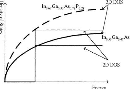
The uniformity of carrier distribution inside the MQW structures is determined by the injection of dominant carrier and the ability to capture carriers in each QW. The carrier distribution will be more concentrated if the QW near the dominant carrier side (n- or p-cladding side) is more able to confine carriers. On the other hand, the carrier distribution will be more uniform if the QW is more incapable of capturing carriers. From section 2. 1 ,theability for the QW to capture carriers is proportional to the 2D density of state. The relation between 3D unconfined DOS and the step-like 2D DOS ofQW are illustrated in Fig. 1. The 2D and 3D DOS's approach the same value at the energy equal to the QW transition energy. Although the valence hand DOS is not perfctly parabolic. the schematic likes Fig. I could he drawn to explain qualitatively: For example. Iflnc3G,it7AS grown lattice-matched to InP substrate, the effective masses of electron and hole are smaller than In)67Ga33As072P028 on lattice-matched lnP substrate. Since effective mass indicates the curvature of 3D DOS ofbulk material, 3D DOS of In53Ga47AS is smaller than 1n67Ga33As072P028 under the same quantized energy, which can be adjusted with QW well thickness. In the same total injection carrier concentration, higher carrier concentration in certain QW produces higher gain for that QW Therefore the uniformity inside nonidentical MQW structure influences laser spectral and electrical, even thermal characteristics. For quaternary material system such as InGaAsI, one can design two kinds of QWs with different corn position but with
same quanUzed energy and same transition energy. Hence one can aJerna the 2D DOS with changing emisiQn wavelength. Also. according to other studies. the temperature sensitivity is related not only to lasing wavelength, but also to material composition". Therefore, with carrier distribution
C,, C CP) (1 C,,
. ..
neigy
Fig. 1 Schematic diagram showing the 3D and 2D DOS ofthe two sets of QWs
inside MQW taken into consideration, one may design a long-wavelength laser diode less sensitive to temperature. In order to prove the concept more clearly, in this work two sets of nonidentical MQW structures with diffrent emission wavelength is designed and described as follows.
3. EXPERIMENT
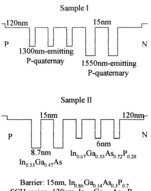
3.1 Nonidentical MQW Design and FabricationLayer structure of designed nonidentical MQW is shown in Fig. 2. Two sets of MQWs, ônm In67Ga33As072P028 triple QWs (designed approximately for lasing wavelength X1 .3im) and 8.7nm ln53Ga47As double QWs (designed approximately for X=l .55.tm), form the basic components of the nonidentical MQW structure. Sample A has the Ifl()53GJ47A5 double QWs near the p-cladding layer. Sample B has the QWs arranged in an opposite sequence. The
QWs are bounded by 1Snm lri086Ga,4As03P07 barrier and the SCH region is l2Onm wiTh the same component as barrier.
Detailed calculations of the emission spectra using Luttingcr-Kohn method, '' showthat the transition energies of the
8.7nm In53Ga47As double QWs are 1 .
54im,1 .46tm, and l A8tm. The transition energies of the 6nm.
1n067Ga033 As072P028
DOS
0
In67Ga33As077P028 triple QWs are 1.3Ojtm and I .24tm.
The nonidentical MQW structures are grown on InP substrate with lattice-matched condition by metal-organic chemical vapor deposition (MO(VD) method. The grown nonidentica! MQW structures are then used to fabricate ridge-waveguide laser diodes (LDs) by standard processing procedures. The ridge ridge-waveguide was created by the technique of electron cyclotron resonance-reactive ion etch (ECR- RIE). The etching was stopped at I OOnm above the SCH layer.
The devices are about 5OOtm long.
Sample I —l2Onm
l5nm
_____
lnnnl 11
p
LiLi
Li H H N
l300nrn-emitting [J
J
P-quaternay 1550nm-ernitting P-quatemaiy Sample II—i_____
l5nm120mm-I
fl nnri
PH
ii U U U
NLi
Li
8.7nm In07Ga33As072P028In0 53Ga0 47As
Barrier: l5nm, In, 86Ga 14As0 3P0 SCM region: l2Onm, Ii86Ga0 14As03P07
Fig. 2 Layer structures of nonidentical MQW for Sample I and Sample H.
3.2 Device Characteristics
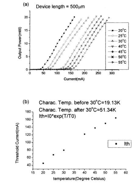
Optical characteristics such as lasing spectra and light-output power relations under temperature varying from 20°C to 55°Care measured on fabricated devices. The L-I curves are measured in pulsed operation with 0.5%dutycycle. More
than 10 laser diodes of each well sequence had been measured and demonstrated similar behavior. The results are shown in Fig. 3(a). Also the threshold currents under dlfferent temperatures are plotted in Fig. 3(b). In Fig. 3kb) one characteristic temperature can not be derived due to the imperfect curve fitting between 3OC and 40°C. The characteristic temperature below 30°C is I 9. 13K, which is poor like the conventional long-wavelength semiconductor laser temperature characteristics. However, for temperature above 30°C, the temperature characteristics improve signiflcantly to 51 .34K. The external quantum efficiency (ii,) underdifferent temperature extracted from Fig. 3(a) is shown in Fig. 4. Under all measured temperatures, t
of
Sample II is higher than that of Sample I. For Sample I, idecreaseswith temperature for the entire meured temperature r!1g. which is si.1Jar to the behavior of
LDs. With increasing temperature, the lasing efficiency of conventional laser diodes fall due to various factors like nonradiative recombination, leakage currents, carrier recombination in SCH layer, etc. However, for sample II, novel
variation of 77dwithtemperature is observed. It first decreases from 41% to 37 % for the temperature varying from 20 °C to 30°C. Then 7dincreasesagain to around 40 % and approximately remains at this value for temperatures above
40°C. The above measurements show that the temperature dependence of threshold current and quantum efficiency could be reduced for certain sequence of nonidentical MQWs.
(a)
Device length = 5QQui.20
j
7 ;/V ft I•1 F1
'
/'7,4i
II J
a a 20°C::
a,,'
'
_1 a/?
I—t--30C
ijlu
a:;
1 /11
' ' 7 f 7
1—v—40°C.-
I"
I •!
I -1' /f'
I ;i ,
7
---%:---- 50°C IT
—÷--- 55°C 0 t U 50 100 150 200 250 300 Current(mA)(b)
Charac. Temp. before 30°C=19.13K180 Charac. Temp. after 30°C=51 .34K
_
16oi lth=IO*exp(T/TO) a a 140j aJ 120
aI
a a•
4u
35 40 45 50S5 do
temperature(DegreeCelsius)Fig.3 (a)L-l relation (b)Threshold currents of Sample I measured in different temperatures.
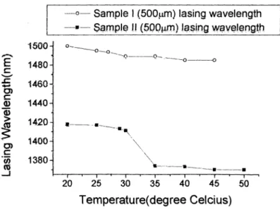
To further realize the novel behavior of temperature characteristics, the variation of lasing wavelength with temperature is also measured. Fig. 5 shows the variation ofthe lasing wavelength with temperature for the two samples. The lasing spectra of Sample I and Sample H under room temperature are about 1 500nm and 1417nm, respectively. The resulting lasing spectra can be regarded as due to the superposition of gain profiles of both I .3tm and I .55jtm QWs. For Sample I, I .55.tm QWs accumulate more carriers than I .3xm QWs, so the gain from 155pm QWs is larger. Thus its lasing mode is mainly contributed from the 87 A QWs. Similarly; the lasing wavelength of Sample II indicates that both the 60 AQWsand the 87 AQWscontribuite gain to the lasing mode. Considering the sequential layout of QWs, the measured lasing spectra imply that more carriers a trapped in QWs near n ..
ide
Fr conventjonal LDs with QWs of the same width. increasing temperature usually results in a red shift of wavelength because of bandgap shrinkage. In this investigation, the LDs with nonidentical QWs behave oppositely. The increase oftemperature causes a blue shift of lasing wavelength for both Sample I and Sample II. In particular, the blue shift of Sample II is quite significant. Its lasing wavelength shifts from 1417nm to 37O nm, nearly 50 nm, for temperature changing from 25°C to 45°C.The reason for the blue shift is because some portion of carriers originally in 1 .55tm QWs move over to 1 3pm QWs when temperature increases. For Sample I, 155pm QWs are near n-side, so carriers move from n-side toward p-side. The change of carriers from I .55p.m QWs to I 3pm QWs is not significant enough, so the lasing wavelength remains near 1500nm,still mainly contributed from the I .55tmQWs. However, such carrier change is already large enough to induce sensitive temperature dependence, causing the threshold current and quantum efficiency to vary
significantly with temperature.
External
quantum efficiency of both facet0.481
, 1'
. 0.4t3
0.44,
0.42,
I
c
0.401 0 38t
0.3C
\
temperature(DegreeCelsius)Fig.4 External quantum efficiency of Sample I under temperature from 20°C to 55°C
I —o— Sample I (5OQum) lasing wavelength
—I—-$amp .1.1 (5QQ1g1)) Jasng wave!gTh
1500
# 1480
Q*—Q
- 1460
C)1
ä3 1440.
1420)
1400 C .3 1380 co s..-. .__.J '1,J',T'
20 25 30 35 40 45 50Temperature(degree
Celcius)
Fig.5variationoflasing wavelengths vs. temperature for Sample I and Sample II.
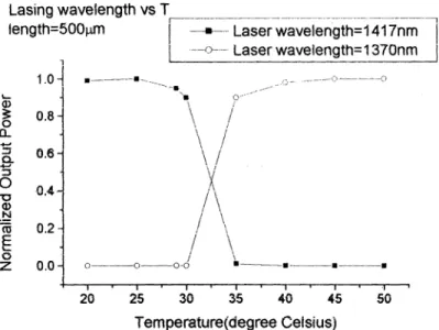
The abrupt changes in characteristic temperature and external quantum efficiency represent transition of lasing state. Shown in Fig. 6 s the output power at 1417 nm and 1370 nm vs. temperature. This figure shows in normalized
output power for individual lasing wavelength. The lasing wavelength changes abruptly from 1417nm at temperature of 3OUC to 1370nm at temperature higher than 35°C. A 47nm lasing wavelength switch is controlled by temperature variation of 5°C. And the output power transfers totally within 10°C range, from 30°C to 40°C. The abrupt lasing wavelength change results from gain competition between 8. 7nrn 1n<53Ga47As double QWs and the 6nm
In67Ga33AsQ72P()28 triple QWs. Lasingwavelength vs T Iength=500pm
[_._Laserwaveiength=i417nm
L •-—°— Laserwavelengtfl=1370nm1.o
0 0.81\ /
:
I.-
0.6\ I
I
Temperature(degree Celsius)Fig.6 Measured lasing wavelength vs. temperature of Sample II LDs
4. DISCUSSION
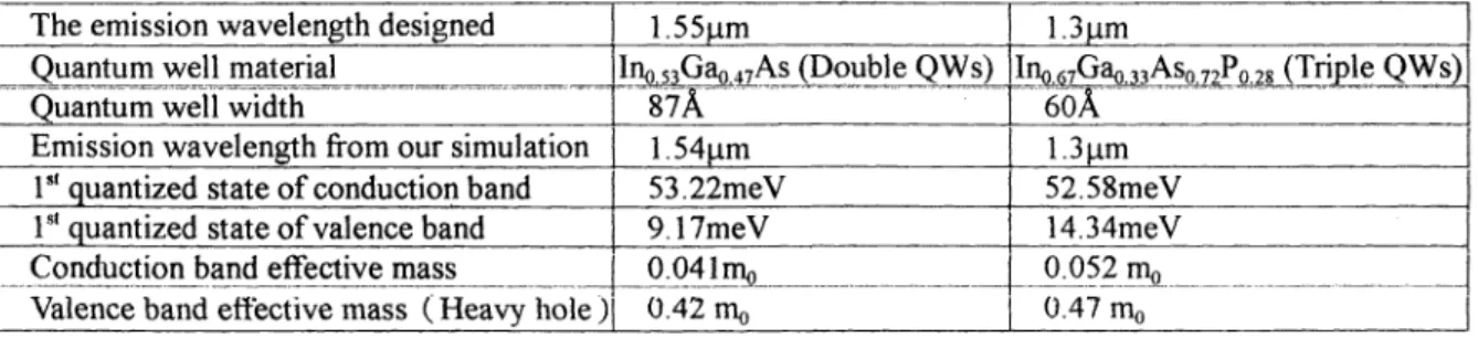
Table I shows the calculation result of n1 transition energy and effective mass of the two sets of MQWs used in Sample A. Note that the QW corresponding to longest emission wavelength always has the highest gain under the same carrier density in each well. Therefore the QW with shorter emission wavelength needs more carrier concentration to
obtain enough gain in order to achieve threshold condition. Fig. 5shows
the lasing wavelength as a result of
superposition of nonklentical MQW gain spectra. From previous researches, it was shown that this MQW structure isdominated by electron due to the long SCH region. As a result, more carriers accumulate in the .QWs near the n-cladding layer, which correspond to the wavelength of I .3tm QWs. Consequently the gain spectrum of each set of QWs is ear1y the sa!Tie 11 the laser diodesQScJJJateat waveleiigths between I ..3urn and J55m. As a rn t of facts
the lasing wavelength is closer to 1.55.tm because the I .55.tmQWs need a lower gain to achieve lasing condition.
When temperature increases, the nonuniformity of carrier distributing inside nonidentical MQW changes, possibly due to more scattering event experienced by carriers. In addition, this change causes the lasing wavelength to shift toward l.3i.tm QWs. Also for the nonidentical MQW a slight change in carrier concentration in certain QWs may change the total gain spectrum abruptly. Therefore the competition for achieving threshold gain between 1 .3.tm and
I .55.tm QWs is dominated by I .3#.tm QW when temperature increases.
When temperature increases, the change of lasing wavelength from 14 17 nm to 1370 nm indicates that the QWs of I .3 m gets more carriers than 1 .55 tm QWs. The reason for carriers in 1 3pm QWs increasing with temperature is explained as follows. When temperature increases, more carriers occupy larger energy states according to Fermi-Dirac distribution, so they can be more possibly captured by 1 3pm QWs than by I .55.tmQWs. Thus the gain contributed
Table I The n= 1 transition energy and effective mass of electron and heavy hole of the two sets of QWs
The emission wavelength designed I 55jim j
I
.3jtmQuantum well width 87A 60A
Emission wavelength from our simulation I .54tm 1 .3tm
' quantized state ofconduction band 53.22meV 5258meV
st quantizedstate ofvalence band 9. 17meV 14.34meV
Valence band effective mass (Heavy
hole ) (3.42 ni
__9____
0.47 m
from I .3.tm QWs increases, resulting in the blue shifi of lasing wavelength. In addition, the nonuniform carrier distribution favoring QWs near n-side, which are 1 3pm QWs for Sample II, causes the blue shift of Sample II to be very significant.
According to the less temperature-sensitive nature of I .3im QW, the temperature sensitivity of laser diode is reduced. Based on the novel discovery long-wavelength laser diodes can be designed by using different QW with different temperature sensitivity inside active region, without change in lasing wavelength.
5.
CONCLUSIONUsing nonidentical MQWs structure, temperature sensitivity of long-wavelength semiconductor lasers can be efficiently reduced. A characteristic temperature increase from 19.13K to 51.34K with temperature change from 30°C to 40°C is observed. Also the lasing wavelength within this temperature change is abrupt, implying change in nonuniform carrier distribution. With the less temperature-sensitive QW located in the proper location, significant improvement on temperature characteristics ofsemiconductor lasers is possible.
ACKNOWLEDGEMENTS
The authors acknowledge the support from National Science Council, ROC under the contract NSC89-21 12-M-002-076 and NSC89-22 l5-E-002-059.
REFERENCES
1 . H. Ishikawa and I. Suemune, "Analysis of temperature dependent optical gain of strained quantum well taking
account ofcarriers in the SCH layer," IEEE Photo,,. Technol. Leit. ,vol.6, pp. 344—347, 1994.
2. C. E. Zah, R. Bhat, B. N. Phatak, F. Favire, W. Lin, M. C. Wang, N. C. Andreadaskis, D. M. Huang, M. A. Koza, T. P. Lee, Z. Wang, D. Darby, D. Flanders, and J. J. Hsieh, "High performance uncooled I .3 Din A1InQa1 As/inP strained layer quantum well lasers for subscriber loop applications," IEEE J. Quantum Electron., vol. 30, pp. 511-522, 1994.
I
K. Nakahara, M. Kondow, T. Kitatani, M ..C.Larson, and K. Uomi, "1 .3-ftm Continuous-Wave Lasing Operation in GainNAs Quantum-Well Lasers," IEEE Photo;,. Technol. Let!., vol. 10, pp. 487-488. 1998.4. N. Tessler and G. Eisenstein, "On carrier injection and gain dynamics in quantum well lasers", IEEE J. Quantum Electron., vol. 29, pp.1586-1595, 1993.
5. N. Tesslerand U Eisenstein, "Distributed nature of quantum well lasers," App!. 1'/zys. Let!. ,vol. 63. pp. 10-12,
1993.
6. B.R. Wu, C. F. Lin, L. W Laih, and T. T. Shih, "Extremely Broadband InGaAsP/InP Superiuminescent Diodes," JEEE1ec:ron. Leit. 36, pp. 2093-2095, 2000,
Nonuniform Carrier Distribution," SPIE Proceedings, Vol. 4283 (Physics and Simulation of Optoelectronic
Devices IX), pp. 659-669, 200 I
8. C. F. Lin, B. R. Wu, L. W. Laih, and T. T. Shih, "Sequence Influence ofNonidenticai InGaAsP Quantum Wells on Broadband Characteristics of Semiconductor Optical Amplifiers! Superlumiraescerit Diodes," Opt. Let!. 26, pp.
lO99llOl,
20019. M. Aam and M. Lundstrom, "Simple analysis of carrier transport and buildup in separate confinement
heterostmcture quantum well lasers". JEEEPhoton Technol. Lett. vol. 6. pp. 141 8-l420 1994.
10. D. Tauber and J. E. Bowers. "Dynamics ofwide bandwidth semiconductor lasers," from High SpeedDiode Lasers, Editor: S. A. Gurevich, pp. 1-40, World Scientific, Singapore, 1998.
I I . K. Otsubo, H. Shoji, T. Kusunoki, T. Suzuki, T. Uchida, Y. Nishijima, K. Nakajima, and H. Ishikawa,
"Long-Wavelength Strained Quantum-Well Lasers Oscillating up to 2IOUC on InGaAs Ternary Substrates," IEiE
Photoni. Technol. Len., Vol. 10, pp. 1073-1075, 1998
12. J. M. Luttinger and W Kohri, "Motion of electrons arid holes in perturbed periodic fields," Phys. Rei 97, pp. 869-883 1955.