Electrical characterisation of the insulating property
of Ta,O, in AI-Ta205-Si02-Si capacitors by
a
low-frequency
C / V
technique
J.-G. HWU S.-T. Lin
Indexing terms: Metal-oxide-semiconductor structures
Abstract: The measurement of equivalent low- frequency capacitance is used as an efficient method to monitor the insulating properties of
Ta,O, in Al-Ta,O,-Si0,-Si (MTOS) structures.
It is found however, that MTOS devices having normal high-frequency C / V characteristics can have significantly different behaviour at low fre- quencies. A technique is proposed in this work that enables the quality of the Ta,O, preparation to be. determined. Examples showing the impor- tance of the measurement of the equivalent low- frequency capacitance are also given.
1 Introduction
Tantalum oxide (Ta,O,) is useful as a capacitor material in some memory applications because of its high dielec- tric constant ( 2 G 2 5 ) [I]. Generally, it can be prepared by direct sputtering [24], thermal oxidation of evaporated Ta CS-71, anodisation [SI or chemical vapour deposition
[9]. Since the insulating property of Ta,O, is the most important parameter in Ta,O,-based devices, almost all workers have examined Ta,O, films by measuring the I / V curve [ l , 4, 71 or the high-frequency C / V [2, 3, 5, 61
characteristics of their devices. It is interesting to note that although the conventional quasistatic C / V technique is essential in examining the interface property between an insulating layer and the Si substrate [lo], it has not been successfully applied to any Ta,O,-based device in the literature. This is mainly because the conduction current of Ta,O, is comparable to the displacement current for most gate voltages [7].
In this work, we analyse the quasistatic C / V curves of
AI-Ta,O,-SO,-Si (MTOS) capacitors because they can
show much information about the insulating property of
Ta,O,
.
Note that the low-frequency capacitanceobtained by the quasistatic C / V technique is an equiva-
lent capacitance, i.e. CLFI,,,, because it contains both the displacement and conduction currents. The effect of the conduction current in Ta,O, on the CL,(,,, of MTOS structures is basically different from the effect of leakage current observed in MOS structures [ll]. A qualitative explanation of this is given below.
Both sputtered and thermal Ta,O, are investigated. The prepared MTOS capacitors all show quite good
Paper 7 4 7 3 6 (E3), first received 2nd October 1989 and in revised form
Zlst February 1990
The authors are with the Department of Electncal Engineering, Nation- al Taiwan University, Taipei, Taiwan, Republic of China
390
high-frequency C / V curves from which one can deter- mine the quantities of the effective fixed charges. However, when the low-frequency C / V characteristics are examined for these samples, one can clearly observe dif- ferences in C,,,,, between them. Since CL,(,,, is sensitive to the insulating property of Ta,O, one can deduce the quality of the Ta,O, from a comparison between CL,(,,, and the high-frequency capacitance C,,
.
From the experimental observations, it is found that, when a sputtered Ta,O, device receives a postmetallisa- tion anneal at 300°C in N,, the insulating property of Ta,O, becomes poor, although the positive fixed charge is significantly reduced. Interestingly, it is also observed that, for a thermal Ta,O, device, the H, anneal at 450°C reduces the number of interface trap states significantly, but does not give any improvement in the insulating pro- perty of Ta,O,, i.e. the Ta,O, becomes leaky after H, annealing. The reduction of the numbering interface trap states after H, annealing is consistent with that observed by Seki in sputtered Ta,O, films, based on the high- frequency C / V technique [3]. However, the change in the insulating property of Ta,O, as a result of the H, anneal,
as observed in this work, is also important in the study. In addition, since the oxidation condition is important to thermal Ta,O, , the dependence of CLFley, on oxidation time is also examined. It is found that C,,(,,, is indeed sensitive to the oxidation time and an optimal oxidation time can therefore be determined from the observed CL,>,,), behaviour. Finally, we use the recently reported radiation-then-anneal method [ 121 to improve the per- formance of MTOS devices. Briefly, when an MOS capa- citor receives repeated radiation-then-anneal treatments, its radiation resistance is much improved. In this work, we find that the fixed charges, the interface trap states and the insulating property of Ta,O, are all improved by this method. A possible explanation is also given.
2 Experiment
p-type and n-type silicon wafers with (lW)-orientation were used as the substrates of MTOS capacitors. After standard cleaning procedures, these wafers were dry- oxidised at 900°C to various oxide thicknesses. Then, two kinds of Ta,O, film were formed on SiO,/Si. One is reac- tively sputtered Ta,O, , obtained under a partial pressure ratio of Ar/O, = 4/1, the other is thermal Ta,O,, made by oxidation of an electron-beam-deposited Ta film under O,/N, at a flow rate ratio of 6/5 at 540°C. Further, aluminum was thermally evaporated on to the samples through metal masks to form contact electrodes. The area of the device discussed in this work was defined by
the area of the aluminum contact electrode. On the back- side of the samples, aluminum was also evaporated, after the oxide was etched away. Note that the thicknesses of Ta,O, were measured by ellipsometry. The surface topography and the thickness uniformity of Ta,O, are not discussed in this work.
Fig. la shows the high-frequency (1 MHz) capacitance
C,, plotted against the gate voltage V, of three MTOS
9 0 o i 1510A 0 5 t -9 - 6 -3 0 3 6 g a t e voltage V , V b G
Fig. 1 Change in capacitunce characteristics caused b y change in
dV,/dt f o r M T O S (n) capacitors
a High-frequency capacitance C,, against gate voltage V, curves of three capa- citors with silicon oxide thicknesses d of430 (SN-1). 900 (SN-2) and 1510 (SN-3)
A and a common tantalum oxide thzkkness d,, of 350 A The Ta,O, IS prepared by direct sputtenng
b C,, and equivalent low-frequency capacitance C against V, curves of a
capacitor with a d,, of 350 A and a d,, of 430 A ( S N - I T Id V,/di 1 = 0.02 VIS
Hold time = 10 s
(n) capacitors, measured using an H P 4275A. The Ta,O, , having a tantalum oxide thickness d,, of 350
A,
was pre- pared by direct sputtering. The thicknesses of silicon oxides d,, for samples SN-1, SN-2 and SN-3, were 430, 900, and lSlOA, respectively. Note that none of these samples received a postmetallisation anneal. The capa- citors seem quite good for these C,,, curves because their hysteresis loops are insignificant and are clockwise in direction. The clockwise hysteresis phenomenon for MTOS (n) capacitors is mainly the result of the trapping of holes at the Si0,jSi interface, but not the leakage current through Ta,O,[SI.
Therefore, not much infor- mation about the insulating property of Ta,O, can be determined from these curves. However, when the con- ventional quasistatic C / V technique is performed on the sample SN-1 using an H P 4140B with a sweep rateIEE PROCEEDINGS, Vol. 137, Pt. G , N o . 5 , OCTOBER 1990
I
dV,/dtI
of 0.02 V/s and a hold time of ten seconds,abnormal capacitance behaviour appears. As can be seen
from the C / V curves in Fig. lb, CLF(eq) is larger than C H F for almost the whole range of V, and there is a split between the curves obtained under forward and back- ward sweeps.
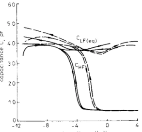
Similarly, an MTOS (p) capacitor prepared under the same conditions as mentioned in Fig. 1 was also exam- ined. Fig. 2a shows the C / V curves of an MTOS (p) capa-
5 0
r
0 . I - A I 4 12 10 - 8 6 - 4 -2 0 a 4 5 - L L a 4 0 - V 3 5 L-
0 3 0 L I251
201
14 -12 -10 - 8 - 6 - 6 2 0 g a t e voltage Vc. v bFig. 2 Dependence of cupucitance characteristics on dVJdt for MTOS ( p ) capacitor
LI C and C,,,,,, against V, curves of a capacitor with a d,, of 266 A and a d,, of 270 r ( S P - I ) The Ta,O, is prepared by direct sputtering
I dV,/di 1 = 0.02 V/s Hold time = 10 s
b Sweep rate dependence of C,,,,,, curvcs lor the same sample
~~~~ 1 dV,/di 1 = 0 01 V/s
_____ 1 dV,/di 1 = 0 02 V/s
~~ 1 dV,/dr 1 = 0.04 Vis
citor, i.e. SP-1, with a d,, of 266
A
and a d,, of 270A.
It is clear that the CL,(,,, behaviour is independent of the sub- strate type. However, when the sweep rate varies, the C,,,,,, behaviour changes, as can be seen from Fig. 2b, the splitting between the CL,(,,, curves obtained under forward and backward sweeps decreases as the sweep rate increases.3 Discussion and examples
3.1 Equivalent low-frequency CjV behaviour Generally, the CL,(,,, obtained by the quasistatic C / V technique is obtained by dividing the measured current I
by dV,/dt. The measured current is purely the displace- ment current I, for an ideal capacitor, but may consist of conduction current I, when the sample is leaky [l 13. In this work, there are two layers, i.e. Ta,O, and SiO,, in an MTOS capacitor. The SiO, layer can be regarded as an ideal insulator with respect to the Ta,O, layer. The charges moving within the Ta,O, layer due to the elec- tric field introduce an I, component to the total mea- sured l and are accumulated somewhere in the Ta,O,
.
Since the growth of pinholes is unstable, the conduction
mechanism within the Ta,O, is complicated [4, 131, and
is basically different from that for the leakage current that flows through a device similar to an MOS capacitor
[ll]. Fig. 3 shows the simplified equivalent circuit of an
I D
-
44
csx c sFig. 3 Simplified equivalent circuit for an M T O S capacitor with a T a , O , leakage resistance R,,
C,,, C , and C, are the capacitances ofTa,O,, SiO, and SI, respectively. I , and
I , are the conduction current and the displacement current through Ta,O,, respectively, during low-frequency C / V measurement. Q 1s the effective trapped charge within the Ta,O,. I is the total measured current
I , + 1,
cLf,m = dv,/dt
I = I , + I ,
MTOS capacitor. C,, , C,, , and C, are the capacitances of
Ta,O, , SiO, and silicon substrate, respectively. R,, rep- resents the leakage resistance of Ta,O, , which is a com- plicated function of V, , d V , / d t and the charges trapped in the Ta,O, layer Q. When I, is important, I can be written as
I = I ,
+
I , (1)Then, CL,(,,, can be expressed as
U
-
dt
When V, sweeps from negative to positive, i.e. dV,/dt > 0, I , is positive over the whole V, range, but I , may change from negative to positive during a sweep. There- fore, the contribution of I, to CL,(,,, is first subtracted, when the directions of I, and I, are opposite, and is then added when the directions are the same. Similarly, when V, sweeps from positive to negative, i.e. dV,/dt < 0, the same effect on the contribution of I, to CL,(,,, occurs as is described above. Near the positive V, range, I, is nega- tive, but I, is positive so CL,(,,, is reduced. While near the negative V, range, I, and I, are both negative so CLPfeq) is increased. It is clear from the above discussion that I, accounts for the splitting of the CL,(,,, curves, and the dependency of CL,(,,, on dV,/dt, as observed in Fig. 2b, is explainable.
It is also noted that the condition when I, changes
sign during forward or backward sweeping depends on
the electric field that the Ta,O, layer has sustained. When the trapped negative charge in the Ta,O, is large, it is possible that the electric field in the Ta,O, is still positive at a certain negative V, during forward sweep-
392
ing. Under such a circumstance, I, and I, are both posi- tive and contribute a higher value of CLF(eq, than C,, over the whole V, range. Similarly, the same behaviour can also occur during backward sweeping. Therefore, the higher value of CLF(eq, compared with C,, observed in
MTOS capacitors is basically different from that observed in an MOS capacitor. However, it is sufficient to note that the measurement of CLF(eq, can be a useful method by which to examine the insulating property of T a z 0 5 in MTOS structures.
3.2 Effects of postmetallisation annealing in N2 Generally, when an MTOS device receives a postmetalli- sation annealing, its interface trap states and fixed oxide charges can be reduced to an insignificant level. However, there is lack of information about the effect of postmetal- lisation annealing on the insulating property of Ta,O,
.
Fig. 4 shows the C,, and CL,(,,, curves of the MTOS (p)
5 0
i:[
.
I
- 12 - 8 -1, 0 1,
g a t e v o l t a g e VG,V
Fig. 4 C,,, and CLF,eq, against V, curves oJ an M T O S ( p ) capacitor ( S P - I ) before and after postmetallisation annealing in N , at 300"CfOr ten minutes
The Ta,O, is prepared by direct sputtering
d = 266 A
d z = 270 A
~ before annealing ~~~~ after annealing
capacitor with sputtered Ta,O, as discussed in relation to Fig. 2, i.e. SP-1, before and after receiving a postmetal- lisation annealing in N, at 300°C for 10 minutes. It is clear that the insulating property of Ta,O, becomes poor after annealing since CL,(,,, after annealing is larger than that before annealing. The shift of C,, as a result of annealing accounts for the reduction of the effective posi- tive oxide fixed charge. Unfortunately, this anneal is insufficient to eliminate the slow trapping states since the counterclockwise hysteresis loop is still distinguishable after annealing. So, it can be noted from the above dis- cussion that the measurement of
c,,(,,,,
in addition to C,, , is important when analysing an MTOS device after it has been subjected to a thermal annealing. It is noted that the possible chemical reaction during annealing, between the aluminium metal electrode and the Ta,O, ,is beyond discussion in this work. However, since the maximum values of C,, before and after annealing are almost equal, the change in the effective area due to this reaction is negligible.
3.3 Effects of postoxidation annealing in H,
T o show the effect of postoxidation annealing in
H,
on the insulating property of Ta,O, , two MTOS (p) capa- citors, i.e. TP-1 and TP-2, were compared. The Ta,O,layers in these samples were prepared by thermal oxida- tion at 540°C for 90 minutes simultaneously. The final thicknesses of Ta,O, and SiO, layers were 650 8, and
400
A,
respectively. It should be noted that TP-2 received a postoxidation annealing in H, at 450°C for 30 minutes,but TP-1 did not. Their normalised CjV curves are
shown in Fig. 5. Note that the behaviour of CLF(eq) for
--.
/---.
-.
-
-
E 02L-.-#
- 5 - 4 -3 - 2 -1 0 1 1 2 1 g a t e v o l t a g e V G , VFig. 5 Normalised C,, and CLF,oq) against V, curves of two M T O S
(p) capacitors with (TP-2) and without ( T P - I ) postoxidation annealing in
H , at 450°C for 30 minutes
The Ta,O, is prepared by thermal oxidation at 540°C for YO minutes
d,- = 650 A
d,, = 4M) A
-~ no H, annealing H, annealed
~~ ~~
thermally grown Ta,O, , as shown in Fig. 5, is different from that for sputtered Ta,O, , as shown in Fig. 4. This is mainly due to the radiation damage to the Ta,O, during sputtering. As can be seen from the C,, curves, TP-2 appears to exhibit a steeper behaviour with respect to changing gate voltage than TP-1 in the depletion region and there is no hysteresis phenomenon for either sample. Therefore, the number of slow trap states is negli- gible and the number of interface trap states can be sig-
/
1’
/
/i
10’1 1 0 0 -0 10 20 30 1 0 50 60 70 o x i d a t i o n t l m e minutes Fig. 6 (TP-3) oxidlsed at 540°CThe space S between the two measurement probes IS 2 mm
Reslstance R agalnst oxzdatlon time of an M T O S ( p ) capacitor
nificantly reduced by H, annealing. However, as can be seen from the CL,(,,, curves, TP-2 appears to have a larger value for and a larger split in CL,(,,, than TP-1 so the insulating property of Ta,O, becomes poor after H, annealing. It seems quite clear from Figs. 4 and 5 that this property of Ta,O, is very sensitive to a thermal treatment.
3.4 Optimal oxidation time for thermal Ta, 0, For thermal oxidation of a Ta film at a certain tem- perature, the oxidation time is one of the important parameters. However, it is rather difficult to accurately control the oxidation time, since it depends on the thick- ness of Ta film and the oxidation conditions. In this work, we propose that the insulating property of Ta,O, during thermal oxidation be detected by measuring and plotting surface resistance R and current I against V, or CL,(,,, against V,
.
10.‘r
10 - 4 - 2 0 a UI
- I 21
-1
,
- 2 lo - 4 n q o - ’ or
b - L -2 0 2 1 C g a t e v o l t a g e VG, V Fig. 7(thermal T a , O , ) oxidised at 540”Cfor different lengths oftime
d ~ ~ = 4 0 0 A ; I d V , / d t I = O . O 2 V / s a 60 minules (TP-4-11 h 70 minules (TP-4-2) c YO and I IO minutes ~~~ YO minutes (TP-4-3) ~ I10 minutes (TP-4-4)
Current I 11 against V, curves of four M T O S (p) capacitors
393 IEE PROCEEDINGS, Vol. 137, Pt G, No. 5. OCTOBER 1990
L
LL a 1 4 : 1 0w
0 6 1 I-
0 2 / < I 1 I I - 6 - 4 - 2 g a t e voltoge VG, V CFig. 8 Normalised C,, and C,,,,,, against V' curves of three M T O S
(p) capacitors (thermal T a , O , ) oxidised at 540°C for different lengths of time
d,, = 650 A. d,, = 400 A ; I dV,/dr I = 0.02 V/s
0 75 minutes (TP-5-1)
b 90 minutes (TP-5-2)
c 105 minutes (TP-5-31
In the early period of thermal oxidation, most of the Ta film is still conductive so the surface resistance of the sample under test can be easily measured using a multi- meter. Fig. 6 shows R against oxidation time for a
sample, i.e., TP-3, oxidised at 540°C. The thickness of the SiO, layer under the Ta film is 400
A.
The space between the two measurement probes S is 2mm. Note that theprobes touch the sample surface directly without prep- aration of the contact electrode. As expected, the resist- ance increases as the oxidation time increases. When the oxidation time exceeds about 1 h, R is too high to be accurately measured in this way.
If the C,,,,,, technique mentioned above is used in a very leaky sample, the capacitance value is beyond the range of the H P 4140B meter, because of the large current. It is therefore better to make measurements in the current mode rather than the capacitance mode under such a circumstance. Fig. 7 shows the absolute
394 I C 3 0 -
I
---.
- 6 - I - 2 0 i d g a t e v o l t a g e V G , V Fig. 9capacitor (thermal Ta,O,)
U After poslmetallisauon annealing ( W C , N, IO mm)
b After first radiation and anneal treatment
r After second treatment
d Alter third treatment
d,x = 360 A ~~~ irradiated (CO'', 10 kGy)
d,, = 500 A ~ ~ annealed
C,, and C,,,,, against V' curues of an M T O S ( p ) ( T P - 6 )
current 11
I
against V', for four samples, i.e., TP-4-1, TP-4-2, TP-4-3 and TP-4-4, oxidised a t 540°C for 60, 70, 90 and 110 minutes, respectively. The sweep rate isI
dV,/dtI
= 0.02 V/s for each measurement. As can be seen from Fig. 7a, the current is quite large. This is mainly due to the conduction current through the Ta,O,.
Sample TP-4-1 is very conductive, but for sample TP-4-2, as shown in Fig. 76, the displacement current of the Ta,O, is no longer negligible because the conduction current of the Ta,O, decreases. This contributes a smallhysteresis phenomenon to the 111 against V, curves
shown in this figure. When the oxidation time increases to 90 or 110 minutes, as shown in Fig. 7c, the conduction current of Ta,O, decreases further and the displacement current becomes a greater proportion of
I
I1 .
However, the oxidation time of 90 or 110 minutes is still not good enough since the hysteresis phenomena for samples TP-4- 3 and TP-4-4 are both significant.Figs. 8a, b and c show the normalised capacitance C/C,,,,,, against V, for three other samples, i.e. TP-5-1, TP-5-2 and TP-5-3, oxidised at 540°C for 75, 90 and 105 minutes, respectively. Note that the initial thick- ness of the Ta films for these samples are different from those of the films whose characteristics are shown in Fig. 7 and that the optimal oxidation time for the samples of Fig. 8 is different from that for those in Fig. 7. As can be seen from Fig. 8, all the C,, curves are good enough to be distinguished. But, an oxidation time of 90 minutes gives the best CL,(,,, behaviour of the three. A long oxi- dation time may enhance the growth of pinholes and therefore increase the leakage current [4].
3.5 Improvement of the insulating property of Ta,O, by repeated radiation -then -anneal treatments When an MTOS capacitor receives Co60 irradiation to a total dose of 10 kGy, the radiation-induced holes (or
electrons) can be partially trapped in the oxide layers by the hole (or electron) trapping centres. Therefore, the C / V curve after irradiation will shift, because of the change in the effective trapped charge. However, when the irradi- ated MTOS capacitor receives a subsequent anneal in N, at 400°C for ten minutes, the radiation-induced damage can be substantially eliminated. Fig. 9 shows the C / V curves for a thermal MTOS capacitor, i.e. TP-6, before and after such treatments. Fig. 9a shows the C / V curves after postmetallisation annealing (PMA). The C / V curves after the first, second and third radiation and anneal treatments are shown in Figs. 9b, c and d, respectively. There are some important phenomena to observe in these figures. For a clear understanding, the C / V curves after PMA, i.e. the curves in Fig. 9a, and after repeated radiation-then-anneal treatments, i.e. the solid curves in
Fig. 9d, are shown together in Fig. 10. From the C,, curves, it is to be noted that the numbers of effective posi- tive charges in the insulators are significantly reduced after treatments. Furthermore, from the comparisons between the CL,(,,I curves and the C,, curves near the depletion region, the number of interface trap states at the SiO,/Si interface is also reduced. Interestingly, the splitting of the CL,,,,, curves after treatment is smaller than that before treatment. Therefore, the insulating property of Ta,05 is improved by this method. This is
probabily because of the removal of the strain, related to trapping centres in the Ta,O, , which are responsible for its conduction current, by repeated radiation-then-anneal treatments [14].
Finally, the flat-band voltage VFB and the effective fixed charge
Q
,
,
,
against the number of treatments areIEE PROCEEDINGS, Vol. 137, P i . C , No. 5. O C T O B E R 1990
shown in Fig. 11, based on the C / V curves shown in Fig. 9. It is clear that V,, (or Qe,,) decreases gradually after each radiation or each anneal as the number of treat-
loor
0 ' . ' " " " - 6 - A - 2 g a t e v o l t a g e VG, V Fig. 10of Fig. 9 before and after repeated radiation-then-anneal treatments
~-
~~ repeatedly radiation-then-anneal treated
C,, and C,,,,, against V , curves of the M T O S (p) capacitor
postmetallisation annealed (400°C. N,, 10 mtn) 0 I 0 0 1 0 0 1 2 3 a 0 0 0 1 2 3 number of t r e a t m e n t s b Fig. 11
from C,, curves of Fig. 9
U Ellect on Rat-band vollage V,,
h ERect on eKective fixed chargee*,,
after radiation (CO''. 10 kGy)
0 alter anneal (400°C. N,, 10 mm)
Effecfs oJ repeated radiarion-then-anneal freafmenl, derived
ments increases. Therefore, the ‘radiation-hardness’ of MTOS capacitors is also improved by this method.
4 Conclusions
Observation of the equivalent low-frequency capacitance of an MTOS capacitor gives one a method of direct examination of the insulating property of Ta,O,
.
By the use of this technique, a dependence on the process ofpreparation of the Ta,O, is found. The insulating
property of Ta,O, becomes poor when it receives a post metallisation anneal in N, or a postoxidation anneal in
H , . For thermal Ta,O,, the optimal oxidation time is achievable by examination of the condition when the C,,,,,, behaviour is least leaky. Repeated radiation-then- anneal treatments improve the insulating property of
Ta,O, and also reduce the effective positive fixed charge and the concentration of interface trap stages.
5 Acknowledgment
The authors want to thank the National Science Council of the Republic of China for the support of this work under contract No. NSC78-0404-E002-01.
6 References
1 OHTA, K., YAMADA, K., SHIMIZU, K., and TARUI, Y.: ’Quad- ruply self-aligned stacked high-capacitance RAM using Ta,O, high- density VLSI dynamic memory’, IEEE Trans., 1982, ED-29, pp. 368-376
2 ROBERT, S., RYAN, J., and NESBIT, L.: ‘Selective studies of crys- talline Ta,O, films’, J. Electrochem. Soc., 1986, 133, pp. 140-1410
3 SEKI, S., UNAGAMI, T., and TSUJIYAMA, B.: ‘Electrical charac- teristics of tantalum centoxide-silicon dioxidesilicon structures’,
ibid., 1985, 132, pp. 199-202
4 KIMURA, S., NISHIOKA, Y., SHINTANI, A., and MUKAI, K.: ‘Leakage-current increase in amomhous Ta.0. films due to Dinhole growtcduring annealing below &C‘, ibih., i983, 130, pp: 2414- 2418
5 HWU, J.G., JENG, M.J., WANG, W.S., and TU, Y.K.: ‘Clockwise
C-V hysteresis phenomena of metal-tantalum oxide-silicon oxide- silicon (p) capacitors due to leakage current through tantalum oxide’, J. Appl. Phys., 1987, 62, pp. 42774283
6 HWU, J.G., and JENG, M.J.: ‘C-V hysteresis instability in aluminum/tantalum oxide/silicon oxide/silicon capacitors due to postmetallization annealing and CO-60 irradiation’, J. Electrochem.
Soc., 1988,135, pp. 280&2813
7 OEHRLEIN. G.S.: ‘Caoacitance-voltaee mooerties of thin Ta,O.
- . .
-~
films on silicon’, Thin Solid Films, 1988,156, pp. 207-229 8 ANGLE, R.L., and TALLEY, H.E.: ‘Electrical and charge storagecharacteristics of the tantalum oxide-silicon dioxide device’, IEEE
Trans., 1978, ED-25, pp. 1277-1283
9 KAPLAN, E., BALOG, M., and BENTCHKOWSKY, D.F.:
‘Chemical vapor deposition of tantalum pentoxide films for metal- insulator-semiconductor devices’, J. Electrochem. Soc., 1976, 123, pp. 1570-1573
10 MANCHANDA, L., and GURVITCH, M.: ‘Yttrium oxide/silicon dioxide: a new dielectric structure for VLSl/ULSl circuits’, IEEE
Electron Device Lett., 1988,9, pp. 180-182
I I MONDERER, B., and LAKHANI, A.A.: ‘Measurement of the quasi-static C-V curves of an MIS structure in the presence of charge leakage’, Solid-state Electron., 1985, 28, pp. 447451 12 HWU, J.G., and FU, S.L.: ‘Improvement in radiation hardness of
oxide by successive irradiation-then-anneal treatments’, ibid., 1989, 32, pp. 615-620
13 OEHRLEIN, G.S.: ‘Oxidation temperature dependence of the dc electrical conduction characteristics and dielectric strength of thin Ta,O, films on silicon’, J. Appl. Phys., 1986, 59, pp. 1587-1595 14 HWU, J.G., and CHEN, J.T.: ‘Improvement of hotelectron-induced
degradation in MOS capacitors by repeated irradiation-then-anneal treatments’, IEEE Electron Device Left., 1990, 11, pp. 82-84