Modeling of nitrogen profile effects on direct tunneling probability in ultrathin nitrided
oxides
Po-Tsun Liu, Chen-Shuo Huang, D. Y. Lee, P. S. Lim, S. W. Lin, C. C. Chen, H. J. Tao, and Y. J. Mii
Citation: Applied Physics Letters 92, 022112 (2008); doi: 10.1063/1.2835706 View online: http://dx.doi.org/10.1063/1.2835706
View Table of Contents: http://scitation.aip.org/content/aip/journal/apl/92/2?ver=pdfcov Published by the AIP Publishing
Articles you may be interested in
Tunneling current at the interface of silicon and silicon dioxide partly embedded with silicon nanocrystals in metal oxide semiconductor structures
J. Appl. Phys. 101, 024315 (2007); 10.1063/1.2425290
Modeling and characterization of direct tunneling hole current through ultrathin gate oxide in p-metal–oxide–semiconductor field-effect transistors
Appl. Phys. Lett. 78, 4034 (2001); 10.1063/1.1379786
Tunneling through ultrathin SiO 2 gate oxides from microscopic models J. Appl. Phys. 89, 348 (2001); 10.1063/1.1330764
Analytic model of direct tunnel current through ultrathin gate oxides J. Appl. Phys. 87, 3000 (2000); 10.1063/1.372290
Tunneling currents through ultrathin oxide/nitride dual layer gate dielectrics for advanced microelectronic devices J. Appl. Phys. 83, 2327 (1998); 10.1063/1.366976
This article is copyrighted as indicated in the article. Reuse of AIP content is subject to the terms at: http://scitation.aip.org/termsconditions. Downloaded to IP: 140.113.38.11 On: Wed, 30 Apr 2014 23:17:49
Modeling of nitrogen profile effects on direct tunneling probability
in ultrathin nitrided oxides
Po-Tsun Liua兲
Department of Photonics and Display Institute, National Chiao Tung University, 1001 Ta-Hsueh Rd., HsinChu 300, Taiwan, Republic of China
Chen-Shuo Huang
Institute of Electro-Optical Engineering, National Chiao Tung University, 1001 Ta-Hsueh Rd., HsinChu 30010, Taiwan, Republic of China
D. Y. Lee, P. S. Lim, S. W. Lin, C. C. Chen, H. J. Tao, and Y. J. Mii
R&D, Taiwan Semiconductor Manufacturing Company, No. 8, Li-Hsin Rd. 6, Hsinchu Science Park, Hsinchu 300-77, Taiwan, Republic of China
共Received 30 October 2007; accepted 21 November 2007; published online 18 January 2008兲 The dependence of the gate tunneling current共Jg兲 on nitrogen profile 共N profile兲 within an ultrathin silicon oxynitride film is reported. It was found that gate tunneling current is dependent on N profile, even with equal oxide thickness and nitrogen dosage. Gate tunneling current increased with steeper N profile, and it had higher sensitivity for p-type metal-oxide-semiconductor field-effect transistor 共MOSFET兲 than n-type MOSFET. A direct tunneling model based on Wentzel-Kramers-Brillouin approximation has been proposed. The model described the influence of N profiles on gate tunneling current through local change of dielectric constant, band bending, and effective mass. Also, it reasonably explained the different Jgsensitivity in n-/p-MOSFETs, a phenomenon that has not been addressed in earlier publications. © 2008 American Institute of Physics.关DOI:10.1063/1.2835706兴
Device downscaling was initially achieved by simply re-ducing the physical thickness of SiO2. The downscaling of device thickness, however, causes gate tunneling current to increase exponentially and boron penetration issue to emerge. These issues pose great challenges to the continua-tion of the device downscaling. To overcome these issues, silicon oxinitride 共SiON兲 was adopted extensively, and downscaling continues with the scaling of physical thickness and the increasing nitrogen concentration within SiON film. Nevertheless, excessive nitrogen concentration poses several other issues on device reliability, such as severe threshold voltage shift, lower mobility, and degraded negative bias temperature instability.1 Therefore, the control of nitrogen profile 共N profile兲 in the ultrathin SiON becomes specially critical.2 Successful N-profile engineering will definitely al-leviate these issues mentioned, if not solve them completely.3 Numerous publications have been reported to suppress the gate tunneling current through the incorporation of nitro-gen into the SiON film. For the same effective oxide thick-ness 共EOT兲, a lower tunneling current is possible to be achieved by increasing the nitrogen concentration. Numerous models also have been proposed to explain the dependence of nitrogen dosage on gate tunneling current.4–6 In these models, uniformly distributed N profile is normally assumed. Little attention has been paid to study the influence of N profile on the gate tunneling current. Typically, the nitrogen profile is intentionally engineered to optimize the benefits in both device and reliability. In this work, the effects of differ-ent N profiles within an ultrathin SiON on the evdiffer-entual gate tunneling current have been investigated. A model based on Wentzel-Kramers-Brillouin共WKB兲 approximation7has been proposed to explain how the steeper N profile contributes to
the high gate tunneling current 共Jg兲. In addition, it well ex-plains the evolution of tunneling current by considering the local variations in dielectric constant, band profile, and ef-fective mass.
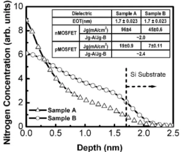
To investigate the impact of N profile on gate tunneling current, two kinds of SiON samples 共“sample A” and “sample B”兲 with different N profiles were fabricated. Sample A had a steeper N profile than sample B, as illus-trated in Fig. 1. The N profile was measured using high-resolution angle-resolved x-ray photoelectron spectroscopy 共XPS兲. Both thickness and N dosage were kept equal for the two kinds of samples. The corresponding electrical data in terms of EOT, inversion gate tunneling current共Jg兲, and Jg
a兲Electronic mail: [email protected].
FIG. 1. Comparison of nitrogen depth profile共N profile兲 and gate tunneling current共Jg兲 for two kinds of SiON films with similar thicknesses and
nitro-gen concentrations. The N profile was measured using high resolution angle-resolved XPS. Sample A共open triangle兲 has a steeper N profile than that of sample B共open circle兲. Gate tunneling-current density was measured at Vg=⫾1 V, with other terminals being connected to ground potentials.
APPLIED PHYSICS LETTERS 92, 022112共2008兲
0003-6951/2008/92共2兲/022112/3/$23.00 92, 022112-1 © 2008 American Institute of Physics
This article is copyrighted as indicated in the article. Reuse of AIP content is subject to the terms at: http://scitation.aip.org/termsconditions. Downloaded to IP: 140.113.38.11 On: Wed, 30 Apr 2014 23:17:49
ratio 共defined as Jg-A/Jg-B兲 are summarized in the inset of Fig.1. Two key observations were made from these experi-mental data. Firstly, sample A exhibits a higher Jgthan that of sample B, for both n- and p-MOSFETs. Secondly, Jgratio is higher in p-MOSFET than that in n-MOSFET, indicating that p-MOSFET has a higher sensitivity to Jg with the change of N profile. Based on the change of tunneling prob-ability, a model arising from the localized band bending is proposed to explain these experimental data. In the model, WKB approximation is adopted to calculate the change of tunneling probability under various biasing conditions.7The tunneling probability共Tt兲 could be expressed by
Tt= exp
冋
− 2冕
0Tphy
冑
2m*共x兲ប 关⌽SiON共x兲 − E兴dx
册
, 共1兲 where Tt⬅tunneling probability, Tphy⬅physical thickness of dielectric, ⌽SiON⬅SiON/Si potential barrier, and m* ⬅carrier’s effective mass and x⬅distance into SiON, deter-mined from the interface of poly Si and SiON.Two parameters ⌽SiON共x兲 and m*共x兲, under different gate biases, must be extracted first to solve Tt. Also, several assumptions were made to simplify the model. Firstly, the nitrogen concentration is assumed to vary linearly within the bulk of SiON. Secondly, the bulk of SiON film is assumed to consist of n pieces of very thin SiON strips with uniformly distributed nitrogen in the every strip. Thirdly, the energy barrier height共兲, dielectric constant 共兲, and effective tun-neling mass共m*兲 for SiON are assumed to vary linearly with nitrogen dosage between oxide material constants and those for nitride, as reference to Muraoka et al.6and Kraus et al.8 It follows that the various input parameters could be simpli-fied as follows: N共x兲 = a1x + a2, 共2兲 共N兲 =ox+共SiN−ox兲 N NSiN , 共3兲
共N兲 = ox+共SiN−ox兲 N NSiN
, and 共4兲
m*共N兲 = mox* +共mSiN* − mox*兲 N NSiN
, 共5兲
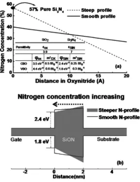
where a1and a2are constants, and we can obtain a variety of linear N profile shapes by modifying those values. The N and NSiNare nitrogen concentrations at. % in the oxynitride film and the pure nitride film, respectively. The other used con-stants are summarized in the inset of Fig. 2. Substituting these parameters 关共x兲, 共x兲, and m*共x兲兴 into the main ex-pression in Eq.共1兲, we could simulate the tunneling probabil-ity through the different potential barriers. Figure2共b兲shows the simulated band diagram under a gate bias共Vg兲 of 0 V.
For Vg⫽0, Poisson’s equation shall be adopted to de-scribe the nonhomogeneous change of dielectric constant within SiON:
d dx
冋
共x兲dVSiON共x兲
dx
册
== 0, 共6兲where VSiON共x兲 andare representing the potential and free charge density within SiON, respectively. Solving for Pois-son’s equation, the band diagram of SiON film with different N profiles can be simulated共not shown兲. Therefore, the cor-responding tunneling probability for n-MOSFET under Vg ⬎0 V and for p-MOSFET under Vg⬍0 V can be simulated. To examine our model, two kinds of SiON samples with different N profiles are considered, as depicted in Fig.2共a兲. Both samples have equal nitrogen concentrations and film thicknesses. Under zero bias 共i.e., Vg= 0 V兲, the simulated energy band diagrams are shown in Fig. 2共b兲. The SiON sample with a steeper N profile exhibits a steeper conduction band共CB兲 and valence band 共VB兲 bendings. Take note that
FIG. 2.共a兲 Schematic showing for two kinds of N profiles: the steep vs the smooth profile. The maximum nitrogen was set to be the pure nitride共N = 57%兲. These two scenarios were used as simulation inputs to assess the impact of N profile to Jg. The various constants used in simulations are
listed as the inset.共b兲 Simulation output 共at Vg= 0 V兲 for the corresponding
energy band diagrams shown in共a兲. It is assumed that the depth of distrib-uted nitrogen concentration is kept equal. In the inset of Fig.2共a兲, CB0and VB0are conduction band offset and valence band offset, respectively.
FIG. 3. Tunneling probability共TP兲 for electrons and holes under various biasing conditions. TP was obtained from simulation result by using our proposed model. The tunneling probability ratio 共TP ratio兲 is defined as TPsteep/TPsmooth.
022112-2 Liu et al. Appl. Phys. Lett. 92, 022112共2008兲
This article is copyrighted as indicated in the article. Reuse of AIP content is subject to the terms at: http://scitation.aip.org/termsconditions. Downloaded to IP: 140.113.38.11 On: Wed, 30 Apr 2014 23:17:49
the degree of VB bending is steeper than that of CB. This is attributed to the greater VB offset 共than CB offset兲 differ-ence, comparing SiO2to Si3N4, as shown in the inset of Fig. 2共a兲.
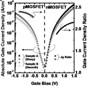
Under nonzero biasing 共i.e., Vg⫽0兲, there will be an additional voltage drops across the silicon oxinitride共VSiON兲. Hence, it is necessary to consider both共x兲 and VSiON共x兲 for constructing the potential barrier, while simulating the en-ergy band diagrams. Considering minority carriers under op-eration mode共at low electric field兲,10the simulated tunneling probability for electrons 共in n-MOSFET兲 under positive bi-asing, and holes共in p MOSFET兲 under negative biasing are plotted in Fig.3. These experimental results are also shown in Fig.4. These I-V curves in Fig.4are the average results of five devices for each kind of samples. The gate current den-sity共Jg兲 ratios of the steep profile to the smooth profile for
n/p-MOSFETs are also presented. The range of gate bias for
measuring Jgratios is just shown between −1.25– −0.5 V for
p-MOSFET and between 0.5 and 1.5 V for n-MOSFET. The
carrier transport mechanism in the bias range can be attrib-uted to the direct tunneling behavior, which is verified by conduction processes fitting.7
According to simulated results, it shows that the sample with steeper N profile exhibits a higher tunneling probability, valid for both n- and p-MOSFETs. This result agrees well with our experimental data in Fig. 4. On the other hand, defining the tunneling probability ratio 共TP ratio兲 as TPsteep/TPsmooth, it is observed that holes共in the p-MOSFET兲 have a higher TP ratio than electrons共in the n-MOSFET兲. In other words, SiON with steeper N profile gives rise to a higher JG increase. This is particularly true for p MOSFET because VB bending is more sensitive to N profile change than CB bending, as predicted by our model.
In summary, we have proposed a model based on WKB to well explain the gate tunneling current through thin SiON film with different N profiles. The change in N profile influ-ences the band shape of SiON film, leading to the change in the tunneling probability. The SiON film with a steeper N profile will exhibit a higher gate tunneling current. Also, the phenomenon is more apparent in p-MOSFET than in
n-MOSFET. The higher sensitivity of VB bending toward N
profile change reasonably explains that p-MOSFET is show-ing a larger current increment than n MOSFET.
The authors would like to acknowledge the financial support of the National Science Council共NSC兲 under Con-tract Nos. NSC 95-2221-E-009-0254-MY2, NSC 96-2221-E-009-130-MY3, and NSC 96-2218-E-009-009 and partial sup-port by MOE ATU Program and MOEA Technology Development for Academia Project No. 94-EC-17-A-07-S1-046.
1N. Kimizuka, K. Yamaguchi, K. Imai, T. Iizuka, C. T. Liu, R. C. Keller, and T. Horiuchi, IEEE Symposium on VLSI Technology, Digest of Tech-nical Papers, 13–15 June 2000, p. 92.
2C.-C. Chen, V. S. Chang, Y. Jin, C.-H. Chen, T.-L. Lee, S.-C. Chen, and M.-S. Liang, IEEE Symposium on VLSI Technology, Digest of Technical Papers, 15–17 June 2004, p. 176.
3M. Terai, K. Watanabe, and S. Fujieda, IEEE Trans. Electron Devices 54, 1658共2007兲.
4H. Yu, Y. T. Hou, M. F. Li, and D. L. Kwong, IEEE Trans. Electron Devices 49, 1158共2002兲.
5M. Togo, K. Watanabe, T. Yamamoto, N. Ikarashi, T. Tatsumi, H. Ono, and T. Mogami, IEEE Trans. Electron Devices 49, 1903共2002兲. 6K. Muraoka, K. Kurihara, N. Yasuda, and H. Satake, J. Appl. Phys. 94,
2038共2003兲.
7S. M. Sze and K. K. Ng, Physics of Semiconductor Devices, 3rd ed. 共Wiley, New York, 2007兲 Vol. 48, p. 227.
8P. A. Kraus, K. Z. Ahmed, C. S. Olsen, and F. Nouri, IEEE Trans. Electron Devices 52, 1141共2005兲.
9J. Robertson, J. Vac. Sci. Technol. B 18, 1785共2000兲.
10Y. C. Yeo, Q. Lu, W. C. Lee, T.-J. King, C. Hu, X. Wang, X. Guo, and T. P. Ma, IEEE Trans. Electron Devices 21, 540共2000兲.
FIG. 4. The gate leakage current density 共Jg兲 for n-MOSFET and
p-MOSFET under various bias conditions. The gate current density 共Jg兲
ratios of the steep profile to the smooth profile for n-/p-MOSFETs were also presented. The carrier transport mechanism in the bias range of Jgratio
can be attributed to the direct tunneling, which is verified by conduction processes fitting共see the Ref.7兲.
022112-3 Liu et al. Appl. Phys. Lett. 92, 022112共2008兲
This article is copyrighted as indicated in the article. Reuse of AIP content is subject to the terms at: http://scitation.aip.org/termsconditions. Downloaded to IP: 140.113.38.11 On: Wed, 30 Apr 2014 23:17:49