國 立 交 通 大 學
電子工程學系電子研究所碩士班
碩 士 論 文
利用多層感測層改善酸鹼離子感測器
飄移特性之研究
The study of improving drift characteristics with
multiple sensing layers on pH-ISFET
學生: 吳鼎文
Student: Ting-Wen Wu
指導教授: 張國明 博士
Advisor: Dr. Kow-Ming Chang
桂正楣 博士
Dr. Cheng-May Kwei
利用多層感測層改善酸鹼離子感測器
飄移特性之研究
The study of improving drift characteristics with multiple
sensing layers on pH-ISFET
學生: 吳鼎文
Student: Ting-Wen Wu
指導教授: 張國明 博士
Advisor: Dr. Kow-Ming Chang
桂正楣 博士
Dr. Cheng-May Kwei
國立交通大學電子工程學系電子研究所碩士班
碩士論文
A Thesis
Submitted to Institute of Electronics
College of Electrical Engineering and Computer Science
National Chiao Tung University
In Partial Fulfillment of the Requirements
for the Degree of
Master of Science
In
Electronics Engineering
June 2004
Hsinchu, Taiwan, Republic of China
利用多層感測層改善酸鹼離子感測器
飄移特性之研究
學生:吳鼎文 指導教授:張國明 博士
桂正楣 博士
國立交通大學
電子工程學系 電子研究所碩士班
摘要:
離子感測器起初是由 P.Bergveld 在 1970 年提出,所採用的原理是將金屬 閘以溶液取代,則元件的電性將隨著溶液的性質而起變化。可以量測的性質隨著 感應層的不同而改變,包含蛋白質的種類,pH 的變化等。我們在此以酸鹼離子 感測器做探討。 一個酸鹼離子感測器,感應層決定了元件的原始特性,不同材質的感應層, 其化學平衡的機制不同,會直接影響到飄移速率、感應度、反應時間等元件特性。 在本研究中我們選取不同的阻擋層,看元件的特性是否隨著阻擋層的不同而有所 影響。實驗結果顯示,阻擋層對於以二氧化矽為感測層的酸鹼離子感測器有很大 之影響。在加入 TaN 阻擋層的酸鹼離子感測器中,不管是飄移速率或感應度皆獲 得提升。而在加入 WN 及 W 阻擋層的酸鹼離子感測器中,飄移速率更可達到每小 時 1.08mV 及 3.6mV 的低程度飄移。由此可知阻擋層對於酸鹼離子感測器的特性 有決定性的影響。 而在此篇論文中,我們將詳述酸鹼離子感測器的製作流程及量測條件,並且The study of improving drift characteristics with multiple
sensing layers on pH-ISFET
Student: Ting-Wen Wu Advisor: Dr. Kow-Ming Chang Dr. Cheng-May Kwei
Department of Electronics & Institute of Electronics National Chiao Tung University
Abstract
The ion-sensitive field effect transistor (ISFET) was first presented by P.Bergveld in 1970. The metal gate is replaced by a sensing layer and the solution. Therefore, the electric characteristics are changed by different kinds of sensing layers. Depending on different sensing layers, we can measure different kinds of solution or proteins. In this research, we focus on the pH-ISFET.
The sensing layers dominate the pH-ISFET properties. Depending on different sensing layers, drift properties and sensitivities vary with different chemical reactions. In order to study the barriers effect under the sensing layers, we deposit different kinds of barriers before the sensing layer. The results show that the barriers affect the device greatly. With TaN barrier, sensitivity and drift of the pH-ISFET are more stable. Moreover, the drift is lower than 1.08mV/hour with the WN barrier. As a result, the barrier plays an important role in the pH-ISFET.
In this research, we will show details on the fabrication process and the measurement setup. At last, the characteristics of pH-ISFET with barriers are presented and explained.
誌謝
首先,我要感謝張國明及桂正楣老師在碩士班這兩年給予我的指導與教誨, 使我在待人處事及論文指導方面得到莫大的幫助。 其次,感謝奈米中心及國家奈米實驗室全體人員在實驗過程中的幫忙及協 助,使我可以順利進行我的實驗。並且特別感謝諸位口試委員的蒞臨指導,讓我 在口試過程中對於我的研究有新的體認,相信對於以後的研究有莫大的幫助 再者,感謝趙高毅學長,在實驗過程中不斷的給予鼓勵及建議,並且提供我 許多寶貴的經驗。讓我的過程更加順利。還有實驗室的學長和朋友們,你們的協 助與共患難的精神讓我在碩士班中時時維持良好的心情。 最後要感謝我的父母與女友,有了他們的支持與鼓勵,讓我在研究過程中無 後顧之憂,並且順利完成我的碩士論文,謝謝。Content
Abstract (in Chinese)………..i
Abstract (in English)………..ii
Acknowledgements (in Chinese)………..iii
Contents……….iv
Figure captions……….…..v
Chapter 1 Introduction
1.1 Introduction to the ISFET……….………..11.2 Reasons of using different sensing layers………2
1.3 Intrinsic properties of the ISFET………..……….………2
1.4 Other problems in the ISFET system………..………….3
1.5 Thesis organization………..4
1.6 References………5
Chapter 2 Theory of ISFET
2.1 General expression for the single sensing layer………...82.1.1 Theory for the pH sensitivity of the ISFET………...8
2.1.2 The intrinsic buffer capacity and the differential capacitance………….10
2.1.3 Conclusions for single sensing layer………...12
2.2 Theory for the pH sensitivity of Multi-layer ISFET……….…….12
2.3 References………..16
Chapter3 Procedures of the experiment
3.1 Fabrication process………...…..173.2 Experiment details………..18
3.2.1 Gate region formation……….18
3.2.2 Sensing layers and barriers deposition………..…………..19
3.2.3 Contact area and the Pt reference gate………..…..19
3.3 Measurement system ……….20
3.3.1 Preparations before measuring………20
3.3.2 Setup of measurement……….20
Chapter 4 Results and discussions
4-1 The drift and sensitivity characteristic for TaN……….….…23
4-2 The drift and sensitivity characteristic for W………..…...…23
4-3 Conclusions………...……….24
4-4 References……….….25
Chapter 5 Future work
5-1 Future work………26Figure captions
Figure 1-1 An Integral ISFET system
Figure 1-2 Basic diagram of a back-side contacted ISFET
Figure 1-3 Flow injection system
Figure 2-1 Potential profile and charge distribution at an oxide
electrolyte solution interface
Figure 2-2 Cross section of the standard ISFET
Figure 2-3 Gate layers of intermediate gate ISFET
Figure 3-1 Corresponding graph for process
Figure 3-2 Specifications of Wafer
Figure 3-3 Parameters of barriers deposition
Figure 3-4 Parameters of sensing layers deposition
Figure 3-5 Recipe of HDP-RIE etch rate
Figure 3-6 System of measurement
Figure 4-1-1 I-V curves of PE-oxide/TaN from pH1-pH13 after 4
minutes dipping
Figure 4-1-2 I-V curves of PE-oxide/TaN from pH1-pH13 after 6
minutes dipping
Figure 4-2 Sensitivity of PE-oxide/TaN after 4 minutes dipping
Figure 4-3 Sensitivity of PE-oxide/TaN after 6 minute dipping
Figure 4-5 Drift of PE-oxide/W at pH7, Vg at Id=300µA
Figure 4-6 Drift of PE-oxide/WN at pH7, Vg at Id=300µA
Figure 4-7-1 I-V curves from pH1-pH7 for PE-oxide/W barrier after
4 minutes dipping
Figure 4-7-2 I-V curves from pH1-pH7 for PE-oxide/W barrier after
6 minutes dipping
Figure 4-7-3 I-V curves from pH7-pH13 for PE-oxide/W barrier after
4 minutes dipping
Figure 4-7-4 I-V curves from pH7-pH13 for PE-oxide/W barrier after
6 minutes dipping
Figure 4-8-1 I-V curves for PE-oxide/WN from pH1-pH7 after 4
minutes dipping
Figure 4-8-2 I-V curves for PE-oxide/WN from pH1-pH7 after 6
minutes dipping
Figure 4-8-3 I-V curves for PE-oxide/WN from pH7-pH13 after 4
minutes dipping
Figure 4-8-4 I-V curves for PE-oxide/WN from pH7-pH13 after 6
minutes dipping
Figure 4-9-1 Sensitivity of PE-oxide/W from pH1-pH7 after 4
minutes dipping,
Figure 4-9-2 Sensitivity of PE-oxide/W from pH1-pH7 after 6
minutes dipping,
Figure 4-10-1 Sensitivity of PE-oxide/W from pH7-pH13 after 4
minutes dipping,
minutes dipping,
Figure 4-11-1 Sensitivity of PE-oxide/WN from pH1-pH7 after 4
minutes dipping,
Figure 4-11-2 Sensitivity of PE-oxide/WN from pH1-pH7 after 6
minutes dipping,
Figure 4-12-1 Sensitivity of PE-oxide/WN from pH7-pH13 after 4
minutes dipping,
Figure 4-12-2 Sensitivity of PE-oxide/WN from pH7-pH13 after 6
minutes dipping,
Figure 4-13-1 I-V curves of LP-nitride/W from pH1 to pH7 after 4
minutes dipping
Figure 4-13-2 I-V curves of LP-nitride/W from pH1 to pH7 after 6
minutes dipping
Figure 4-13-3 I-V curves of LP-nitride/W from pH7 to pH13 after 4
minutes dipping
Figure 4-13-4 I-V curves of LP-nitride/W from pH7 to pH13 after 6
minutes dipping
Figure 4-14-1 Sensitivity of LP nitride/W from pH1-pH13 after 4
minutes dipping,
Figure 4-14-2 Sensitivity of LP nitride/W from pH1-pH13 after 6
minutes dipping,
Figure 4-15 Drift of LP-nitride/WN at pH 7, Vg at Id=300µA
Chapter 1
Introduction
1.1 Introduction to the ISFET
Since P. Bergveld [1] first employed the field-effect transistor for neuropsychological measurements in 1970, ISFET’s have developed into a new type of chemical sensing electrode.
The device is similar to the conventional MOSFET except that the metal gate electrode is removed in order to expose the underlying insulator layer to the solution. Many theoretical and experimental studies have been published describing the behavior of this chemical sensing electronic device [2].
At first, Bergveld and Sibbald as an expression for the drain current, Id, in the linearr region, describe the operational mechanism of the ISFET. Therefore, changes in the drain current are attributed to changes in the electrostatic potential only.
Afterwards, Yates et al. [3] introduced the site-binding model in colloid chemistry to describe the properties of an oxide-aqueous electrolyte interface. This model was later adapted to describe the insulator- electrolyte interface of the ISFET.
Nowadays, the famous model presented by Bousse is commonly accepted as a good description for the ISFET response. However, the model is not able to give a description of the sensitivity that can easily be interpreted. Moreover, the model is not valid over the entire pH range and the influence of the ionic strength is neglected.
1.2 Reasons of using different sensing layers
Due to small size and short response time [4], ISFET devices show advantages in comparison to conventional ion selective electrodes especially in biomedical applications. However, most difficulties are resulted from the basic problems on ISFETs. Consequently, we just focus on pH- ISFETs in our paragraph.
The sensing properties of the pH-ISFETs were greatly dependent on various materials owing to the different reactivity of the electrolyte with materials. In the past, for detecting pH, many sensitive materials, such as, SiO2 [1], Si3N4 [5], Al2O3 [6], Ta2O5 [7], WO3 [8], SnO2 [9,10], etc. have been investigated. However, it is reported that these material have lower pH-sensitivity than Nernst values.
The first membrane used was SiO2 and unsatisfactory sensitivity and dynamic response was obtained. Subsequently, Si3N4, Al2O, Ta2O5, WO3 and SnO2 and were used as pH-sensitive dielectrics because of the higher pH response. Moreover, pH-ISFETs based on electron conducting material are widely investigated now because of low drift and hysteresis. [11]
1.3 Intrinsic properties of the ISFET
In view of very small size, rapid response, low output impedance, compatible with standard MOS process and low cost, etc. [12–13], it reveals a lot of advantages in comparison with a conventional ion-selecitive electrode particularly in the applications of the biomedical engineering [14,15,16].
Even though this device was discovered over 33 years ago, progress in developing a commercial form has been slow. There are some serious problems that have to be solved for applying such sensors. Aside from technological difficulties
associated with the fabrication and packaging, the lack of understanding of basic mechanisms, such as the effects of temperature and light, slow pH response effects of the ISFET also cause problems, as these results in drift, non-linearity, and hysteresis of the sensor signal.
When the intrinsic response of the pH-ISFET is completed, the output voltage of the pH-ISFET still varied with time gradually and monotonically [17]. This phenomenon is called as drift. Drift behavior exists during the entire measurement process [18,19]. Drift is not only dependent on the sensing membrane/electrolyte interface, but also depend on the measurement circuit, reference electrode, and device.
The hysteresis also called memory effect, it is affected by the slow response of the pH-ISFET [20], such that, there are the different output voltages when the pH-ISFET was measured many times at the same pH value. This voltage deviation is defined as the hysteresis width. Therefore, in order to extend the applications of the pH-ISFET, it is important to measure these non-ideal phenomena.
1.4 Other problems in the ISFET system
In spite of intrinsic problems, to be useful for chemical analysis, all devices must be integrated into a complete analytical instrument. A system with small size and low cost is required, for example, for portable analytical applications. The integration of the ISFET measurement circuitry with the ISFET sensor in the same silicon chip can be advantageous. An integral ISFET system is shown in Fig.1-1[21].
In order to set up the complete analytical instrument on a chip, reference electrode is very important. When Bergveld first introduced ISFET [1], the device was operated without a reference electrode. However, later work by other
to establish the electrolyte potential with respect to the semiconductor substrate [21]. Apart from drift problems that can easily be minimized by using the ISFET under flow conditions in flow-injection analysis (FIA) systems [23], the most important problem is the packaging of the sensor. In order to solve the packaging problem, backside-contacted (BSC) ISFET devices represent one of the most interesting approaches [12] [22]. In this way, the encapsulation and final packaging of the sensor can be greatly simplified in order to automate the process.
Until now, several fabrication methods for ISFET-based biosensors have been reported. Esashi and Matsuo [24] applied the anisotropic etching technique to make a needle-like ISFET device, which was completely isolated from the water. Another most frequently used method is based on a silicon-on-sapphire (SOS) structure [25-28]. After that, extended gate field effect transistor (EGFET) was invented and extensively used [29]. Fig.1-2 [24] is a BSC system of ISFET and Fig. 1-3 [26] is a system of FIA.
1.5 Thesis organization
In this study, devices with different sensing layers and barriers were produced. At first, the theory of the ISFET is described. The single layer model is the basic theory and multi-layer model provides advance knowledge about the barrier. In chapter 3, the entire experiment procedures and measurement details are described. Though chapter 3, devices with different barriers are manufactured. After measuring the characteristics of the devices, we bring up some ideas about the results and show the conclusions in chapter 4. At last, some works are presented to do in the future.
1.6 References
[1] P. Bergveld, “Development of an ion sensitive solid-state device for neurophysiological measurements”, IEEE Trans.Biomed. Eng.,vol. BME-17, p.70, 1970.
[2] C. D. Fung, P. W. Cheung, W. H. Ko, “A generalized theory of an electrolyte-insulator-semiconductor field effect transistor,” IEEE Trans. Electron Devices, vol. ED-33, p. 8, Jan. 1986.
[3] D.E. Yates, S. Levine, T.W. Healy, “Site-binding model of the electrical double layer at the oxide/water interface”, J. Chem. sot. Faraday Tron 70, pp.1807-1818, 1974.
[4] P. Woias, “Slow pH response effects of silicon nitride ISFET sensors”, Sensors and Actuators B 48, pp.501-504, 1998.
[5] George T. Yu, “Hydrogen ion diffusion coefficient of silicon nitride thin films”, Applied Surface Science 202, pp.68-72, 2002.
[6] Jung-Chuan Chou,” Sensitivity and hysteresis effect in Al2O3 gate pH-ISFET”, Material Chemistry and Physics 71 , pp120-124, 2001.
[7] Yoshitaka, “Long-term drift mechanism of Ta2O5 gate pH-ISFETs”, Sensors and Actuators B 64, pp.152-155, 2000.
[8] Jung-Chuan Chou, “Ion sensitive field effect transistor with amorphous tungsten trioxide gate for pH sensing”, Sensors and Actuators B 62, pp.81-87, 2000.
[9] Li-Lun Chi, “Study on extended gate field effect transistor with tin oxide sensing membrane”, Material Chemistry and Physics 63, pp19-23, 2000.
[10] Hung-Kwei Liao, “Study of amorphous tin oxide thin films for ISFET applications”, Sensors and Actuators B 50, pp.104-109, 1998.
[11] Jung Chuan Chou, “Preparation and study on the drift and hysteresis properties of the tin oxide gate ISFET by the sol–gel method”, Sensors and Actuators B 86,
pp.58-62,2002.
[12] A. Merlos, E. Cabruja, J. Esteve, “New technology for easy and fully IC-compatible fabrication of backside-contacted ISFETs”, Sensors and Actuators B 24-25, pp.228-231, 1995.
[13] Erik Lauwers, “A CMOS Multiparameter Biochemical Microsensor
With Temperature Control and Signal Interfacing”, IEEE Journal of solid state circuit, vol 36, No. 12 December 2001.
[14] Ph. Arquint, A. van den Berg, B. H. van der Schoot, and N. F. de Rooij, “Integrated bloodgas sensor for pO , pCO and pH,” Sensors and Actuators B, vol. 13, pp. 340–344, 1993.
[15] W. Gumbrecht, D. Peters, and W. Schelter, “Integrated pO , pCO , pH sensor system for online blood monitoring,” Sensors and Actuators B, vol. 8–19, pp. 704–708, 1994.
[16] A. Topkar, R. Lal, “Effect of electrolyte exposure on silicon dioxide inelectrolyte-oxide-semiconductor structures”, Thin Solid Films 232,pp.265–270, 1993.
[17] Y. Dun, W. Ya-Dong, W. Gui-Hua, “Time dependence response characteristics of pH-sensitive ISFET”, Sens. Actuat. B3, pp.279–285, 1991.
[18] Z. Yule, Z. Shouan, L. Tao, “Drift characteristic of pH-ISFET output”, Chin. J. Semicond. 12 (15), pp.838–843,1994..
[19] S. Jamasb, S.D. Collins, R.L. Smith,” A physical model for threshold voltage instability in Si3N4-gate Ht-sensitive FETs (pH-ISFETs)”, IEEE Trans. Electron Devices 45, pp.1239–1245,1998.
[20] L. Bousse, S. Mostarshed, B. van der Schoot, N.F. de Rooij, “Comparison of the hysteresis of Ta2O5 and Si3N4 pH-sensing insulators”, Sens. Actuat. B17, pp.157–164, 1994.
[21] C.D. Fung, P.W. Cheung, W.H. Ko, “A Generalized theory of an electrolyte-insulator-semiconductor field-effect transisto”r, IEEE Trans. Electron
Devices ED-33, pp. 8–18, 1986.
[22]. M.C. Acero, A.Errachid, T. Baldi, Ngarcia* ,T. Diez-Caballero*,“Differential injection analysis based on backside-contacted ISFETs”, The 13th International Conference on Microelectronics,2001.
[23] A. Merlos, I. G&a, C. Cant, J. Esteve, J. Bartroli and C. Jimdnez-Jorquera, “CMOS flow through pH-ISFET”, paper pre- sented at 5th Conf Sensors and their Appiicofioq Edinbwgh, UK Sept. 1991.
[24] M. Esashi, T. Matsuo, “Integrated micro multi ion sensor using field effect of semiconductor, IEEE Trans”. Biomed. Eng. BME-25, pp.182–192, 1978
[25] B.H. van der Schoot, P. Bergveld, “ISFET-based enzyme sensors”, Biosensors 3, pp.161–186, 1987.
[26] S. Nakamoto, N. Ito, T. Kuriyama, J. Kimura, “A lift-off method for patterning enzyme-immobilized membranes in multi-biosensor”s, Sensors and Actuators 13, pp. 165–172,1988.
[27] J. Kimara, T. Munakami, T. Kuriyama, “An integrated multi-biosensor for simultaneous amperometric and potentiometric measurement”, Sensors and Actuators 15, pp. 435–443,1989.
[28] Y. Hanazato, M. Nakako, S. Shinon, M. Maeda, “Integrated multi-biosensors based on an ion-sensitive field-effect transistor using photolithographic technique”, IEEE Trans. Elect. Dev. 36, pp.1303–1310, 1989.
[29] J. Van der Spiegel, I. Lauks, P. Chan, D. Babic, “The extended gate chemical sensitive field effect transistor as multi-species microprobe”, Sensors and Actuators B4, pp. 291–298, 1983.
Chapter 2
Theory for the ISFET
2.1 General expression for the single sensing layer
2.1.1 Theory for the pH sensitivity of the ISFET
In order to explain the theory of the pH-ISFET, we have to return to the basis of
the ISFET. According to R.E.G van Hal’s paper [1], a new theory describes the electrostatic potential at the metal oxide electrolyte solution is presented.
This theory describes the variation of the electrostatic potential as function of the differential double layer capacitance and the intrinsic buffer capacitance. ISFET measurements are interpreted using this theory, and it is shown that these measurements can differentiate between the theories for the double layer and the theories for the charging mechanism for the metal oxide.
The operational mechanism of the ISFET is described by Bergveld and Sibbald [2] using an expression for the drain current, Id, in the unsaturated region :
Id=μCox L W ((VGS-(Eref-Ψ0+χsol - Cox QB Cox Qss Qox q Si − + − Φ +2ψf))VDS-1/2V2DS) ….(1)
where μ is the average electron mobility in the channel ; W and L are respective the width and length of the gate; Eref is the contribution of the reference electrode; VDS and VGS are respectively the drain source voltage and the gate source voltage; ΦSi is the silicon electron work function; q is the elementary charge; Cox is the capacitance of the gate oxide; Qox, Qss, QB are the charges located in the oxide, charges located in the surface states and interface states and the depletion charge respectively;
χsol
is the surface dipole potential of the solution , andψf is the potential difference between the Fermi levels of doped and intrinsic silicon. All parameters are constant except the electrostatic potentialΨ0 and the surface dipole potential, χsol. The surface dipole potential is supposed to be independent of pH and changes in the drain current are therefore attributed to changes in the electrostatic potential,Ψ0 ,only. The surface reaction between the gate insulator and the electrolyte solution will build up a charge at the oxide surface. Due to this charge an electrostatic potential,Ψ0, is developed in the electrostatic potential near the oxide surface.(Fig.2-1).
This potential between the gate insulator surface and the electrolyte solution causes a proton concentration difference between bulk and surface that is according to Boltzmann:
aHs+= aHB+ exp
KT qΨ0 − …(2) or pHs=pHB+ KT q 3 . 2 0 Ψ …(3)
Where aHi+ is the activity of H+; q is the elementary charge, k is the Boltzmann constant and T is the absolute temperature. The subscripts B and S refer to the bulk and the surface, respectively. Here we define two parameters: βint and Ci, and we will explain their physical meanings later.
s pH
δ δσ0
=-qβint…(4)
where σ0 is the surface charge per unit area. The buffer capacity,βint, is called the intrinsic buffer capacity because it is the capability to buffer small changes in the surface pH (pHs),but not in the bulk pH (pHB).
Because of charge neutrality,an equal but opposite charge is built up in the electrolyte solution side of the double layerσDL (Fig1). This charge can be described as a function of the integral double layer capacitance, Ci, and the electrostatic
σDL=-CiΨ0=-σ0…(5)
The integral capacitance will be used later to calculate the total response of the ISFET on changes in pH. The ability of the electrolyte solution to adjust the amount the of stored charge as result of a small change in the electrostatic potential is the differential capacitance, Cdif 0 Ψ δ δσDL = -0 0 Ψ δ δσ =- Cdif…(6) As a result, we can combine all
s pH δ δΨ0 = 0 0 δσ δΨ s pH δ δσ0 = dif q C int β − …(7)= ) 3 . 2 ( 0 0 KT q pHB + Ψ Ψ δ δ
rearrangement of (7) gives a general expression for the sensitivity of the electrostatic potential to changes in the bulk pH :
B pH δ δΨ0 =-2.3 q kT α …(8) with α= 1 3 . 2 1 int 2β + q kTCdif
Note thatαis a dimensionless sensitivity parameter. The value ofα varies between 0 and 1 depending on the intrinsic buffer capacity and the differential capacitance. For a sensitivity close to the theoretical maximum,αapproaches 1 ,the intrinsic buffer capacity should be high and the differential capacitance should be small. The key parameters, intrinsic buffer capacity and the differential capacitance are further investigated in the following paragraphs.
2.1.2 The intrinsic buffer capacity and the differential capacitance
There are two general approaches to describe the titration data of oxides. The porous gel model was suggested by Lyklema as a possible explanation for the very high values of titratable charge on some oxidizations [3]; however, there is no direct
evidence to show its factuality. The second approach describes the charging mechanism of oxides by surface reactions. This approach is in agreement with the conclusions drawn by Siu and Cobbold from the fast response times of the ISFET [4]. There are several theories that describe surface interactions. The principle features of all these theories are:
—Interactions take place at specific sites
—Interactions can be described via mass law equation —Surface charge result from these interactions
—The effect of surface charge on the interactions can be taken in to account by applying the double layer theory.
The site-dissociation model introduces by Yates et al. [5] are used to derive the intrinsic buffer capacity for several oxides and silicon nitride.
This model describes the charging of an oxide as the result of equilibrium between the AOH surface sites and the H+ ions in the bulk of the solution the surface reactions are:
AOH⇔ AO-+HS+ and AOH2+⇔ AOH+HS+
These equations show the important part in the intrinsic buffer capacity.
It is known that the background electrolyte has a large influence on the surface charge [6]. This dependence is ascribed to variations in the double layer capacitance. The Gouy-Chapman-Sterrn model is most widely used to describe the double layer structure in ISFET literature. [7]
In the beginning of this century Gouy and Chapman proposed independently the idea of a diffuse layer to interpret the capacitive behavior of an electrode/electrolyte solution interface. The excess charge in the solution side of the interface is equal in
are therefore electrostatically attracted to the solid-state surface but the attraction is counteracted by the random thermal motion which acts to equalize the concentration throughout the solution. However, this theory has one major drawback. The ions are considered as point charges that can approach the surface arbitrarily close. This assumption causes unrealistic high concentrations of ions near the surface at high values of Ψ0.
An adjustment to solve this problem was first suggested by Stern. He proposed a diffuse layer of charge in the solution starting at a distance X from the surface. After that, a complete model is defined.
2.1.3 Conclusions for single sensing layer
The sensitivity of the electrostatic potential to changes in pHB, as measured with an ISFET, can be very well described in terms of the intrinsic buffer capacity of the surface and the differential capacitance. This expression can be used for all theories that describe the charge of an oxide electrolyte solution interface as a result of specific interactions at specific sites. A theoretical value for the sensitivity can be calculated using several combinations of models.
2.2 Theory for the pH sensitivity of Multi-layer ISFET
After discussions of single layer ISFET, we realize the relation between the electrolyte solution and the sensing layer. However, different layers under sensing layer are another factors. According to C. G. Jacobson’s paper [9], the entire theory of Multi-layer ISFETs could be explained.
conducting layers, like aluminum, polysilicon, titanium and platinum. Fig. 2-2 [9] shows the layers considered in the model that correspond to a vertical cut along the sensing area shown in Fig. 2-3 [9].
The model considers two insulators and an intermediate conducting gate. The first insulator is the thin gate oxide of the MOSFET, and the second insulator is the sensing layer of the ISFET.
Considering Gauss surfaces as indicated in Fig. 2-3 and the unit area charges in the interfaces, the following equations are written (from top to bottom):
Qsol+Qads=-ε2E2…(1) QIG=ε2E2-ε1E1…(2) Qs+Qss=ε1E1…(3)
Fig. 3. Gate layers of the intermediate gate ISFET, where QIG is the intermediate gate charge, Qss is the silicon surface states charge, Qs is the silicon charge, Qads is the charge adsorbed in the sensing layer, and Qsol is the solution charge.
E1,E2,ε1,ε2 are the electric fields and dielectric constants in the insulators.
The application of a voltage to the reference electrode yields the voltage balance equation
VR-VRE+φ0(pH)=V1+V2+Φss+ψs…(4)
whereΦss is the work function difference between the solution and the semiconductor, which includes the work function differences introduced by the intermediate gate. VRE is the constant potential drop between the reference electrode and the electrolyte, andψs is the silicon surface potential. V1 and V2are the potential drops at the insulators.
φ0(pH) is called the potential drop which is derived from above. The voltage across the insulators is given by
a and b are the thickness of the first and the second insulator (the gate oxide and the sensing layer), respectively.
From (1)–(5) VRVRE+φ0(pH)(Φss -I ss C Q -2 C QIG )=-I s C Q +ψs…(6)
where CI is the capacitance of the composite insulator given by
I C 1 = 1 1 C + 2 1 C …(7)
and C1=(ε0.ε1/a),C2=(ε0.ε1/b), are the capacitance of each insulator separately. At threshold ψs =2ψF being the Fermi energy level at the bulk of the silicon. The semiconductor charge is approximated by the maximal depletion charge,
Vth =VREφ0(pH)+Φss -I ss C Q -I D C Q ,max -2 C QIG )-2ψF… (8)
Equation (8) provides the basis for the operation of the ISFET with an intermediate gate. As in a regular ISFET, the potential drop at the interface is directly related to the threshold voltage. The difficulty arises from the additional term in (8), which may introduce a change in the threshold voltage and hence a drift in the readout of the sensor. The main challenge in the intermediate gate ISFET is to assure the operation of the device at constant intermediate gate charge.
Moreover, it must be noticed that classic ISFETs use composite insulators where the interface traps act similarly to a conducting layer. Instabilities in the charge trapped at these sites area possible source of drift. Hence, the intermediate gate model may explain some of the drifts present in classic ISFETs. A first condition for the presence of a constant intermediate gate charge is found when the sensing layer operates as an ideal insulator. In this case the intermediate gate is placed between two good quality insulators and no charging or discharging of the intermediate gate is possible.
Considering a typical sensing layer capacitance value of 10 -7F/cm , a leakage current density through the sensing layer lower than 3×10 -14A/cm is required to obtain a drift lower than 1 mV/h. In memories, current densities of the required order of magnitude or lower are achieved at high temperature processes of the order of 1000 C.
If we use low-temperature evaporated sensing layers, these layers will show leakage currents in the range of 10 -8 –10 -4 A/cm [10]. For a leaky sensing layer intermediate-gate ISFET, the steady-state condition is achieved when the sensing layer current is zero and equal to the gate oxide current. Hence, at steady state, E2=0. Evaluating (1)–(5) the charge-voltage balance equation is
VRVRE+φ0(pH)(Φss -1 C Qss )=-1 C Qs +ψs…(9)
which corresponds to a MOSFET equation where the terms VA-VRE+
φ0(pH) work as an equivalent gate voltage. The threshold voltage is derived from (9) as follows: Vth =VREφ0(pH) +Φss -1 C Qss -1 max , C QD )-2ψF…(10)
which is only function ofφ0 and constant terms. Hence, threshold voltage changes are directly related to pH changes.
The steady-state condition is achieved controlling the thickness of the sensing layer to avoid large insulation. In any case, even at the lowest leakage current densities observed in low temperature evaporated layers, the transient is no longer than a few seconds.
In addition, the steady operation of the device is achieved with an appropriate design of the electronic readout. From (2) and (3) and considering that
QIG=QS+QSS…(11)
Eq. (11) shows that once the steady state is first achieved after the immersion of the ISFET and first stabilization at E2=0, the intermediate gate unit charge is only
function of the silicon charge. In other words, the variations in the adsorbed charge introduced by pH changes are compensated by the solution charge without affecting the intermediate gate charge.
2.3 References
[1] R.E.G. van Hal, “A general model to describe the electrostatic potential at electrolyte oxide interfaces”. Advances in Colloid and Interface Science 69, pp. 31-62, 1996.
[2] P.Bergveld, “Development of an ion-sensitive solid-state device for neurophysiological measurements”. IEEE Trans. Biomed. Eng, BME-17 () 70, 1970.
[3] J. W. Perram, “The oxide-solution interface”, Aust. J. Chem 27 pp.461-475, 1974
[4] W.M. Siu and R.S.C. Cobbold, Basic properties of the electrolyte-SiO2-Si system: Physical and theoretical aspects. IEEE Trans. Electron devices ED-26 pp.1805-1815, 1979.
[5] T. Hiemstra, W.H. van Riemsdijk and G.H. Bolt, “Multisite proton adsorption modeling at the solid/solution interface of (hydr) oxides: A new approach”, J.Colloid Interface Sci., 133 pp.91-104, 1989.
[6] J.C. Van Kerkhof, “ISFET responses on a stepwise change in electrolyte concentration at constant pH”, Sensors Actuators B 18, pp56-59, 1994.
[7] D.A. Dzombak and F.M.M. Morel, “Surface Complexation Modelling. Hydrous Ferric Oxide”, John Wiley & Sons, New York, 1990
[8] C. G. Jakobson, U. Dinnar, M. Feinsod, and Y. Nemirovsky, “Ion-Sensitive Field-Effect Transistors in Standard CMOS Fabricated by Post Processing”, IEEE Senosors Journal Vol.2 No.4, August 2002.
[9] V. Mikhelashvili and G. Eisenstein, “Electrical characteristics of Ta 2O5 thin films deposited by electron beam gun evaporation,” Appl. Phys. Lett., vol. 75, pp. 2836–2838, 1999.
Chapter 3
Procedures of the experiment
All processes were done in NDL (National Nano Device Laboratory) and Nano Facility center. A simple list of the experiment is presented and the corresponding graph is shown in Fig. 3-1.
3.1 Fabrication process
1. RCA clean
2. Wet oxide thickness =600nm.
※ temperature=1050℃,time=65min 3. Mask 1 S/D define
4. BOE etch wet oxide
5. Screening dry oxide thickness=300 A° ※ temperature=1050℃, 12min 6.S/D implant
※ Dose=5E15 (1/cm2
), Energy=25Kev (n-type) 7. N+ anneal 950℃ 30min
8. PE- oxide thickness=1μm
9. Mask 2 contact hole & gate region define
10. BOE etch PE- oxide 1μm (contact hole region)
PE- oxide 1μm+ wet oxide 6000A°(gate region) 11. Dry oxide thickness=100 A°
※ temperature=850℃, 60min 12. Barrier deposition
13. Sensing layer deposition 14. Mask 3 sensing region define 15. Barrier etching
16. Sensing layer etching 17. Deposit Ti/Pt
18. Mask 4 Ti/Pt region define
19. Thermal coater Al (back side) 5000A
3.2 Experiment details
3.2.1 Gate region formation
In the beginning, RCA clean is carried out to reduce the effect of diffusion ions, particles and native oxide. In order to create a S/D region, wet oxide with thickness 600nm is deposited as blocking layer for S/D implant. The density and the energy of S/D implant is 5E15 (1/cm2) and 25Kev in phosphorous. In our experiment, p-type wafer is used (fig. 3-2). After S/D implanting, a 950℃ 30min N+ anneal is executed to activate the dopants.
In standard MOSFET process, we don’t need to deposit PE- oxide with thickness 1μm. However, it is necessary to do for protecting structure in the pH- ISFET [1]. During a long period of electrolyte immersing, ions may diffuse in the structure and affect the electrical characteristics [2]. In order to avoid this influence, a thick PE- oxide is deposited. After PE- oxide depositing, we grow dry oxide with thickness 100 A° as gate oxide.
3.2.2 Sensing layers and barriers deposition
The most important part in our experiment is using different barriers and sensing layers. The drift, hesterisis and sensitivity will improve by different layers [3]. Low-pressure nitride (LP-nitride) and PE- oxide are deposited as sensing layers. LP-nitride is a good sensing layer for its high sensitivity and low drift. Therefore, there are so many researches on it [4]. PE-oxide is another choice. However, sensitivity and the drift are unstable in different electrolytes [5]. At next chapter, we will show different sensing layers with different characteristics.
In CMOS process [6], tungsten and tantalum are popularly used .By using different barriers, drift lowing for a long period of time and compatible with CMOS can be accomplished. All parameters are listed on Fig.3-3 and Fig.3-4
3.2.3 Contact area and the Pt reference gate
After sensing layer deposition, HDP-RIE is the best way to define the region for the sensing layer exposuring to electrolyte (Fig.3-5). By using CHF3 and Ar, all layers can be eliminated from the top of the passivation. Afterwards, the Ti/Pt layer can be deposited for the reference gate [7].
In our experiment, 1000A Pt layer was deposited. However, adhesion between Pt and oxide are very bad. Ti is a good adhesion layer between oxide and Pt. Afterwards, 150ml HNO3, 450ml HCl and 600ml water are mixed for the wet etching solution of Pt. At last, Al is deposited on the backside of the silicon.
3.3 Measurement system
3.3.1 Preparations before measuring
To define the characteristics of the device, we use HP4156 to measure the I-V curves of the pH-ISFET. Entire system of measurement is showed in Fig.3-5. Otherwise, light will produce serious influence on the pH-ISFET [8] so that we measure in a dark box.
After device being made, we glue a container on the wafer. Entire sensing layer region must be included in the opening under the container. The material of the container is made by silica gel and the bottom has to be small enough to avoid touching others devices. However, the opening on the top of the container has to be big enough to insert the reference electrode.
The pH-solution that we use is made from Riedel-deHaen and the pH-values are 1,3,5,7,9,11,13. The electric potential of the pH-solution is always floating [9]. The disturbance from the environment would induce the electric potential variance of the solution. By eliminating this variance, a reference electrode is needed to put into the pH-solution.
3.3.2 Setup of measurement
In the beginning of the measurement, the reference electrode is suspended on the air over the container. Then, pH-solution is filled in the container. It is noticed that the pH-solution must touch the sensing layer entirely because of the small opening.
In the setup of HP-4156, substrate voltage is ground and the reference electrode is sweeping to different voltage. In the measurement of sensitivity, the response of the
pH-ISFET is the function of time. According to P. Woias [10], the first equilibrium achieves in a minute. Therefore, we measured the I-V curves after 4 minutes, which the pH-ISFET had been covered by the pH-solution. Because of the drift, we measured again after two minutes later to make sure that the response was saturated.
The pH-solution in the container is about several milliliters. In order to control the accuracy of the result, the container has to be washed by the next pH-solution after measuring previous pH-solution.
In the measuring of the drift, we apply a constant gate voltage for a period of time. The drift changes fast at beginning but changes slowly several hours later. According to this phenomenon, we can observe the reaction on the surface and in the barrier. Total measurement time is 43100 seconds and Vg depends on the Id current we choose.
3.4 References
[1] U. Guth, “Investigation of corrosion phenomena on chemical microsensors”,
Electrochimica Acta 47 pp. 201–210 , 2001.
[2] George T. Yu, “Hydrogen ion diffusion coefficient of silicon nitride thin films”, Applied Surface Science 202 pp.68–72, 2002.
[3] Y.Vlasov, “Investigation of pH-sensitivity ISFETs with oxide and nitride membranes using colloid chemistry method”, Sensors and Actuators B, 1 pp.357–360 1990.
[4] P. Hein, “Drift behavior on ISFET with nitride gate insulator”, Sensors and Actuators B, 13-14 pp.655–656 1993.
[5] R.M. Cohen,A study of insulator materials used on ISFET gates, Thin Solid Film, 53 pp.169-173 1978.
[6] K. Najafi, “A high yield IC-compatible multichannel recording array, IEEE Trans. Electron. Devices 32, pp.1206-1211, 1985
[8] Hung-Kwei Liao, “Multi-structure ion sensitive field effect transistor with a
metal light shield”, Sensors and Actuators B61 pp.1–5 1999
[7] I-Yu Huang, “Fabrication and characterization of a new planar solid-state reference electrode for ISFET sensors”, Thin Solid Films 406 pp.255–261 2002
[9] P. Bergveld, “How electrical and chemical requirements for REFETs may coincide”, Sensors and Actuators 18 pp.309-327, 1999
[10] P. Woias, “Slow pH response effects of silicon nitride ISFET sensors”, Sensors and Actuators B 48, pp.501-504, 1998.
Chapter 4
Results and discussions
4-1 The drift and sensitivity characteristic for TaN
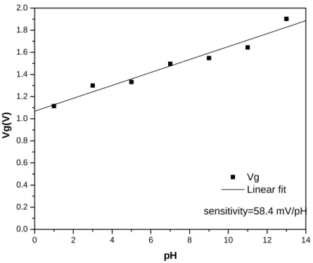
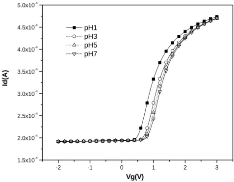
According to I-V curves (Fig4-1), we find some characteristics in our pH-ISFET. When the TaN barrier is under the PE-oxide, the sensitivity is higher and more linear. In the standard pH-ISFET with sensing layer PE-oxide, the sensitivity is very unstable and the range is usually from 30-50 mV/pH [1]. However, the sensitivity in our experiment approaches to 61.2 mV/pH (Fig.4-2) after inserting TaN barrier.
On the other hand, we observe the first and the second measurement at 4 and 6 minutes. Sensitivities are different because of the fast response has not completed [2]. The sensitivity is higher after a long period of time (Fig. 4-3).
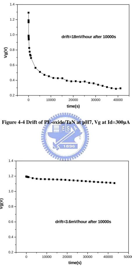
In the discussion of the drift, the standard pH-ISFET with sensing layer PE-oxide always unstable even after several hours [3]. After inserting a TaN barrier, the drift becomes stable (Fig.4-4). It is linear after 10000 seconds although the drift approaches to 18mV/hour. By observing the curve, we find the Vth is graduating lower by the time. We explain the situation for the H+ ions diffusing in the sensing layer and barriers. In the standard pH-ISFET, the drift is unstable because the PE-oxide cannot block ions [4]. After inserting TaN barrier, the ion will be blocked by it.
4-2 The drift and sensitivity characteristics for W
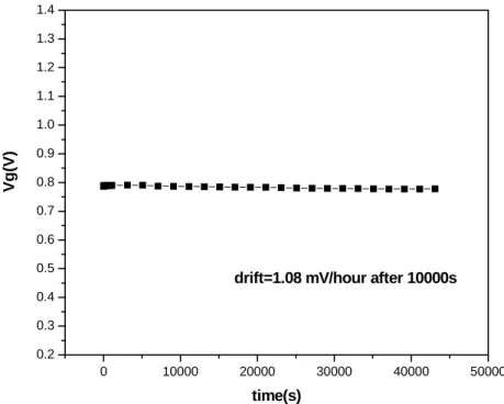
Although TaN can improve the stability of ISFET, the drift is still not good enough. W and WN are barriers we choose to improve the characteristics. For W, the
drift can approach to 3.6mV/hour (Fig. 4-5). Moreover, WN barrier can reduce the drift to 1.08 mV/hour (Fig. 4-6). The results show that different barriers can change the drift characteristic. WN barrier is the best barrier to show the lowest drift in our experiment
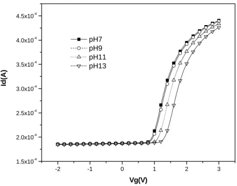
W and WN barrier show lower drift. However, there are different in the response of sensitivities. I-V curves for the W and WN are shown in Fig.4-7 and Fig.4-8. The sensitivity for W from pH1 to pH7 is 49.1 mV/pH (Fig.4-9) but from pH13 to pH7 is 69.1 mV/pH (Fig.4-10). The difference is close to 20 mV/pH. However, there is an opposite situation in the WN. The sensitivity from pH1 to pH7 is 75.8(Fig.4-11) mV/pH but from pH13 to pH7 is 36 mV/pH (Fig.4-12) in WN. Up to now, there is not a clear expression for this phenomenon. In standard theory [5], the surface reaction is the only factor for sensitivity. However, PE-oxide is not a good diffuse barrier so that the diffusion phenomenon has to be considered.
After inserting W and WN barrier under the pH-ISFET with sensing layer low-pressure nitride, the sensitivity is stable (Fig.4-13, Fig.4-14). The drift of WN barrier approaches to 1.44 mV/hour (Fig.4-15) and W barrier approaches to 2.52 mV/hour (Fig.4-16). The drift in the standard pH-ISFET with sensing layer LP-nitride is about 1-2 mV/hour. According to the result, we can conclude that the barrier is more useful to PE-nitride.
4-3 Conclusions
After comparing different barriers, we can give some conclusions:
1. For different barriers, the characteristic of pH-ISFET with sensing layer PE-oxide can be improved.
WN is under the PE-oxide.
3. WN and W barrier have different sensitivities in different pH range.
4-4 References
[1] Li-Te Yin, “Study of indium tin oxide thin film for separative extended gate ISFET”, Materials Chemistry and Physics 70, pp.12–16 2002.
[2] P. Bergveld, “Development of an ion sensitive solid-state device for neurophysiological measurements”, IEEE Trans. Biomed. Eng. 17 pp.70–71,1970
[3] George T. Yu, “Hydrogen ion diffusion coefficient of silicon nitride thin films”, Applied Surface Science 202 pp.68–72, 2002.
[4] H.C.G. Ligtenberg, “solutions for some basic problems of ISFET sensors”, Thesis, Twenty University of Technology, the Netherlands, 1987.
[5] L. Bousse., The role of buried site OH sites in the response mechanism of pH-ISFETs”, Sensors and Actuators B6, pp.65–78 1984.
Chapter 5
Future work
5-1 Future work
In our experiment, barriers can improve the characteristics of the pH-ISFET with sensing layer PE-oxide. Similarly, the other sensing layers with porous structures can be added barriers under the sensing layers. We suppose that is more stable than the original structure.
Although W, TaN and WN get better characteristics, we can attempt other barriers to identify their drifts and sensitivities. Perhaps there will be some barriers better than WN.
In the applications of the ISFET, it always companies with other systems. For example, FIA system contains the channels, ISFET array and circuit on a chip. In our group, we have had the techniques in the channel and circuits. The most important we will do in the future is to integrate all devices in a chip. Although there are still some problems, we believe it is an achievable target in the future.
Figure 1-2 Basic diagram of a back-side contacted ISFET
Figure 2-1 Potential profile and charge distribution at an
oxide electrolyte solution interface
Figure 2-2 Cross section of the standard ISFET
Production method: CZ Type/ Dopant: P/BO
Crystal Axis: <100> Resistivity (ohm-cm):0-100 Diameter (mm): 99.5-100.5 Thickness (μm) :500-550
Figure3-2 Specifications of Wafer
parameters of W sputter parameters of WN sputter
power 150W power 150W
Ar:24sccm Ar: 24sccm N2=4.8sccm
rate=0.3A/s rate=0.4A/s
pre sputter 10min 60W pre sputter 10min 60W
pressure=7.6×10⁻³ pressure=7.6×10⁻³
parameters of Ta sputter parameters of TaN sputter
power 500W power 500W
gas:Ar gas Ar:N2=47:2.6
rate=2.07A/s rate=2.146A/s
pre sputter 5min 300W pre sputter 5min 300W
pressure=7.6×10⁻³ pressure=7.6×10⁻³
parameters of LP-nitride deposition NH3= 17sccm SiH2Cl2=85sccm 18min =1018A temperature=850C pressure=180mT n=2.321
parameters of PE-oxide deposition
temperature=300C TEOS=10sccm
2000A=4 ' 44''
Figure 3-4 Parameters of sensing layers deposition
HDP-RIE
process pressure=10m torr flow rate of CHF3=40sccm
flow rate of Ar=40sccm ICP power=600 Bias power=150 etch time(min) TaN 3' Ta 2' WN 3' W 2' LP 3' PE 2'
-1 0 1 2 3 4 2.0x10⁻⁴ 2.5x10⁻⁴ 3.0x10⁻⁴ 3.5x10⁻⁴ 4.0x10⁻⁴ 4.5x10⁻⁴ 5.0x10⁻⁴ 5.5x10⁻⁴ 6.0x10⁻⁴ Id(A) Vg(V) pH1 pH3 pH3 pH7 pH7 pH9 pH11 pH13
Figure 4-1-1 I-V curves of PE-oxide/TaN from pH1-pH13 after 4 minutes dipping
-1 0 1 2 3 4 2.0x10⁻⁴ 2.5x10⁻⁴ 3.0x10⁻⁴ 3.5x10⁻⁴ 4.0x10⁻⁴ 4.5x10⁻⁴ 5.0x10⁻⁴ 5.5x10⁻⁴ 6.0x10⁻⁴ 6.5x10⁻⁴ pH1 pH3 pH5 pH7 pH7 pH9 pH11 pH13 Id( A ) Vg
0 2 4 6 8 10 12 14 0.0 0.2 0.4 0.6 0.8 1.0 1.2 1.4 1.6 1.8 2.0 sensitivity=58.4 mV/pH Vg (V) pH Vg Linear fit Figure 4-2 Sensitivity of PE-oxide/TaN after 4 minutes dipping
0 2 4 6 8 10 12 14 0.0 0.2 0.4 0.6 0.8 1.0 1.2 1.4 1.6 1.8 2.0 Vg(V) pH Vg Linear fit sensitivity= 61.2mV/pH
0 10000 20000 30000 40000 0.2 0.4 0.6 0.8 1.0 1.2 1.4 Vg( V) time(s) drift=18mV/hour after 10000s
Figure 4-4 Drift of PE-oxide/TaN at pH7, Vg at Id=300µA
0 10000 20000 30000 40000 50000 0.2 0.4 0.6 0.8 1.0 1.2 1.4 drift=3.6mV/hour after 10000s Vg(V ) time(s)
0 10000 20000 30000 40000 50000 0.2 0.3 0.4 0.5 0.6 0.7 0.8 0.9 1.0 1.1 1.2 1.3 1.4
drift=1.08 mV/hour after 10000s
Vg
(V
)
time(s)
Figure 4-6 Drift of PE-oxide/WN at pH7, Vg at Id=300µA
-2 -1 0 1 2 3 1.5x10⁻⁴ 2.0x10⁻⁴ 2.5x10⁻⁴ 3.0x10⁻⁴ 3.5x10⁻⁴ 4.0x10⁻⁴ 4.5x10⁻⁴ 5.0x10⁻⁴ Id( A ) Vg(V) pH1 pH3 pH5 pH7
Figure 4-7-1 I-V curves from pH1-pH7 for PE-oxide/W barrier after 4 minutes dipping
-2 -1 0 1 2 3 1.5x10⁻⁴ 2.0x10⁻⁴ 2.5x10⁻⁴ 3.0x10⁻⁴ 3.5x10⁻⁴ 4.0x10⁻⁴ 4.5x10⁻⁴ 5.0x10⁻⁴ pH1 pH3 pH5 pH7 Id( A ) Vg(V)
Figure 4-7-2 I-V curves from pH1-pH7 for PE-oxide/W barrier after 6 minutes dipping
-2 -1 0 1 2 3 1.5x10⁻⁴ 2.0x10⁻⁴ 2.5x10⁻⁴ 3.0x10⁻⁴ 3.5x10⁻⁴ 4.0x10⁻⁴ 4.5x10⁻⁴ pH7 pH9 pH11 pH13 Id(A ) Vg(V)
Figure 4-7-3 I-V curves from pH7-pH13 for PE-oxide/W barrier after 4 minutes dipping
-2 -1 0 1 2 3 1.5x10⁻⁴ 2.0x10⁻⁴ 2.5x10⁻⁴ 3.0x10⁻⁴ 3.5x10⁻⁴ 4.0x10⁻⁴ 4.5x10⁻⁴ pH7 pH9 pH11 pH13 Id(A ) Vg(V)
Figure 4-7-4 I-V curves from pH7-pH13 for PE-oxide/W barrier after 6 minutes dipping
-1 0 1 2 3 2.0x10⁻⁴ 2.5x10⁻⁴ 3.0x10⁻⁴ 3.5x10⁻⁴ 4.0x10⁻⁴ 4.5x10⁻⁴ 5.0x10⁻⁴ 5.5x10⁻⁴ 6.0x10⁻⁴ 6.5x10⁻⁴ pH1 pH3 pH5 pH7 Id( A ) Vg(V)
Figure 4-8-1 I-V curves for PE-oxide/WN from pH1-pH7 after 4 minutes dipping
-1 0 1 2 3 2.0x10⁻⁴ 2.5x10⁻⁴ 3.0x10⁻⁴ 3.5x10⁻⁴ 4.0x10⁻⁴ 4.5x10⁻⁴ 5.0x10⁻⁴ 5.5x10⁻⁴ 6.0x10⁻⁴ 6.5x10⁻⁴ pH1 pH3 pH5 pH7 Id( A ) Vg(V)
Figure 4-8-2 I-V curves for PE-oxide/WN from pH1-pH7 after 6 minutes dipping
-1 0 1 2 3 2.0x10⁻⁴ 2.5x10⁻⁴ 3.0x10⁻⁴ 3.5x10⁻⁴ 4.0x10⁻⁴ 4.5x10⁻⁴ 5.0x10⁻⁴ 5.5x10⁻⁴ 6.0x10⁻⁴ pH7 pH9 pH11 pH13 Id( A ) Vg(V)
Figure 4-8-3 I-V curves for PE-oxide/WN from pH7-pH13 after 4 minutes dipping
-1 0 1 2 3 2.0x10⁻⁴ 2.5x10⁻⁴ 3.0x10⁻⁴ 3.5x10⁻⁴ 4.0x10⁻⁴ 4.5x10⁻⁴ 5.0x10⁻⁴ 5.5x10⁻⁴ 6.0x10⁻⁴ Id( A ) Vg(V) pH7 pH9 pH11 pH13
Figure 4-8-4 I-V curves for PE-oxide/WN from pH7-pH13 after 6 minutes dipping
1 2 3 4 5 6 7 0.0 0.2 0.4 0.6 0.8 1.0 1.2 1.4 1.6 1.8 2.0 Vg(V) pH sensitivity=49.1mV/pH
1 2 3 4 5 6 7 0.0 0.2 0.4 0.6 0.8 1.0 1.2 1.4 1.6 1.8 2.0 sensitivity=50.5mV/pH pH Vg(V )
Figure 4-9-2 Sensitivity of PE-oxide/W from pH1-pH7 after 6 minutes dipping.
7 8 9 10 11 12 13 0.5 0.6 0.7 0.8 0.9 1.0 1.1 1.2 1.3 1.4 1.5 1.6 1.7 1.8 1.9 2.0 pH sensitivity=69.1mV/pH Vg(V )
7 8 9 10 11 12 13 0.0 0.1 0.2 0.3 0.4 0.5 0.6 0.7 0.8 0.9 1.0 1.1 1.2 1.3 1.4 1.5 1.6 1.7 1.8 1.9 2.0 pH sensitivity=68.6mV/pH Vg (V)
Figure 4-10-2 Sensitivity of PE-oxide/W from pH7-pH13 after 6 minutes dipping.
1 2 3 4 5 6 7 0.0 0.1 0.2 0.3 0.4 0.5 0.6 0.7 0.8 0.9 1.0 1.1 1.2 1.3 1.4 1.5 1.6 1.7 1.8 1.9 2.0 pH sensitivity=71.7mV/pH Vg( V )
Figure 4-11-1 Sensitivity of PE-oxide/WN from pH1-pH7 after 4 minutes dipping.
1 2 3 4 5 6 7 0.0 0.1 0.2 0.3 0.4 0.5 0.6 0.7 0.8 0.9 1.0 1.1 1.2 1.3 1.4 1.5 1.6 1.7 1.8 1.9 2.0 pH sensitivity=75.8mV/pH Vg(V)
Figure 4-11-2 Sensitivity of PE-oxide/WN from pH1-pH7 after 6 minutes dipping. 7 8 9 10 11 12 13 0.0 0.2 0.4 0.6 0.8 1.0 1.2 1.4 1.6 1.8 2.0 pH sensitivity=37.7mV/pH Vg(V)
Figure 4-12-1 Sensitivity of PE-oxide/WN from pH7-pH13 after 4 minutes dipping.
7 8 9 10 11 12 13 0.0 0.2 0.4 0.6 0.8 1.0 1.2 1.4 1.6 1.8 2.0 pH sensitivity=36mV/pH Vg(V)
Figure 4-12-2 Sensitivity of PE-oxide/WN from pH7-pH13 after 6 minutes dipping, -2 -1 0 1 2 3 2.0x10⁻⁴ 2.5x10⁻⁴ 3.0x10⁻⁴ 3.5x10⁻⁴ 4.0x10⁻⁴ 4.5x10⁻⁴ 5.0x10⁻⁴ 5.5x10⁻⁴ Id( A ) Vg(V) pH1 pH3 pH5 pH7
Figure 4-13-1 I-V curves of LP-nitride/W from pH1 to pH7 after 4 minutes dipping
-2 -1 0 1 2 3 2.0x10⁻⁴ 2.5x10⁻⁴ 3.0x10⁻⁴ 3.5x10⁻⁴ 4.0x10⁻⁴ 4.5x10⁻⁴ 5.0x10⁻⁴ 5.5x10⁻⁴ Vg(V) pH1 pH3 pH5 pH7 Id(A)
Figure 4-13-2 I-V curves of LP-nitride/W from pH1 to pH7 after 6 minutes dipping -2 -1 0 1 2 3 2.0x10⁻⁴ 2.5x10⁻⁴ 3.0x10⁻⁴ 3.5x10⁻⁴ 4.0x10⁻⁴ 4.5x10⁻⁴ 5.0x10⁻⁴ Vg(V) pH7 pH9 pH11 pH13 Id( A )
Figure 4-13-3 I-V curves of LP-nitride/W from pH7 to pH13 after 4 minutes dipping
-2 -1 0 1 2 3 2.0x10⁻⁴ 2.5x10⁻⁴ 3.0x10⁻⁴ 3.5x10⁻⁴ 4.0x10⁻⁴ 4.5x10⁻⁴ 5.0x10⁻⁴ Vg(V) pH7 pH9 pH11 pH13 Id(A)
Figure 4-13-4 I-V curves of LP-nitride/W from pH7 to pH13 after 6 minutes dipping 0 2 4 6 8 10 12 14 0.0 0.1 0.2 0.3 0.4 0.5 0.6 0.7 0.8 0.9 1.0 1.1 1.2 1.3 1.4 1.5 1.6 1.7 1.8 1.9 2.0 pH sensitivity=56.5mV/pH Vg(V )
Figure 4-14-1 Sensitivity of LP nitride/W from pH1-pH13 after 4 minutes dipping
0 2 4 6 8 10 12 14 0.0 0.1 0.2 0.3 0.4 0.5 0.6 0.7 0.8 0.9 1.0 1.1 1.2 1.3 1.4 1.5 1.6 1.7 1.8 1.9 2.0 pH sensitivity=57.2mV/pH Vg(V)
Figure 4-14-2 Sensitivity of LP nitride/W from pH1-pH13 after 6 minutes dipping, 0 10000 20000 30000 40000 50000 0.2 0.4 0.6 0.8 1.0 1.2 1.4 Vg (V ) time(s) drift=1.44 mV/hour
0 10000 20000 30000 40000 50000 0.2 0.4 0.6 0.8 1.0 1.2 1.4 time(s) drift=2.52 mV/hour Vg( V )