Figure 4 Shielding effect as a function of angle Thus, we consider the reason for the existence of optimum
length combinations to be that the r4 choke structure is formed equivalently at each structure like the case of chang-ing S1 only. From this figure, it is also confirmed that each peak point value of the shielding effect is abouty35 dB. 5.2. Case of Oblique Position of S2. In order to study the influence of the angle as well as the metal lengths S1 and S2 on the shielding effect, a calculation of the effect of the effect for different choke structures as shown in Table 2 is also carried out, and the results are shown in Figure 4. It is confirmed from this figure that the shielding effect shifts widely with the change of the angle , and also there is an optimum angle which can obtain the maximum shielding effect. As an example, the angle which is practically used in
Ž .
RE-E4 is 30⬚ S1 s 4 mm, S2 s 9 mm . It is therefore concluded through this analysis that the angle of the choke structure which we referred to is designed so that the opti-mum shielding effect can be performed. However, in the case of an oblique position of S2, it should be noticed that the stair-like approximation shown in Figure 4 is adopted to represent an oblique plate because the orthogonal lattice is used in the FDTD analysis.
6. CONCLUSION
In this study, we discuss the shielding effects for the cases of various sizes of metal parts which compose the door seal using the FDTD method. The results indicate the FDTD is available for analyzing these structures. It is confirmed that there exists optimum combinations of the metal length and the angle between S1 and S2, and that the optimum choke structure obtained in this analysis is very similar to the existing choke structure which was experimentally designed to obtain the maximum shielding effect.
In the future, it will be necessary to examine the shielding effect on the more real microwave radiation which includes various modes.
ACKNOWLEDGMENT
The authors wish to thank Dr. T. Abe of Aoyama Gakuin University for his helpful advice.
REFERENCES
1. Kusunoki, Takano et al., ‘‘Leaking Microwave Power Preventive Apparatus for Microwave Ovens Having Periodic Structures,’’
Nat. Tech. Rep., Vol. 22, No. 2, 1976, pp. 1᎐7.
2. Ohkawa, Watabe, and Kikuchi, ‘‘New Type Door Seal for Mi-crowave Oven,’’ Tech. Rep. IEICE, MW79-58, 1979, pp. 31᎐37. 3. Shimizu, Hashimoto et al., ‘‘The Shielding Effect of Wave
Ab-sorber on Leakage from Gaps,’’ Tech. Rep. IEICE, MW83-54, 1983, pp. 39᎐46.
4. Kunz and Luebbers, The Finite Difference Time Domain Method
for Electromagnetics, CRC Press, Boca Raton, FL, 1993.
䊚 1998 John Wiley & Sons, Inc. CCC 0895-2477r98
COPLANAR WAVEGUIDE TO
COPLANAR STRIPS-FED ACTIVE
LEAKY-WAVE ANTENNA
Cheng-Chi Hu,1Christina F. Jou,1Chien-Jen Wang,1 Shing-Horng Lee,2and Jin-Jei Wu3
1Institute of Communication Engineering National Chiao Tung University
Hsinchu, Taiwan, R.O.C. 2
Institute of Electronic Engineering National Chiao Tung University Hsinchu, Taiwan, R.O.C.
3Department of Electric Engineering
Kao Yuan College of Technology & Commerce Luchu, Taiwan, R.O.C.
Recei¨ed 16 April 1998
( )
ABSTRACT: A new acti¨e coplanar wa¨eguide CPW to coplanar ( )
strips CPS -fed microstrip leaky-wa¨e antenna is de¨eloped, which is integrated with a Gunn diode as an acti¨e source. The CPW᎐CPS balun is used to excite the first higher order mode of the microstrip leaky-wa¨e antenna. The acti¨e leaky-wa¨e antenna has a maximum EIRP of 20.4 dBm at 9.759 GHz. The Gunn oscillator frequency is controlled by tuning the Gunn dc bias, and the beam scanning is demonstrated. The measured scanning angle agrees with the prediction; it is close to 12⬚ as the oscillator frequency is tuned from 9.84 to 9.61 GHz. The coplanar structure allows easy integration of many solid-state de¨ices. It is suitable for monolithic power combining and millimeter-wa¨e applications.
䊚 1998 John Wiley & Sons, Inc. Microwave Opt Technol Lett 19: 335᎐338, 1998.
Key words: leaky-wa¨e antenna; CPW; CPS; scanning; Gunn oscillator
I. INTRODUCTION
An integrated active antenna incorporating an active device and planar antenna has become increasingly important in quasioptical communication system design, such as in
imag-w x
ing, power combining, beam scanning, etc. 1᎐3 . Recently, there has been a growing interest in active antenna
integra-w x
tion using the microstrip leaky-wave antenna 4᎐6 . The mi-crostrip leaky-wave antenna has the advantages of a narrow beam, frequency scanning, easy matching, and is suitable for two-dimensional scanning arrays. The microstrip leaky-wave antenna described in this letter is operated in the first higher order mode, and radiates power in the narrow frequency region before cutoff. The characteristic of the microstrip line antenna is determined by its complex propagation constant. The radiation main beam position depends on its operating frequency. Therefore, it can be used as a frequency-scanning
w x
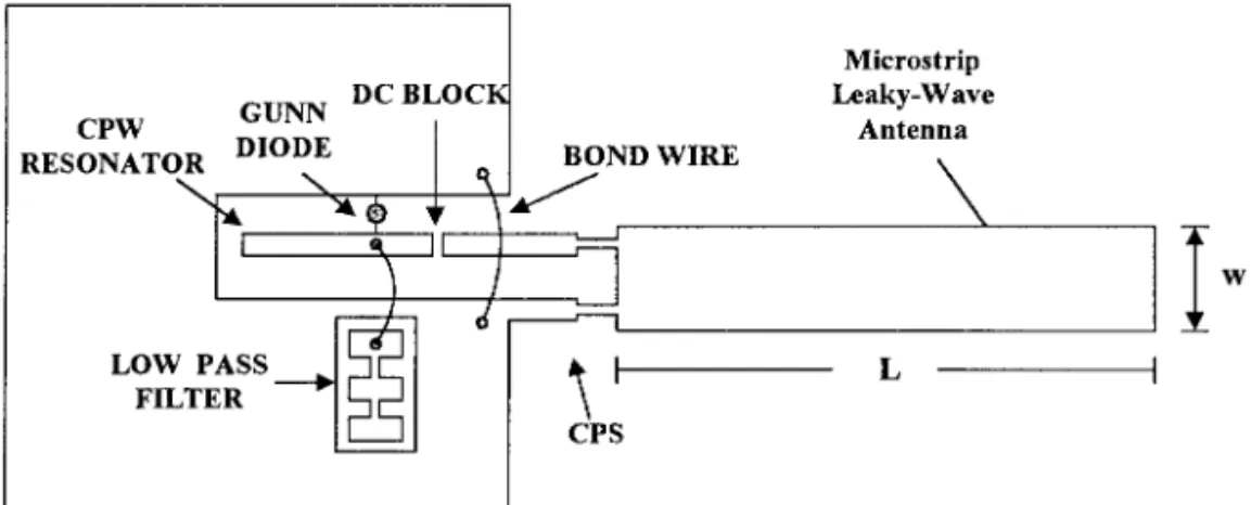
antenna. In 6 , Lin, Sheen, and Tzuang proposed a CPS-fed structure for generating the first higher order mode of the leaky-wave antenna. In this letter, an attempt is made to integrate an active coplanar waveguide to coplanar strips-fed microstrip leaky-wave antenna with a two-terminal device ŽGunn diode. Žsee Fig. 1 . Coplanar waveguide transmission. lines have several features which make them attractive for use in MIC and MMIC structures. Some of the major advan-tages are: easy fabrication, no need for via holes, and being compatible with solid-state devices. In this letter, a transition from CPW to CPS was first built and tested to provide the necessary transformation form the unbalanced CPW feed line to a balanced CPS feed line. In this way, the CPS feed line that feeds the microstrip leaky-wave antenna can excite the first higher order mode. This uniplanar active antenna circuit structure is very suitable for power combining, scan-ning arrays, and communication systems.
II. DESIGN AND MEASUREMENT RESULTS
In order to understand the radiation properties of such a microstrip leaky-wave antenna, we obtained its complex prop-agation constants  y j␣ of the first higher microstrip mode in its leaky range, where is the phase constant and ␣ is the attenuation constant. The complex constants are obtained by
Ž .
employing a rigorous Wiener᎐Hopf solution mentioned by w x7 . Figure 2 shows the variations of phase constant  and attenuation ␣ as a function of frequency. The geometry and coordinate system of the structure are shown in Figure 3. In our structure, the microstrip leaky-wave antenna is open at the top. For values of  - k , power will leak into a spaceo
wave in addition to the surface wave. The space wave actually
Figure 2 Normalized complex propagation constant of the first higher mode for the particular microstrip leaky-wave antenna. hs 0.635 mm, ws 4.2 mm, and⑀ s 10.2. k is the free-space wavenum-r 0 ber
Figure 3 Geometry and coordinate system for the microstrip leaky-wave antenna
corresponds to radiation at some angle ; the value of this angle changes with frequency. By using the approximate
y1Ž .
relationship s cosm rk , where is the angle of theo m
beam maximum measured from the z-axis, we can predict the main beam position.
Figure 1 Configuration of the active CPS-fed microstrip leaky-wave antenna
MICROWAVE AND OPTICAL TECHNOLOGY LETTERS / Vol. 19, No. 5, December 5 1998
Figure 1 shows the active CPW᎐CPS-fed microstrip leaky-wave antenna structure. The circuit consists of a
CPS-Ž .
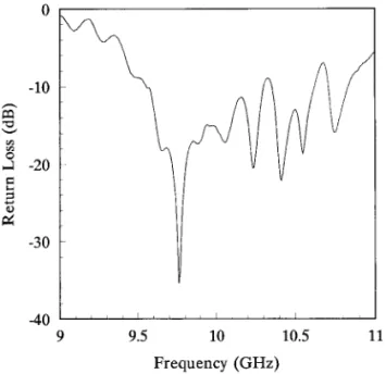
fed microstrip line Ws 0.42 cm, L s 12.7 cm as radiating elements, the CPW᎐CPS transition, and a CPW oscillator integrated with the Gunn diode as the active device. The circuit is designed and fabricated on RTrDuroid 6010 sub-strate with a dielectric constant of 10.2 and a thickness of w x 25 mils. The CPW᎐CPS transition is design based on 8 . Bond wire is placed at the discontinuities to suppress the generation of undesired modes. The return loss of the mi-crostrip leaky-wave antenna was measured with an HP 8720 network analyzer. Figure 4 shows the return loss of the antenna of more than 30 dB at a frequency of 9.759 GHz. CPW was chosen as the oscillator resonator circuit design because of its high Q-factor and easy integration with the active device. The resonant structure is an open-end coplanar waveguide whose length is about 0.5 and 9.759 GHz. The Gunn diode is biased via a bond wire and a high᎐low impedance low-pass filter. A C & K W2420 Gunn diode is integrated with the CPW oscillator circuit.
Figure 5 shows the experiment results of the H-plane patterns for an operating frequency at 9.759 GHz. Figure 5 shows the angle of the beam maximum measured from the z-axis, which is at about 62⬚ with a 3 dB beamwidth of 14⬚.
Ž The bias voltage versus frequency and EIRP effective
.
isotropic radiated power are shown in Figure 6. The bias-turning bandwidth is about 230 MHz centered at 9.759 GHz with a maximum EIRP of 20.4 dBm. As the Gunn bias is varied from 6.5 to 10.5 V, the main beam position changed from 60 to 72⬚. The scanning angle is about 12⬚.
III. CONCLUSION
A new active coplanar waveguide-fed microstrip leaky-wave antenna has been presented. The operation principle for this electronic beam control of the microstrip leaky-wave antenna is described and demonstrated in this letter. The first higher order mode of the microstrip leaky-wave antenna has been efficiently excited by the CPS-fed line. By tuning the Gunn dc bias, beam scanning control of close of 12⬚ is achieved. Such active antenna design as described in this letter is not re-stricted to microwave frequencies, and should be applicable
Figure 4 Measured return loss of the CPW᎐CPS-fed microstrip leaky-wave antenna
Ž .
Figure 5 H-plane y᎐z plane radiation patterns of the active
leaky-wave antenna measured at 9.759 GHz
Figure 6 EIRP and frequency variation versus Gunn bias voltage for active leaky-wave antenna
even up to millimeter-wave frequencies. Furthermore, the circuit is suitable for monolithic applications and power-combining technique due to its planar structure, and it allows easy integration of other solid-state devices, such as the varactor, for wideband electronic frequency tuning. There-fore, this active antenna is also useful for modulated commu-nication links, radar, and other microwave and millimeter-wave applications.
ACKNOWLEDGMENT
This work was supported by National Science Council under Grant NSC86-2215-E009-031.
REFERENCES
1. K. Chang, K. A. Hummer, and J. K. Klein, ‘‘Experiments on Injection Locking of Active Antenna Elements for Active Phased Arrays and Spatial Power Combiners,’’ IEEE Trans. Microwa¨e Theory Tech., Vol. 37, July 1989, pp. 1078᎐1084.
2. D. B. Rutledge and M. S. Muha, ‘‘Image Antenna Arrays,’’ IEEE
Trans. Antenna Propagat., Vol. AP-30, July 1982, pp. 535᎐540.
3. P. Liao and R. A. York, ‘‘A New Phase-Shifterless Beam-Scan-ning Technique Using Arrays of Couple Oscillators,’’ IEEE Trans.
Microwa¨e Theory Tech., Vol. 41, Oct. 1993, pp. 1810᎐1815.
4. A. A. Oliner, ‘‘A New Class of Scannable Millimeter Wave Antennas,’’ Proc. 20th European Microwa¨e Conf., 1990, pp.
95᎐104.
5. G.-J. Chou and C.-K. Tzuang, ‘‘Oscillator-Type Active-Integrated Antenna: The Leaky-Mode Approach,’’ IEEE Trans. Microwa¨e Theory Tech., Vol. 44, Dec. 1996, pp. 2265᎐2272.
6. Y. D. Lin, J. W. Sheen, and C. K. C. Tzuang, ‘‘Analysis and Design of Feeding Structures for Microstrip Leaky Wave An-tenna,’’ IEEE Trans. Microwa¨e Theory Tech., Vol. 44, Sept. 1996,
pp. 1540᎐1547.
7. A. A. Oliner and K. S. Lee, ‘‘Microstrip Leaky Wave Strip Antennas,’’ 1986 IEEE AP-S Int. Symp. Dig., pp. 443᎐446. 8. C. H. Ho, L. Fan, and K. Chang, ‘‘Broad-Band Uniplanar
Hy-brid-Ring and Branch-Line Coupler,’’ IEEE Trans. Microwa¨e Theory Tech., Vol. 41, Dec. 1993, pp. 2116᎐2124.
䊚 1998 John Wiley & Sons, Inc. CCC 0895-2477r98
ON THE BEHAVIOR OF
ELECTROMAGNETIC FIELDS ON THE
INTERFACES OF CHIROSTRIP
DIPOLE ANTENNAS
Feliciano Lumini1and J. C. da S. Lacava2 1
Division of Systems Engineering EMBRAER S. A.
12227-901 Sao Jose dos Campos, SP, Brazil˜ ´ 2Department of Electronic Engineering Instituto Tecnologico de Aeronautica´ ´ 12228-900 Sao Jose dos Campos, SP, Brazil˜ ´
Recei¨ed 14 April 1998
ABSTRACT: Working in the Fourier domain, this paper analyzes the
beha¨ior of electromagnetic fields on the interfaces of chirostrip dipole antennas. Special attention is dedicated to the oscillatory beha¨ior of the kernel of the in¨erse Fourier transform. It was found that the boundary conditions for the magnetic field,¨alid for microstrip structures, are not completely satisfied when we deal with chirostrip structures.䊚 1998 John
Wiley & Sons, Inc. Microwave Opt Technol Lett 19: 338᎐342, 1998. Key words: chirostrip dipoles; near fields; boundary conditions; full-wa¨e spectral-domain analysis
1. INTRODUCTION
During the last ten years, open chirostrip structures have received special attention from the electromagnetics com-munity because of their potential applications in the design of new devices and components. In fact, several canonical problems have been analyzed and reported in the technical
w x
literature 1 . Among them, one should mention the planar
w x w x
single-layered structures 2 , the chirowaveguides 3 , the
rect-w x
angular patches and infinite arrays 4, 5 , and the effects of chiral admittance on radiation patterns, input impedance,
w x
and cross-polarization level of printed dipoles 6, 7 . In spite w x
of numerous works published on this subject 8 , there is not enough information about the characteristics of near electro-magnetic fields in chirostrip antennas.
Using a full-wave spectral-domain analysis method, this work analyzes the behavior of electromagnetic fields on the
interfaces of chirostrip dipole antennas. This means that the electromagnetic fields in the space domain are obtained through double integrals in the Fourier domain. Special
con-w x
siderations are required in this computation 9 . As a result of our calculations, we observed that the chirality causes a rotation in the near-field patterns. Then, at the interface between a perfectly conducting surface and a chiral substrate, the magnetic field component normal to this surface is not null. Moreover, at the interface between a chiral substrate and the free space, the magnetic field component normal to this interface is not continuous even when the magnetic permeability is the same in the two media.
2. THEORY
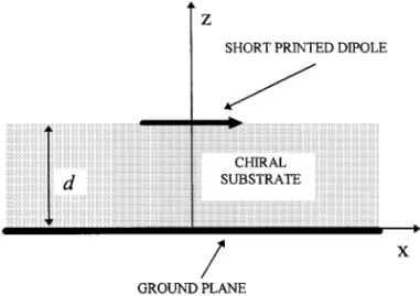
Figure 1 shows the geometry of the problem. A homogeneous isotropic linear chiral medium of thickness d, permittivity⑀ ,c
permeability , and chiral admittance lies on an infinite0 c
perfectly conducting plate, located on the x᎐y plane of a rectangular coordinate system. The planar interface zs d
Ž .
separates the chiral substrate 0- z - d from the free-space
Ž .
region z) d, permittivity ⑀ , and permeability . For0 0
lossless chiral substrate, the parameters ⑀ and are realc c
quantities. The x-directed short dipole is printed on the planar interface at the position xs 0, y s 0, and z s d. As the chiral medium is isotropic, the choice of the dipole direction does not pose any restriction on the present discus-sion. The theory used in this work considers the chirostrip antenna as a boundary problem where the current on the short dipole is the virtual source of the electromagnetic fields. Starting from Maxwell equations and using the Post᎐ Jaggard time-harmonic constitutive relations Ds⑀ E y i Bc c
and Bs H q i E, the wave equations in the chiral0 0 c
layer and in the free-space region are determined. In our approach, the wave equations are solved in the Fourier domain because this technique effectively removes the singu-larity of the spatial Green functions and allows considerable
w x simplification of method of moment calculations 10 . After that, the boundary conditions for the electromagnetic fields are applied at the interfaces zs 0 and z s d, resulting in a set of six equations with six unknowns. Solving this set of equations, the spectral electromagnetic fields in any point of
w x
region zG 0. Following 7, 11 , as the calculations are carried out in the Fourier domain, we obtain the spectral Green functions in compact and closed forms where only sine and cosine functions are present. Finally, to obtain the fields in
Figure 1 X-directed short dipole printed on a ground chiral slab
MICROWAVE AND OPTICAL TECHNOLOGY LETTERS / Vol. 19, No. 5, December 5 1998