Abstract—As the dimensions of semiconductor devices continue
to be reduced, device fluctuations have become critical to deter-mining the accuracy of timing in circuits and systems. This brief studies the discrete-dopant-induced timing characteristic fluctu-ations in 16-nm-gate complementary metal–oxide–semiconductor (CMOS) circuits using a 3-D “atomistic” coupled device–circuit simulation. The accuracy of the simulation has been confirmed by using the experimentally calibrated transistor physical model. For a 16-nm-gate CMOS inverter, 3.5%, 2.4%, 18.3%, and 13.2% normalized fluctuations in the rise time, fall time, high-to-low delay time, and low-to-high delay time, respectively, are found. Random dopants may cause significant timing fluctuations in the studied circuits. Suppression approaches that are based on the circuit and device design viewpoints are implemented to exam-ine the associated characteristic fluctuations. The use of shunted transistors in the circuit provides similar suppression to the use of a device with doubled width. However, both approaches in-crease the chip area. To eliminate the need to inin-crease the chip area, channel engineering approaches (vertical and lateral) are proposed, and their effectiveness in reducing the timing fluctuation is demonstrated.
Index Terms—Fluctuation suppression technique, modeling and
simulation, nanometer-scale metal–oxide–semiconductor field-effect transistor (MOSFET) device and circuit, random dopant effect, timing fluctuation.
I. INTRODUCTION
T
HE GATE lengths of scaled metal–oxide–semiconductor field-effect transistors (MOSFETs) are under 30 nm in 45-nm-node high-performance circuits. Devices with sub-10-nm gate lengths have recently been studied. For state-of-the-art nanometer-scale (nanoscale) circuits and systems, intrinsic device parameter fluctuations that result from line-edge roughness [1], the granularity of the polysilicon gate [2], random discrete dopants [3]–[13], and other causes have substantially affected the signal system timing [10], [11] and high-frequency characteristics [12], [13]. Yield analysis and optimization, which take into account the manufacturing tolerances, model uncertainties, fluctuations in process param-eters, and other factors, are known as indispensablecompo-Manuscript received October 30, 2008; revised February 14, 2009. Current version published May 15, 2009. This work was supported in part by Taiwan National Science Council (NSC) under Contract NSC-97-2221-E-009-154-MY2 and Contract NSC-96-2221-E-009-210 and in part by Taiwan Semicon-ductor Manufacturing Company, Hsinchu, Taiwan, under a 2007–2008 grant. This paper was recommended by Associate Editor P. Kinget.
Y. Li is with the Department of Communication Engineering, National Chiao Tung University, Hsinchu 300, Taiwan, and also with the National Nano Device Laboratories, Hsinchu, Taiwan (e-mail: [email protected])
C.-H. Hwang and T.-Y. Li are with the Department of Communication Engineering, National Chiao Tung University, Hsinchu 300, Taiwan.
Color versions of one or more of the figures in this paper are available online at http://ieeexplore.ieee.org.
Digital Object Identifier 10.1109/TCSII.2009.2019168
nents of the circuit design procedure [14]–[17]. Among the aforementioned fluctuation sources, the random dopant effect is caused by the scaled device dimensions. The randomness of the dopant position and number in a device makes the fluctuation of device characteristics difficult to model and mitigate. Diverse approaches have recently been presented to investigate fluctuation-related issues in semiconductor devices [3]–[10] and circuits [10]–[13]. However, less attention has been paid to timing characteristic fluctuations of active devices caused by random dopants. Additionally, the randomness of dopant positions in devices makes the fluctuation of the gate capacitance of a device nonlinear and difficult to model using the present compact models [5]. Thus, this brief presents a large-scale statistically sound coupled device–circuit simula-tion approach to analyze the random dopant effect in nanoscale complementary metal–oxide–semiconductor (CMOS) circuits, concurrently capturing the fluctuations associated with the number and positions of discrete dopants. Various fluctuation suppression approaches have been proposed [6]–[9], [12], [13]. Unfortunately, the effect of such suppression techniques on transient timing fluctuations is not yet clear. To mitigate the impact of timing fluctuations on the circuit, four fluctuation suppression techniques from the circuit and device design view-points are proposed and implemented. Relationships between the suppression of dc and transient characteristic fluctuations are thus studied. The results of this brief elucidate the fluctua-tions in circuit characteristics and support the development of the next-generation of nanoelectronic circuits and systems.
This brief is organized as follows: Section II introduces the simulation technique for studying the effect of random dopants in nanoscale devices and circuits. Sections III and IV study the characteristic fluctuations and associated suppression techniques for 16-nm devices and circuits. Finally, conclusions are drawn, and future work is suggested.
II. NANO-MOSFET CIRCUIT ANDSIMULATION
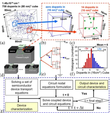
The nominal channel doping concentration of the explored device is 1.48× 1018 cm−3. They have a 16-nm gate, a gate
oxide thickness of 1.2 nm, and a workfunction of 4.4 eV. The source/drain and background doping concentrations are 1.1× 10²⁰and 1× 1015cm−3, respectively. To study the effect of random fluctuations in the number and position of discrete dopants in the channel region, 758 dopants are randomly gen-erated in an (80 nm)3 cube, yielding an equivalent doping concentration of 1.48× 1018 cm−3, as shown in Fig. 1(a). The (80 nm)3 cube is then partitioned into 125 subcubes of volume (16 nm)3. The number of dopants varies from zero to 14, and the average number is six, as presented in Fig. 1(b), (c), and (f). These 125 subcubes are then mapped into the
Fig. 1. (a) Discrete dopants randomly distributed in the (80 nm)3 cube with the average concentration of 1.48× 1018 cm−3. (b)–(d) There are
758 dopants within the cube, but dopants vary from 0 to 14 (the average number is six) within its 125 subcubes of volume (16 nm)3. (e) and (f) One hundred twenty-five subcubes are mapped into the channel region for dopant-position/number-sensitive device simulation and coupled device–circuit simu-lation. (g) Simulation flowchart for the coupled device–circuit approach.
channel region of the device for the 3-D “atomistic” device simulation, including discrete dopants, as shown in Fig. 1(d). The device is simulated by solving a set of 3-D density-gradient equations coupled with the Poisson equation and electron–hole current continuity equations [18]. In the “atomistic” device simulation, the resolution of individual charges within a con-ventional drift–diffusion simulation using a fine mesh creates problems associated with singularities in the Coulomb potential [3]. Thus, the density-gradient approximation is used to handle discrete charges by properly introducing the related quantum mechanical effects [18]. The inverter circuit, as displayed in Fig. 1(e), is used as a tested circuit to study the fluctuation of timing characteristics. Similarly, 125 cases of PMOSFETs with discrete dopants are generated according to Fig. 1(a)–(d). Then, 125 pairs of NMOSFETs and PMOSFETs are randomly selected and used to study the circuit characteristic fluctuations. To fairly compare the NMOSFET- and PMOSFET-induced characteristic fluctuations and eliminate the effect of the tran-sistor size on the fluctuation, the dimensions of the PMOSFET were the same as those of the NMOSFET, and the absolute value of the nominal threshold voltages for both the NMOSFET and PMOSFET were both 140 mV. All statistically generated devices and circuits with discrete dopants, as shown in Fig. 1, are incorporated into the large-scale 3-D coupled device–circuit simulation, which is performed using a parallel computing system [19]. In estimating circuit characteristics, since no well-established compact model of ultrasmall nanoscale devices is available, to capture the discrete-dopant-position-induced fluc-tuations, a device–circuit coupled simulation approach [20] is employed, as shown in Fig. 1(g). The characteristics of the de-vices of the test circuit are first estimated by solving the device
Fig. 2. (a) ID−VGand (b) C−V curves for the studied 16-nm-gate
transis-tors with discrete dopant fluctuations.
transport equations. The obtained result is then used as initial guesses in the coupled device–circuit simulation. The nodal equations of the test circuit are formulated and then directly coupled to the device transport equations (in the form of a large matrix that contains both circuit and device equations), which are simultaneously solved to obtain the circuit characteristics. The device characteristics, such as distributions of potential and current density, obtained by device simulation are input in the circuit simulation through device contacts. The effect of discrete dopants in the transistor on circuit characteristics is thus properly estimated. The characteristic fluctuation of the device was validated with reference to the experimentally measured data [7] to ensure the best accuracy.
III. INTRINSICDEVICE ANDCIRCUITFLUCTUATIONS IN
NANOSCALEMOSFETs
Fig. 2(a) plots the ID−VG characteristics of 16-nm planar
NMOSFETs with discrete dopant fluctuations; the solid line represents the nominal case (continuously doped channel with a doping concentration of 1.48× 1018 cm−3), and the dashed lines are random-dopant-fluctuated devices. For the device with between 0 and 14 discrete dopants, the threshold voltage fluc-tuation σVthis about 58.5 mV, which may resulted in 7.9% and 54.5% fluctuations inON- andOFF-state currents, respectively. Fig. 2(b) plots the capacitance–voltage (C−V ) characteristics of the studied transistors. The C−V curves are horizontally shifted due to the variation of the effective channel doping concentration, which may be described using the corresponding
Vth parameters in a compact model. Additionally, the shape of the curves is changed due to the randomness of the dopant position in the channel, which affects the shape of the depletion region [5]. To the best of the authors’ knowledge, the fluctu-ation in the gate capacitance Cg has not yet been modeled,
and a coupled device–circuit simulation must be performed to estimate it. The normalized Cg fluctuation is then calculated
as a function of the gate bias, and the normalized maximum variation of Cg is about 18.9%. The discrete dopant effect not
only causes fluctuations in Vthand current but also affects the gate capacitance of the transistor. Therefore, the transistor’s intrinsic gate capacitance is used as a load capacitance herein, and the intrinsic timing fluctuations that are induced by discrete dopants are focused. Fig. 3 plots the input and output transition characteristics for the inverter circuit. Fig. 3(a) presents the input and output signals; the solid line represents the nominal case (continuously doped channel with a channel doping con-centration of 1.48× 1018cm−3), and the dashed lines represent cases with discrete dopant fluctuations. The rise time tr, fall
time tf, and hold time of the input signal are 2, 2, and 30 ps,
Fig. 3. (a) Input and output signals for the studied discrete-dopant-fluctuated 16-nm-gate inverter circuit. Zoom-in plots of the (b) fall and (c) rise transitions. (d) Summarized timing fluctuations in the 16-nm-gate inverter circuit.
falling and rising transitions, respectively. The term tr is the
time required for the output voltage VOUT to rise from 10% of the logic “1” level to 90% of the same level, and tf denotes
the time required for the output voltage to fall from 90% of the logic “1” level to 10% of the same level. The low-to-high delay time tLH and high-to-low delay time tHL are defined as the difference between the times of the 50% points of the input and output signals during the rising and falling of the output signal, respectively. Fig. 3(d) plots the normalized tim-ing characteristic fluctuations (the standard deviation/nominal value × 100%). For the 16-nm-gate CMOS inverter, as the number of discrete dopants varies from 0 to 14, normalized fluctuations of tr, tf, tHL, and tLH, of 3.5%, 2.4%, 18.3%, and 13.2%, respectively, may occur. The delay time fluctuations dominate the timing characteristics. The normalized maximum fluctuations (the maximum variation of time/nominal value× 100%) of the high-to-low and low-to-high delay times are about 101.8% and 73.5%, respectively. Notably, the maxi-mum and minimaxi-mum delays associated with this specific set of 125 randomized channels would vary such that their range would increase as the number of samples increased. For the high-to-low signal transition of the output signal, the delay time is dominated by the starting points of the signal transition and then controlled by theON/OFFstate of the NMOSFETs in the inverter circuit. Therefore, the fluctuation of the threshold voltage of NMOSFETs substantially affects the high-to-low delay time characteristic. Similarly, the low-to-high delay time fluctuation is strongly influenced by the σVth of PMOSFETs. σtHL exceeds σtLHbecause the σVthof NMOSFETs exceeds that of PMOSFETs. The σVthof NMOSFETs is larger because the majority carriers of NMOSFETs have a smaller effective mass and, thus, exhibit a larger mobility fluctuation than those of PMOSFETs. The rise/fall time fluctuations depend on the charge/discharge capability of the PMOSFETs/NMOSFETs. Therefore, σtr exceeds σtf because the driving capability of
PMOSFETs is weaker than that of NMOSFETs in the given device dimensions scenario. The device with larger driving
Fig. 4. (a) Rise/fall time and (b) low-to-high and high-to-low delay times for the studied discrete-dopant-fluctuated 16-nm-gate inverter circuit, where the inset shows the inverter with shunted NMOSFETs for mitigating the timing fluctuations induced by NMOSFETs.
capability requires less time to charge and discharge a given load capacitance and, thus, exhibits less fall time fluctuations. The rise and fall time fluctuations, in general, may not be as important as the delay time fluctuation in circuit timing; how-ever, their maximum variations can exceed 0.237 and 0.110 ps, respectively, which exceed the delay time fluctuation and should therefore be considered in statistical timing analysis in circuit and system design. Moreover, fluctuations in the rise and fall times can be added to the delay time, thus increasing the delay time fluctuations.
IV. FLUCTUATIONSUPPRESSIONTECHNIQUES
In the study of fluctuation suppression techniques, since
σtHL is a dominating factor in timing fluctuations and the PMOSFET is used as the control, the fluctuation suppression techniques are only applied to NMOSFETs.
A. Circuit-Level Suppression
From the circuit design viewpoint, an inverter with shunted NMOSFETs is proposed to mitigate the fluctuations in the timing characteristics that are induced by NMOSFETs, as shown in the inset of Fig. 4(a). Fig. 4(a) compares tr and tf
Fig. 5. Comparison of the (a) high-to-low and (b) low-to-high delay times for the (dashed lines) original inverter circuit and (solid lines) inverter circuit with shunted NMOSFETs.
circuits. Since the number of NMOSFETs used to discharge the load capacitance is increased with respect to the original inverter, the nominal value and the fluctuations of the fall time are reduced. However, the increased number of transistors increased the load capacitance and the number of fluctuation sources, affecting the rise time and its fluctuations. Fig. 4(b) compares tLH, tHL, and their fluctuations. tHL, σtHL, and σtHLare reduced in the shunted NMOSFETs inverter circuits. Fig. 5(a) and (b) compares the high-to-low and low-to-high transitions for the original inverter and the shunted NMOSFETs inverter circuits, respectively. Since the high-to-low transition begins when one of the NMOSFETs is turned on, the tHL and σtHL of the shunted NMOSFETs inverter are smaller than the original inverter because the shunted NMOSFETs inverter has a higher probability of having a low Vth NMOSFET than the original inverter. The tHL of the inverter is possibly reduced with a low Vth NMOSFET shunted. The range of spread of tHLis therefore reduced. Similarly, in a low-to-high transition, since the driving capability of PMOSFETs is lower than that of NMOSFETs, the rise transition starts when both of the shunted NMOSFETs are turned off. The tLHof the inverter is possibly to be increased with a high Vth NMOSFET shunted, and therefore, the range of spread of tLHis reduced. However, since the probability that the inverters with low Vth NMOSFETs is reduced, tLH is significantly increased, as shown in Fig. 4(b). From the device design viewpoint, the inverter with the shunted transistors can be implemented by designing NMOSFETs with a double device width. The following simple analytical expression reveals that a device with large dimensions has a small threshold voltage fluctuation [6]:
σVth= 3.19× 10⁻⁸
tox√NA0.401
W L [V] (1)
where toxis the thickness of gate oxide; W and L are the width and length of the transistor, respectively. To compare the device characteristics on a fair basis, the nominal threshold voltages for devices with doubled width are calibrated to 140 mV. Fig. 6(a) and (b) displays the normalized rise/fall time and delay time for the original inverter, the inverter with the shunted NMOSFETs, and inverter with doubled NMOSFET width. As expected, the timing characteristics of the inverter with doubled NMOSFET width are similar to that of the inverter with the shunted NMOSFETs. The high-to-low timing characteristics of the inverter with doubled NMOSFET width are improved at the cost of a worse low-to-high signal transition. Notably, both approaches [i.e., (B) and (C)] may increase the short-circuit leakage power and chip area, potentially limiting the use of these fluctuation suppression techniques.
Fig. 6. Normalized (a) rise/fall time and (b) delay time for the (A) original inverter, (B) inverter with the shunted NMOSFETs, and (C) inverter with doubled NMOSFET width.
Fig. 7. Proposed (a) vertical doping profile engineering and (b) lateral asym-metry doping profile to suppress random dopant fluctuations.
B. Device-Level Suppression
To prevent the increase of the chip area, two channel engi-neering approaches (the vertical doping profile engiengi-neering and the lateral asymmetry doping profile, as shown in Fig. 7(a) and (b), respectively) are proposed to reduce the device and circuit characteristic fluctuations. As in the original doping profile, the numbers of channel dopants in the vertical doping profile engineering and the lateral asymmetry doping profile vary from 0 to 14; the average in each case is six. Similarly, to compare the device characteristics on a fair basis, the nominal threshold voltages of devices with channel engineering are calibrated to 140 mV, which is the same nominal threshold voltage as in the original cases. Notably, the effect of channel engineering approaches cannot be predicted by (1), and therefore, the cou-pled device–circuit simulation approach is adopted to examine their effectiveness. For the vertical doping profile engineering, the doping profile from the device surface to the substrate follows the normal distribution. The characteristic fluctuation is suppressed because fewer fluctuation sources (i.e., the discrete dopants) are located closer to the current-conducting path. In the lateral asymmetry doping profile, unlike the profiles of con-ventional lateral asymmetry devices with higher channel doping concentrations nearer the source end of the channel region, the channel doping concentration is higher when the dopants are nearer the drain end of the channel region. Dopants at the source end of the channel may induce a larger current fluctuation than they do at the drain end of the channel. Moreover, in the proposed lateral asymmetry doping profile, since most of the dopants are located near the drain end of the channel, the gate-to-drain capacitance Cgd fluctuation becomes the major
source of the gate capacitance fluctuation. The gate-to-drain capacitance and its fluctuation are significantly suppressed with the increasing drain bias due to the increased depletion width close to the drain end of the channel region.
Table I summarizes the improvement of the timing char-acteristic fluctuations and nominal timing charchar-acteristics as-sociated with the fluctuation suppression techniques from the
circuit (A: inverter with shunted NMOSFETs) and the device design viewpoints (B: inverter with doubled NMOSFET width; C: inverter with vertical doping profile engineering; and D: inverter with the lateral asymmetry doping profile). The “+” and “−” signs in the nominal timing characteristic indicate the increase and decrease of the corresponding timing character-istics, respectively. The “−” sign in the timing characteristic fluctuations represents the degradation of the corresponding timing characteristics. To improve high-to-low transition char-acteristics and reduce high-to-low timing fluctuations, the use of shunted NMOSFETs (A) and an increase in NMOSFET width (B) can be considered at the cost of worse low-to-high transition characteristics and increased chip area and power. In reducing delay time fluctuations, the lateral asymmetry doping profile (D) is the most effective. However, a large short-channel effect of the device and the consumption of leakage power should be considered. Without scarifying the chip area and device performance, vertical doping profile engineering (C) is effective for low-power applications.
V. CONCLUSION
In this brief, a 3-D “atomistic” coupled device–circuit simulation approach has been adopted to investigate the random-dopant-induced timing characteristic fluctuations in nanoscale CMOS inverter circuits, concurrently capturing the discrete-dopant-number- and discrete-dopant-position-induced fluctuations. The experimentally calibrated simulation tech-nique predicted that the discrete-dopant-fluctuated 16-nm CMOS inverter circuit may exhibit 3.5%, 2.4%, 18.3%, and 13.2% normalized fluctuations in the rise time, fall time, high-to-low delay time, and low-to-high delay time, respectively. To suppress the discrete-dopant-induced timing fluctuations, four suppression techniques from the circuit and device design viewpoints have been examined. This brief provides an insight into random-dopant-induced timing characteristic fluctuations, which may benefit the development of state-of-the-art digital circuits with robust timing characteristics. This approach can further be used to study the intrinsic parameter fluctuations in various digital, analog/RF, and memory circuits.
[3] N. Sano, K. Matsuzawa, M. Mukai, and N. Nakayama, “Role of long-range and short-long-range Coulomb potentials in threshold characteristics under discrete dopants in sub-0.1 μm Si-MOSFETs,” in IEDM Tech. Dig., Dec. 2000, pp. 275–278.
[4] H.-S. Wong, Y. Taur, and D. J. Frank, “Discrete random dopant dis-tribution effects in nanometer-scale MOSFETs,” Microelectron. Reliab., vol. 38, no. 9, pp. 1447–1456, Sep. 1999.
[5] A. Brown and A. Asenov, “Capacitance fluctuations in bulk MOSFETs due to random discrete dopants,” J. Comput. Electron., vol. 7, no. 3, pp. 115–118, Sep. 2008.
[6] A. Asenov and S. Saini, “Suppression of random dopant-induced thresh-old voltage fluctuations in sub-0.1-μm MOSFETs with epitaxial and δ-doped channels,” IEEE Trans. Electron Device, vol. 46, no. 8, pp. 1718– 1724, Aug. 1999.
[7] Y. Li, S.-M. Yu, J.-R. Hwang, and F.-L. Yang, “Discrete dopant fluctuated 20 nm/15 nm-gate planar CMOS,” IEEE Trans. Electron Device, vol. 55, no. 6, pp. 1449–1455, Jun. 2008.
[8] Y. Li and S.-M. Yu, “A coupled-simulation-and-optimization approach to nanodevice fabrication with minimization of electrical characteristics fluctuation,” IEEE Trans. Semicond. Manuf., vol. 20, no. 4, pp. 432–438, Nov. 2007.
[9] Y. Li and C.-H. Hwang, “Discrete-dopant-induced characteristic fluctua-tions in 16 nm multiple-gate silicon-on-insulator devices,” J. Appl. Phys., vol. 102, no. 8, p. 084 509, Oct. 2007.
[10] H. Mahmoodi, S. Mukhopadhyay, and K. Roy, “Estimation of delay variations due to random-dopant fluctuations in nanoscale CMOS cir-cuits,” IEEE J. Solid-State Circuits, vol. 40, no. 9, pp. 1787–1796, Sep. 2005.
[11] X. Tang, K. A. Bowman, J. C. Eble, V. K. De, and J. D. Meindl, “Impact of random dopant placement on CMOS delay and power dissipation,” in Proc. 29th Eur. Solid-State Device Res. Conf., Sep. 1999, pp. 184–187. [12] Y. Li and C.-H. Hwang, “High-frequency characteristic fluctuations of
nano-MOSFET circuit induced by random dopants,” IEEE Trans. Microw. Theory Tech., vol. 56, no. 12, pp. 2726–2733, Dec. 2008.
[13] Y. Li, C.-H. Hwang, T.-C. Yeh, H.-M. Huang, T.-Y. Li, and H.-W. Cheng, “Reduction of discrete-dopant-induced /high-frequency characteristic fluctuations in nanoscale CMOS circuit,” in Int. Conf. Simul. Semicond. Process. Devices, Sep. 2008, pp. 209–212.
[14] J. Jaffari and M. Anis, “Variability-aware bulk-MOS device design,” IEEE Trans. Comput.-Aided Design Integr. Circuits Syst., vol. 27, no. 2, pp. 205–216, Feb. 2008.
[15] L. Brusamarello, R. da Silva, G. I. Wirth, and R. A. L. Reis, “Probabilis-tic approach for yield analysis of dynamic logic circuits,” IEEE Trans. Circuits Syst. I, Reg. Papers, vol. 55, no. 8, pp. 2238–2248, Sep. 2008. [16] H. Nho, S.-S. Yoon, S. S. Wong, and S.-O. Jung, “Numerical estimation
of yield in sub-100-nm SRAM design using Monte Carlo simulation,” IEEE Trans. Circuits Syst. II, Exp. Briefs, vol. 55, no. 9, pp. 907–911, Sep. 2008.
[17] P.-R. Kinget, “Device mismatch and tradeoffs in the design of analog circuits,” IEEE J. Solid-State Circuits, vol. 40, no. 6, pp. 1212–1224, Jun. 2005.
[18] M. G. Ancona and H. F. Tiersten, “Macroscopic physics of the silicon inversion layer,” Phys. Rev. B, Condens. Matter, vol. 35, no. 15, pp. 7959– 7965, May 1987.
[19] Y. Li, H.-M. Lu, T.-W. Tang, and S. M. Sze, “A novel parallel adap-tive Monte Carlo method for nonlinear Poisson equation in semicon-ductor devices,” Math. Comput. Simul., vol. 62, no. 3–6, pp. 413–420, Mar. 2003.
[20] T. Grasser and S. Selberherr, “Mixed-mode device simulation,” Micro-electron. J., vol. 31, no. 11/12, pp. 873–881, Dec. 2000.