低溫多晶矽薄膜電晶體元件特性分布於用電路模擬之研究
69
0
0
全文
(2) 低溫多晶矽薄膜電晶體元件特性分布 用於電路模擬之研究 Study on the Characteristics Distributions of LPTS TFTs for Circuit Simulation 研 究 生:彭國烽. Student : Guo-Feng Peng. 指導教授:陳志隆 博士. Advisor : Dr. Jyh-Long Chern. 戴亞翔 博士. Dr. Ya-Hsiang Tai. 國 立 交 通 大 學 光電工程學系 光電研究所碩士班 碩 士 論 文 A Thesis Submitted to Department of Photonics Institute of Electro-Optical Engineering College of Electrical Engineering and Computer Science National Chiao Tung University in Partial Fulfillment of the Requirements for the Degree of Master in Electro-Optical Engineering June 2006 Hsinchu, Taiwan, Republic of China. 中 華 民 國 九 十 五 年 六 月.
(3) 低溫多晶矽薄膜電晶體元件特性分布 用於電路模擬之究研. 研究生:彭國烽. 指導教授: 陳志隆 博士 戴亞翔. 博士. 國立交通大學 光電工程學系光電工程研究所. 摘要. 多晶矽薄膜電晶體(poly-Si TFTs)基於其優於非晶矽薄膜電晶體(amorphous silicon TFTs)的電流驅動能力,最近在液晶顯示器(AMLCD)及有機發光二極體 (AMOLED)顯示器的週邊電路整合應用上皆備受矚目。在本文中,我們將對低 溫多晶矽薄膜電晶體(low temperature poly-Si TFTs)的元件特性作一統計性的研 究。對於在固定距離下兩元件間特性如臨界電壓(threshold voltage)及遷移率 (mobility)之差異,會做進一步的討論。這些元件間差異行為的變異性(variation) 分布將可以用我們所提出的數學模型加以描述,取代之前所廣泛採用的高斯分 布。而在這些我們所提出函數對於實際量測到的分布之比較中,經過回歸分析所 得之回歸變異係數(R square)皆在 0.95 之上。此一結果代表我們所提出的變異性 的模型與實際分布情況十分吻合,也反映出該模型的適用性。更進一步的,本文 所提出的模型會用於在積體電路中常用到的差動對(differentia pair)電路與電流 鏡(current mirror)電路之模擬。我們將可以從模擬的結果之中,了解電路上元件. I.
(4) 間的變異性對電路性能產生之影響。而從模擬結果,我們發現電晶體變異性行 為,也可以藉由定義原始資料的四分位差值來描述,與函數並無絕對相關,並且 也可以得到一個與真實分布類似的分布。因此我們在一般商用模擬軟體中,仍然 可以採用高斯分布來進行電路模擬,並可以得到比過去更加精準的模擬結果。. II.
(5) Study on the Characteristics Distributions of LTPS TFTs for Circuit Simulation. Student : Guo-Feng Peng. Advisor : Dr. Jyh-Long Chern Dr. Ya-Hsiang Tai. Department of Photonics & Institute of Electro-optical Engineering, National Chiao Tung University. Abstract. Low Temperature Polycrystalline Silicon (LTPS) thin film transistors (TFTs) have attracted much attention in the application on the integrated peripheral circuits of display electronics such as active matrix liquid crystal displays (AMLCDs) and active matrix organic light emitting diodes (AMOLEDs) due to its better current driving compared with a-Si (amorphous silicon) TFTs. In this thesis, the variation characteristics of LTPS TFTs are statistically investigated. The differences of the threshold voltage and mobility with the same device distance are further studied. The difference shows the distribution much centered than the Gaussian distribution and a proper model is proposed to describe the variation behaviors with difference device distances, for which the R squares (Coefficient of Determination) are higher than 0.95, reflecting the validity of the model. Furthermore, the proposed models are used to simulate the performance of the differential pair and current mirror circuit, which are. III.
(6) commonly used in VLSI. Simulation results show the effects of the variation behavior on the estimation of the circuit performance. Besides, from the simulation results, it is found that the Gaussian distributions defined by the inter-quartile range of parameters difference data have a good fitness for the real data distribution compared with Gaussian distribution defined by the standard deviation. Therefore, Monte Carlo analysis with Gaussian distribution still can be used to simulate LTPS TFT circuits in simulation tools. Furthermore, the circuit simulation results will be more accurate than before.. IV.
(7) 誌. 謝. 在這二年研究生涯中,最要感謝的是我的指導教授戴亞翔老師, 總是充滿愛心與耐心的指導我,不論是課業或生涯規劃上,都帶給我 許多的幫助。還有要感謝冉曉雯老師,謝謝妳的關心與貼心,讓我順 利的完成課業,我會加油的。 除此之外,還要感謝學長們在我研究方向及專業領域的指導與協 助。也要感謝同實驗室的同學、學弟,不管在研究上、生活上,你們 都帶給我許多歡樂與幫助,並陪著我共同度過這段時光。 最後要感謝的是我的父母與家人,還有可愛的女友麵包,因為有 你們在背後默默支持與加油,才有今日的我。我愛你們,謝謝你們。 最後,僅以此論文獻給你們。 國烽 2006.06. V.
(8) Contents Chinese Abstract ………………………….……………………………………... I English Abstract …………………………………………..…………..……….. III Acknowledgement ……..………………………………...…………………....... V Contents ……………………………………………………………….……….... VI Figure Captions …………………………………………………………….... VIII. Chapter 1. Introduction 1-1. Introduction to LTPS TFT technology ………….………………..…………1 1-2. Device variation …………...……………………………………………..…2 1-3. Motivation …………………………………………………………………..3 1-5. Thesis outline ……………………………………………………………….3. Chapter 2. Statistical analysis of crosstie TFT device parameters 2-1. Introduction to crosstie TFTs ……………………………………………….5 2-2. Device fabrication and parameter extraction ……………………………….6 2-2-1. Device fabrication …………………………………………………...6 2-2-2. Parameter extraction ……...…………………………………………7 2-3. N-type TFT & P-type TFT 2-3-1. Initial parameter distribution ………………………………………..8 2-3-2. The distribution of initial parameter difference with different device distance ……………………………………………………………10 2-3-3. The models of distributions ………………………………………..11 2-4. The distribution comparison between N-type TFT and P-type TFT……….14. Chapter 3. Effects of device distribution on circuit performance 3-1. Introduction to the differential pair and current mirror ...………………….15 VI.
(9) 3-2. Evaluation of the circuit performance with proposed models and other simulation skills ……………………………………………………………16 3-3. Discussion and conclusion ………………………………………………...18. Chapter 4. Conclusion …………………………………………………………21 References ………………………………………………………………………...23 Figures ......................................................................................................................24 Vita ............................................................................................................................59. VII.
(10) Figures Captions Chapter 1 Fig. 1-1 The block diagram of an active matrix display Fig. 1-2 The integration of peripheral circuits in a display achieved by poly-Si TFTs Fig. 1-3 The initial characteristics of LTPS TFTs are different from one another due to various distributions of grain boundaries. Chapter 2 Fig. 2-1 The layout of the crosstie TFTs Fig. 2-2 The schematic cross-section structure of the N-type poly-Si TFT with lightly doped drain Fig. 2-3 The schematic cross-section structure of the P-type poly-Si TFT Fig. 2-4 (a) The distributions of threshold voltage for N-type TFTs Fig. 2-4 (b)The distributions of mobility for N-type TFTs Fig. 2-4 (c)The distributions of subthreshold for N-type TFTs Fig. 2-5 (a)The distributions of threshold voltage for P-type TFTs Fig. 2-5 (b)The distributions of mobility for P-type TFTs Fig. 2-5 (c)The distributions of subthreshold for P-type TFTs Fig. 2-6 The threshold voltage distribution along the device position Fig. 2-7 Simulation of the threshold voltage distribution along the device position for a long range Fig. 2-8 (a) The average and the standard deviation of the threshold voltage differences of N-type TFTs Fig. 2-8 (b) The average and the standard deviation of the mobility differences of N-type TFTs Fig. 2-8 (c) The average and the standard deviation of the subthreshold swing VIII.
(11) differences of N-type TFTs Fig. 2-9 (a) The average and the standard deviation of the threshold voltage differences of P-type TFTs Fig. 2-9 (b) The average and the standard deviation of the mobility differences of P-type TFTs Fig. 2-9 (c) The average and the standard deviation of the subthreshold swing differences of N-type TFTs Fig. 2-10 (a) The distribution of Vth difference of N-type TFT and its fitting curve under the device distance of 40 µm Fig. 2-10 (b) The distribution of Vth difference of N-type TFT and its fitting curve under the device distance of 200 µm Fig. 2-10 (c) The distribution of Vth difference of N-type TFT and its fitting curve under the device distance of 2000 µm Fig. 2-10 (d) The distribution of Vth difference of P-type TFT and its fitting curve under the device distance of 40 µm Fig. 2-10 (e) The distribution of Vth difference of P-type TFT and its fitting curve under the device distance of 200 µm Fig. 2-10 (f) The distribution of Vth difference of P-type TFT and its fitting curve under the device distance of 2000 µm Fig. 2-11 (a) The distribution of mobility difference of N-type TFT and its fitting curve under the device distance of 40 µm Fig. 2-11 (b) The distribution of mobility difference of N-type TFT and its fitting curve under the device distance of 200 µm Fig. 2-11 (c) The distribution of mobility difference of N-type TFT and its fitting curve under the device distance of 2000 µm Fig. 2-11 (d) The distribution of mobility difference of P-type TFT and its fitting IX.
(12) curve under the device distance of 40 µm Fig. 2-11 (e) The distribution of mobility difference of P-type TFT and its fitting curve under the device distance of 200 µm Fig. 2-11 (f) The distribution of mobility difference of P-type TFT and its fitting curve under the device distance of 2000 µm Fig. 2-12 (a) The distribution of S.S difference of N-type TFT and its fitting curve under the device distance of 40 µm Fig. 2-12 (b) The distribution of S.S difference of N-type TFT and its fitting curve under the device distance of 200 µm Fig. 2-12 (c) The distribution of S.S difference of N-type TFT and its fitting curve under the device distance of 2000 µm Fig. 2-12 (d) The distribution of S.S difference of P-type TFT and its fitting curve under the device distance of 40 µm Fig. 2-12 (e) The distribution of S.S difference of P-type TFT and its fitting curve under the device distance of 200 µm Fig. 2-12 (f) The distribution of S.S difference of P-type TFT and its fitting curve under the device distance of 2000 µm Fig. 2-13 The distributions of Vth difference of N-type and P-type TFTs Fig. 2-14 The distributions of SS difference of N-type and P-type TFTs Fig. 2-15 The distributions of Mu difference of N-type and P-type TFTs. Chapter 3 Fig. 3-1 (a) The coupling effects of the clock signal Fig. 3-1 (b) The signal transmission is done by differential signal Fig. 3-2 A basic N-type current mirror circuit structure Fig. 3-3 The N-type differential pair circuit with an active load biasing by a current mirror X.
(13) Fig. 3-4 Simple distribution with four variables Fig. 3-5 The table for data transformation Fig. 3-6 (a) The Gaussian distribution defined by the average and standard deviation of Vth differences of N-type TFTs and our proposed model distribution Fig. 3-6 (b) The Gaussian distribution defined by the average and standard deviation of Mu differences of N-type TFTs and our proposed model distribution Fig. 3-7 (a) The Gaussian distribution defined by the average and standard deviation of Vth differences of P-type TFTs and our proposed model distribution Fig. 3-7 (b) The Gaussian distribution defined by the average and standard deviation of Mu differences of P-type TFTs and our proposed model distribution Fig. 3-8 (a) The simulation results of N-type current mirror circuit Fig. 3-8 (b) The simulation results of N-type differential pair circuit Fig. 3-9 (a) The simulation results of P-type current mirror circuit Fig. 3-9 (b) The simulation results of P-type differential pair circuit Fig. 3-10 (a) The Gaussian distribution defined by the inter-quartile range of Vth differences of N-type TFTs and our proposed model distribution Fig. 3-10 (b) The Gaussian distribution defined by the inter-quartile range of Mu differences of N-type TFTs and our proposed model distribution Fig. 3-10 (c) The Gaussian distribution defined by the inter-quartile range of Vth differences of P-type TFTs and our proposed model distribution Fig. 3-10 (d) The Gaussian distribution defined by the inter-quartile range of Mu differences of P-type TFTs and our proposed model distribution Fig. 3-11 (a) The simulation results of N-type current mirror circuit Fig. 3-11 (b) The simulation results of N-type differential pair circuit Fig. 3-11 (c) The simulation results of P-type current mirror circuit Fig. 3-11 (d) The simulation results of P-type differential pair circuit XI.
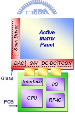
(14) Chapter 1 Introduction. 1-1. Introduction to LTPS TFT technology Nowadays, the amorphous silicon thin film transistors (a-Si TFTs) are widely used as pixel switching devices in active matrix liquid crystal displays (AMLCDs). The major advantages of a-Si TFT are low process temperature that can avoid damaging glass substrates and low leakage current that can avoid grey level shift as TFT is turned off. Fig. 1-1 shows the block diagram of active matrix display. These peripheral circuits are composed of many LSI driving circuits and connected to the panel via printed circuited board. However, as the display resolution increases, the pin number on the PCB accordingly increase, which will also lead to some problems such as complicated assembly, manufacturing cost, and yield decrease during process. Therefore, the integration of driver circuitry with display panel on the same substrate is very desirable not only to reduce the module cost but to improve the system reliability. For this reason, the polycrystalline silicon thin-film transistors (poly-Si TFTs) have attracted much attention for the system integration because of its large carrier mobility and better driving capacity. The carrier mobility of poly-Si TFT is about tens times larger than that of amorphous-silicon TFT typically below 1 cm2/V*sec. Thus, the integration of peripheral circuits in display electronics can be achieved by poly-Si TFTs, which is illustrated in Fig. 1-2. Moreover, this characteristic can let the pixel-switching elements made by smaller TFTs size, resulting in higher aperture ratio and lower parasitic gate line capacitance for the improvement of display performance. 1.
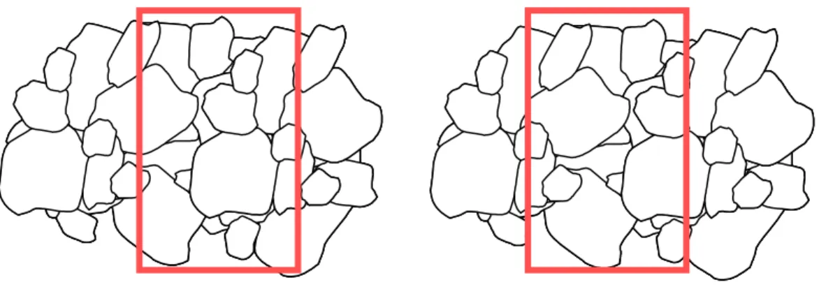
(15) In addition to flat panel displays, poly-Si TFTs have also been applied into some memory devices such as dynamic random access memories (DRAMs), static random access memories (SRAMs), electrical programming read only memories (EPROM), and electrical erasable programming read only memories (EEPROMs). Among these poly-Si technologies, low temperature polycrystalline silicon thin-film transistors (LTPS TFTs) are primarily applied on glass substrates for the display electrons since higher process temperature may cause the substrate bent and twisted. Although the advantages of LTPS TFTs are many, there are still some issues in LTPS TFTs. Examples are reliability, device variation, and well-defined model for circuit design. My thesis will focus on the device variation and well-defined model for circuit design.. 1-2. Device variation Compared with MOSFETs (Metal Oxide Semiconductor Field Effect Transistors), the LTPS TFTs are found to suffer more serious variation of their electrical parameters. The poly-Si material is a heterogeneous material made of many small Si-atoms crystals with different crystalline orientations contacting with each other. The border between small crystals is called a grain boundary which contains many disordered bonds and dangling bonds resulting in locally allowed energy states within Si band gap. Carriers trapped by these locally allowed energy states cannot contribute to conduction, which effect the formation of local depletion region and potential barrier in the grain boundary. Therefore, the electrical characteristics of LTPS TFT strongly depend on grain structure in device channel. Due to the random distribution of grain number in the channel, device performance is less controllable and the initial characteristics of LTPS TFT are different with each other, which are shown in Fig. 1-3.. 2.
(16) The device variation will result in the variation of circuit performance. Moreover, it will be reflected directly on the image performance. For the circuit integration on panel, the device variation should be taken into consideration.. 1-3. Motivation Up to now, very few works have been made on the variation issue of LTPS TFT and well-defined model for circuit simulation. Most researches about LTPS TFT aim at the improvement of the device performance. Moreover, before LTPS TFT can be widely-applied in mass production, the study of device variation and well-defined model for circuit simulation is necessary. Usually, to take device variation into consideration, simulation skill used for LTPS TFT circuits is Monte Carlo simulation with an assumption distribution. However, the simulation results of LTPS TFT circuits cannot connect to the real circuit performance. Therefore, we will focus on the real device variation distribution in this work. In chapter 2, the variation models will be proposed and discussed in detail based on statistical study. Its purpose is to establish a reliable model to estimate precisely circuit performance influenced by the device variation. Then, the device variation models and their appliances for circuit performance will be demonstrated in chapter 3. These models will improve the accuracy of the simulation results compared with other simulation models.. 1-4. Thesis Outline Chapter 1. Introduction 1-1. Introduction to LTPS TFT technology 1-2. Device variation 3.
(17) 1-3. Motivation 1-4. Thesis outline Chapter 2. Statistical analysis of TFT device parameters 2-1. Introduction to crosstie TFTs 2-2. Device fabrication and parameter extraction 2-2-1. Device fabrication 2-2-2. Parameter extraction 2-3. N-type TFT & P-type TFT 2-3-1. Initial parameter distribution 2-3-2. The distribution of initial parameter difference with different device distance 2-3-3. The models of distributions 2-4. The distribution comparison between N-type TFT and P-type TFT Chapter 3. Effects of device distribution on circuit simulation 3-1. Introduction to the differential pair and current mirror 3-2. Evaluation of the circuit performance with proposed models 3-3. Discussion and conclusion Chapter 4. Conclusion and future work References Figure captions. 4.
(18) Chapter 2 Statistical analysis of crosstie TFT device parameters. 2-1. Introduction to crosstie TFTs In previous studies, it is known that LTPS TFTs are found to suffer serious device variation even under well-controlled process. Since device variation will directly affect the circuit performance and reliability prediction, it is essential to understand where the variation may come and how the behavior variation could be. Due to the low process temperature, LTPS TFTs have different processes from IC industry. Besides, LTPS TFTs have less controllable defect number and distribution in the channel film. These may be the sources of device variation. In MOSFETs (Metal Oxide Semiconductor Field Effect Transistors), device variation sources can be divided into micro variations characterized by short correlation distances and macro variations characterized by long correlation distances, where the correlation distance is defined as the distance in which a process disturbance affects the device performance. Generally, for LTPS TFTs, macro variations usually come from the issues of process control, including gate insulator thickness LDD length fluctuation and ion implantation uniformity; micro variations come from the difference of the defect site, defect density in the active region and the activation efficiency. If the distance between mutual devices is lower than the correlation distance, the disturbance consists of micro variations and affects few devices (e.g. a charge trapped in the gate oxide layer). On the other hand, if mutual device distance is longer than this correlation distance, the disturbance composed of micro variations and macro variations affects all the devices within a defined region. Therefore, the devices. 5.
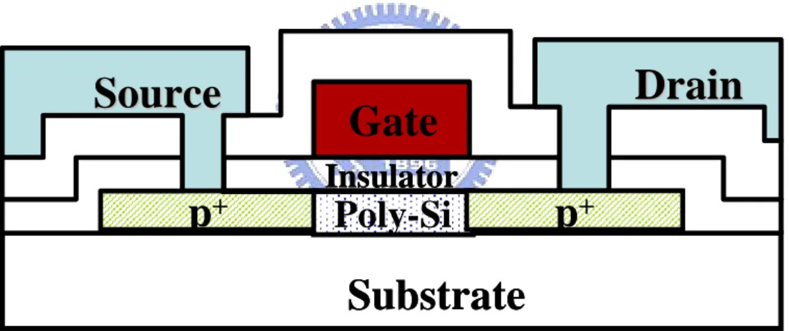
(19) placed at longer distance suffer more serious variation than devices placed close to each other. In order to study the relationship between uniformity issue and device distance, a special layout of the devices adopted in this work is shown in Fig. 2-1. The red, blue and yellow regions respectively represent the polysilicon film, the gate metal and the source/drain metal. The structure of the poly-Si film and the gate metal are in the order that resembles the crosstie of the railroad and therefore this layout is called the crosstie type layout of LTPS TFTs. The distance of mutual device is equally-spaced 40µm. In this small distance, the macro variation may be ignored and the variation of device behavior can therefore be reduced to only micro variation. So we can find out the relationship between the variation behaviors and the distance of mutual device by adopting the crosstie layout TFTs.. 2-2. Device fabrication and parameter extraction 2-2-1Device fabrication The process flow of fabricating LTPS TFTs is described as follows. Firstly, the buffer oxide and a-Si:H films were deposited on glass substrates; then XeCl excimer laser was used to crystallize the a-Si:H film, followed by poly-Si active area definition. Subsequently, a gate insulator was deposited. Then, the metal gate formation and source/drain doping were performed. A lightly doped drain (LDD) structure was used on the n-type TFTs. Dopant activation and hydrogenation were carried out after interlayer deposition. Finally, contact holes formation and metallization were performed to complete the fabrication work. The Fig. 2-2 and Fig. 2-3 show respectively the schematic cross-section structure of the N-type TFT and P-type TFT.. 2-2-2. Parameter extraction 6.
(20) Determination of the threshold voltage In most of the researches on TFT, the constant current method is widely-adopted to determine the threshold voltage (Vth). In this work, the threshold voltage is determined from this method, which extracts Vth from the gate voltage at the normalized drain current I N =I D /(Weff /Leff )=10nA for VD=0.1V. Determination of the subthreshold swing The subthreshold swing S.S (V/dec) is a typical parameter to describe the gate control ability toward channel. The subthreshold swing should be independent of drain voltage and gate voltage. In reality, it might be affected by serial resistance, short channel effect and interface traps. In our thesis, it is defined as the minimum value of the gate voltage required to increase drain current by one order of magnitude for VD = 0.1V.. ⎡ ∂ ( log I ds ) ⎤ S.S = ⎢ ⎥ ⎣⎢ ∂Vgs ⎦⎥. -1. (2-1). Determination of the field-effect mobility The field effect mobility (µFE) is derived from the transconductance gm at low drain voltage. Since the transfer characteristics of poly-Si TFTs are similar to those of conventional MOSFETs, the first order I-V relation in the bulk Si can be applied to the poly-Si TFTs, which can be expressed as. I D = µ FE Cox. W 1 [(VG − Vth )VD − VD 2 ] L 2. (2-2). Where Cox is the gate oxide capacitance per unit area, W is channel width, L is channel length and Vth is the threshold voltage.. If the drain voltage VD is much smaller compared with ( VG − Vth ), then the drain 7.
(21) current can be approximated as: I D = µ FE Cox. W (VG − VTH )VD L. (2-3). And the transconductance is defined as:. gm =. ∂I D ∂VG. VD = const .. =. WC ox µ FE VD L. Therefore, the field effect mobility can be expressed as:. µ FE =. L gm C oxW V D. (2-4). In this thesis, we extract the field-effect mobility by taking the maximum value of the gm into (2-3) when VD = 0.1V.. 2-3. N-type TFT & P-type TFT 2-3-1. Initial parameter distribution Before the following analysis, the statistical expressions, average value and standard variation are introduced. The average value AVG, X , is defined as n. ∑x. X = i=1 n. where x is the observe value.. (2-5). The standard deviation value STD, σ, is usually used to investigate the distribution of the observed value. The standard deviation value is given as. σ≡. 2 1 x− X) ( ∑ n n. ( 2-6). where x is the observe value and X is the average value. In order to obtain the more accurate parameter distributions of crosstie layout TFTs, large amount of TFT devices parameters are required. More than 1600 devices of N-type and P-type TFTs are measured and taken into statistical analysis in this 8.
(22) work. The threshold voltage (Vth), mobility (Mu), and subthreshold swing (S.S) distributions of N-type TFT are shown respctively in Fig. 2-4(a), Fig. 2-4(b) and Fig. 2-4(c) and those of P-type are shown in Fig. 2-5(a), Fig. 2-5(b) and Fig. 2-5(c). Table2-1 is the average values and standard deviation values of these initial parameter. N-type. Vth(V). Mu(cm^2/Vs). SS(V/dec). AVG. 1.69. 59.66. 0.241. STD. 0.03. 7.84. 0.0083. P-type. Vth(V). Mu(cm^2/Vs). SS(V/dec). AVG. 2.41. 75.31. 0.253. STD. 0.05. 2.29. 0.0022. Table2-1 The average values and standrad deviation values of device parameters.. These figures show the variation behaviors in different parameters of LTPS TFTs. The Vth distrubtion of N-type TFT reveals the slight left-skewed property and the sharper peak compared with the Gaussian distribution. The Mu distribution of N-type TFT is apparently asymmetric and incisive in its peak. This phenomena indicates that field effect mobility exhibits severe non-uniformity behavior compared with threshold voltage. Then, the distribution S.S of N-type TFT follows the Gussian distribution. As for the Vth and Mu distributions of P-type TFT, both of them are similar to the Gussain distribution. The P-type TFT SS distribution shows two peak and asymmetric distribution. In conclusions, some of these parameter distributions are diverse and cannot be explained. Although several studies have been made on the relationship between the grain boundaries in channel and threshold voltage and field effect mobility [1-3], there seems to be no well-established theory to explain. Therefore, if we want to find the variation behaviors with respect to the distance, it can not just. 9.
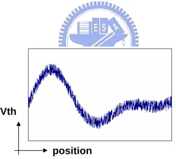
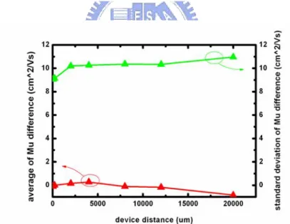
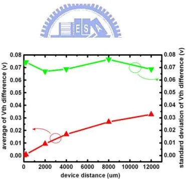
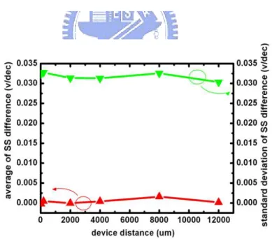
(23) classify them via these distributions and another grouping method should be mentioned. In the next section, it will be got the more identical distributions, which will be more useful to evaluate the variations in LTPS TFTs.. 2-3-2. The initial parameter difference distribution with different device distance Fig. 2-6 illustrates the threshold voltage distribution along the device position. We can take this graph as a part of Fig. 2-7, which is the same kind of graph but in longer distance. Analogy to the small signal analysis in the circuit theory, the macro variation just likes the range near the bias point and appears in piecewise linear form, while the micro variation can be taken as the noise. In order to identify the effects of macro and micro variation, the parameters differences of mutual devices under certain distance are divided with several groups according to the distance between two devices. In previous studies [5], the averages of parameters differences stand for macro variation of LTPS TFTs, while the standard deviation of parameter differences shows the micro variation in the devices. These figures, from Fig. 2-8(a) to Fig. 2-9(c), show the average and the standard deviation of parameters differences of N-type and P-type TFTs. As the mutual device distance increases, the deviations of these parameter differences almost do not change with the device distance. It can be explained that the micro variation will merely vary with distance as we expect. As for the macro variation, these figures show the diverse results. In the graph of Vth difference and S.S. difference, the averages are increasing with device distance. However, the average of the Mu difference is decreasing when the distance of mutual devices is increasing. Although the averages of the differences of these parameters show different behaviors, they still appear in linear form. On the other hand, the 10.
(24) effects of variation in a range are still minor than those of the micro variation under short device distance. In general, the macro variation results from the issues of process control, such as gate insulator thickness, LDD length fluctuation and ion implantation uniformity. This non-uniformity of process control will lead to the common shift for device parameters. The solution of macro variation is well-controlled in process. On the other hand, micro variation may come from the difference of the defect site, defect density in the active region and the activation efficiency. Since these conditions differ from device to device, the micro variation will lead to the random distribution of device parameters. Therefore, owing to describe the micro variation and evaluate the effects, the statistical analysis is need. Generally, the distance between devices is not too long for the layout of electric circuits, the major variation source is micro variation. To get more accurate simulation results, establishing a micro variation model is required.. 2-3-3. The models of distributions Since we know the device variation behaviors by above statistical analysis, how to apply these results to evaluate the effects of variation on the circuit performance is a topic we are interested in. Because the distance between two devices will not be too long for the layout of the circuit, the macro variation is not our concern. A better approach is to find the proper mathematical expression for the distribution of the differences of these parameters. Firstly, we introduce the coefficient of determination (R square) to evaluate the fitness of our work, which is defined as. r2 =. SSR SSE = 1− , where SST SST. SSR = ∑ ( ˆy − y )2 = ∑ Yˆ 2 = b12 ∑ X 12 + b22 ∑ X 22 + 2b1b2 ∑ X 1 X 2. 11.
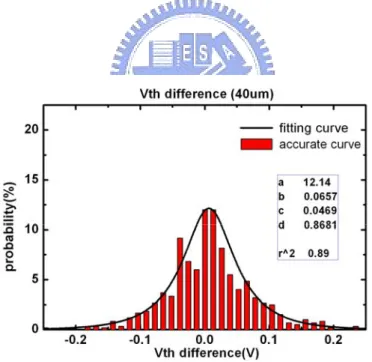
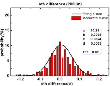
(25) SST = ∑ ( y − y )2 SSE = ∑ eˆ 2 = ∑ ( yi − ˆyi )2 Generally speaking, the values of R square above 0.7 represnent the good fitness for the chosen funcion. For the distribution of the difference of Vth, Gaussian-Lorentzian cross product is apply to the fitting, which is y=. a 2 ⎛ ⎛ 1⎛ x - b⎞ ⎞ ⎛ x - b⎞ ⎞ ⎜⎜ 1 + d ⎜ ⎟ ⎟⎟ *exp ⎜⎜ (1- d ) * ⎜ ⎟ ⎟⎟ c 2 c ⎝ ⎠ ⎝ ⎠ ⎠ ⎝ ⎠ ⎝ 2. (2-7). where a is the peak value of the distribution b is the center of the distribution c is fitting parameter related to the width of the distribution d is fitting parameter varying from 0 to 1;0 represents the pure Gaussain function ,while 1 is a pure Lorentzian distribution Fig. 2-10(a) ~ (f) are shown respcetively the Vth difference distributions of N-type and P-type TFT with different device distance. As for the distribution of the difference of Mu, the Lorentzian distribution is apply to the fitting, which is y=. a ⎛ x-b⎞ 1+ ⎜ ⎟ ⎝ c ⎠. (2-8). 2. where a is the peak value of the distribution b is the center of the distribution c is fitting parameter related to the width of the distribution. 12.
(26) The Mu difference distributions of N-type and P-type TFT with different device distance are shown in Fig. 2-11(a) ~ (f). The Gaussian function is chosen to fit the distribution of the difference of S.S, which can be expressed as. y =. a 1 x - b 2 exp( ( ) ) c 2. (2-9). where a is the peak value of the distribution b is the center (average) of the distribution c is the standard deviation of the distribution The S.S. difference distributions of N-type and P-type TFT with different device distance are shown in Fig. 2-12(a) ~ (f). The values of R squre of the above fittng curves both higher than 0.85. It clearly shows the good fitness of our proposed mathemtical model and most of the fitting parameters slightly changing with distance, which supports the effects of macro variation are minor than those of micro variation we mentioned before. The values of R squre are so high that the device micro varion behavior can be described in these proposed distribution models. Therefore, the more accurate simulation results will be obtained with these proposed models and the effects of these proposed models on circuit performance will be discussed in 3 chatper. In additon, although theses parameter difference distributions of N-type and P-type TFT can be expressed in the same mathematical function, those distributions are obvious different to some degree. The reasons of these phenomena will be discussed in next section.. 13.
(27) 2-4. The distribution comparison between N-type and P-type TFTs Fig. 2-13 and Fig. 2-14 are the distributions of Vth and SS difference of TFTs. The distributions of Vth and SS differences of N-type TFT are narrower than those of P-type TFT. This phenomena might result from channel doping of N-type TFT during process. In order to avoid obtaining the negative Vth of N-type TFT, N-type TFT should be dealt with extra process, channel doping. The extra process step might also increase an uncertain factor causing the device variation difference between N-type and P-type TFT. Fig. 2-15 is the Mu difference distributions of N-type and P-type TFT. The Mu difference distribution of N-type TFT are wider than that of P-type TFT. This phenomenon might due to the different device structure between N-type and P-type TFT. The degradation of hot-carrier effects is a serious problem and these effects are induced by the presence of intense electric fields at the drain junction. The electric field at the drain junction is determined by the ion doping and the activation process used by impurities. Therefore, the TFT with a light-doped drain (LDD) are attractive for used with N-type TFTs. However, the N-type TFT with a light-doped drain (LDD) also increases an uncertain factor causing device variation. Therefore, the Mu difference distribution of N-type TFT are wider than that of P-type TFT. Furthermore, the mathematical model for the distributions of the parameters differences is established, the applications for these models for circuit simulation will be discussed in the following chapter.. 14.
(28) Chapter 3 Effects of device distribution on circuit performance. 3-1. Introduction to the current mirror and differential pair In the design of an amplifier circuit, an essential step is the establishment of an appropriate DC operating point for the transistor. An appropriate DC operating point is characterized by a stable and predicable DC drain current Id, and a DC drain-source voltage that ensures operation in the saturation mode for all expected input signal. Therefore, a current source circuit plays an important role in design of circuits. In VLSI, a current mirror circuit is usually used as a current source because of its small area on chip and well-controlled parameters. On the other hand, coupling effect is a serious problem for signal transmission in the integrated circuit application. Fig. 3-1(a) shows that clock will couple some noise to adjacent signal line during the rising and falling time. If we transmit the input signal by two separated signal lines shown in Fig. 3-1(b), the coupling effect of clock will be cancelled by getting the difference of the signal. For this reason, the differential pairs are widely used for analog circuit design because of the immunity for the noise. However, the performance of current mirror circuits and differential pair circuits strongly depends on the match of the device. The mismatch of transistors will cause severe variation of circuit performance. In conventional CMOS, these mismatch effects can be suppressed under the well-controlled process. Compared with CMOS, LTPS TFTs suffered form more serious device variation. In order to evaluate the circuit performance of current mirror and differential pair composed of LTPS TFTs, the variation models we mentioned before can be adopted to simulate the circuit. 15.
(29) performance. The detail of circuit simulation and the comparison of other simulation skills and models will be discussed in the next section.. 3-2. Evaluation of the circuit performance with proposed models and other simulation skills In this section, a commonly-used differential pair and a current mirror circuit are used to examine the circuit performance affected by device variation. The simulation will be done by different simulation skills and models.. Current mirror Fig. 3-2 shows a basic N-type current mirror circuit. The heart of the circuit is transistor M 1 whose drain is shorted to its gate and thus is operating in the saturation region, such that I d 1 = I REF =. 1 W µ1COX ( )1 (VGS − Vt1 ) 2 2 L. (3-1). Considering transistor M 2 , it has the same VGS as M 1 , thus if we assume that it is operating in saturation, its drain current, which is the output current I O of the current source, will be IO = I D2 =. 1 W µ 2COX ( ) 2 (VGS − Vt 2 ) 2 2 L. (3-2). If the circuit is perfectly symmetric and transistor’s dimensions are equal, the output current I O and input reference current I REF will be the same. However, the transistor M 1 doesn’t match transistor M 2 in practical circuits; thus, the relationship between I O and I REF will become 16.
(30) IO I REF. ∆v ∆µ 2 µ1 (VGS − Vt1 ) 2 ( µ + 2 )(Vgs − ( vth + th 2 )) = = µ2 (VGS − Vt 2 ) 2 ( µ − ∆µ )(V − ( v − ∆vth )) 2 th 2 gs 2. (3-3). where µ is the field effective mobility Vth is the threshold voltage △µ is the field effective mobility difference of mutual devices △Vth is the threshold voltage difference of mutual devices. Differential pair with an active load Fig. 3-3 shows the N-type differential pair circuit with an active load biasing by a current mirror, and input signals, v1 and v 2 ,are applied to the gate terminal of transistor M1 and M2. In general, input signals to a differential amplifier contain a common-mode component, vcm =. v1 + v2 , and a differential-mode component, 2. vd = v1 − v2 . Then, the output signal will be given by vo = Ad vd + Acm vcm where Ad is the differential-mode gain and Acm is the common-mode gain [6]. For an ideal differential pair, the common-mode gain is zero because the circuit is perfectly symmetric. Nevertheless, the transistors in practical circuits are asymmetric with the result that the common-mode gain will not be zero. The common-mode gain can be written as (g − g m 4 ) 2 µV gs − ( ∆µVth + ∆Vth µ ) ∆Vout ACM = ≅ m3 = 2 µ (V − V ) ( g m3 + g m4 ) ∆Vin.CM gs th. where µ is field effective mobility Vth is the threshold voltage 17. (3-4).
(31) △µ is the field effective mobility difference of mutual devices △Vth is the threshold voltage difference of mutual devices. Therefore, we can take the common-mode gain and the ratio of I O and I REF as indices for our simulation target to evaluate the device variation effect. Before the simulation, it is essential to transform the distribution into the corresponding values for Monte Carlo simulation. Take the distribution consisting of four variables as example, as shown in Fig. 3-4. Based on the probability in Fig. 3-4, a table of range mapping can be established, as shown in Fig. 3-5. For a series of uniformly random values in the range from 0 to 1 generated by the computer, the corresponding series can be obtained by looking up table 1. Thus, the distribution of the looked-up values match that shown in Fig. 3-5. Similarly, the distributions of Vth difference and Mu difference can be generated. In order to get the stable and reliable simulation results, 210,000 times of data transformation for each distribution were executed. To compare the effects of device variation on the circuit performance, two distribution models are adopted in the Monte Carlo simulation. One is the proposed model mentioned in chapter 2 and the other is the Gaussian distribution. The parameters of Gaussian distribution used here correspond to the mean value and the deviation of parameter difference data. Fig. 3-6(a), Fig. 3-6(b), Fig. 3-7(a) and Fig 3-7(b) are the device parameter difference distributions for circuit simulation conditions. Monte Carlo method with Gaussian distribution and our proposed model are represented by red line and black line individually.. 3-3. Discussion and conclusion The simulation results of current mirror circuit and differential pair circuit are. 18.
(32) shown in Fig. 3-8(a), Fig. 3-8(b), Fig. 3-9(a) and Fig. 3-9(b), respectively. The results of Monte Carlo method with Gaussian distribution and our proposed model which is also real data distribution are represented by red line and black line individually. From Fig. 3-9(a) and Fig 3-9(b), it can be observed that the simulation results of current mirror circuit and differential pair circuit of P-type using Monte Carlo analysis with Gaussian distribution are almost the same as the results using our proposed model. On the other hand, the simulation results of N-type current mirror and differential pair circuit using Monte Carlo method with Gaussian distribution are different to the results using our proposed model. Namely, Monte Carlo analysis with Gaussian distribution can be used as the distributions of parameter difference for P-type TFT, but it cannot be used as the parameter difference distributions for N-type TFT. It can also be observed that simulation using Gaussian distribution will underestimate the N-type circuit performance. Generally, Monte Carlo analysis used in most simulation tools doesn’t support Lorentzian and Gaussian Lorentzian profiles for circuit simulation. Moreover, the major reason making the simulation results of N-type circuits difference between Gaussian distribution and our proposed model distribution is the distribution of Mu difference. From the Fig. 2-15, it can be found that the Mu difference distribution of N-type TFT is a little wider than that of P-type TFT. So the standard deviation value of Mu differences of N-type TFT is bigger than that of P-type TFT. Therefore, the Gaussian distribution defined by the average value and standard deviation of the Mu differences of N-type TFT is much wider than the real Mu difference distribution of N-type TFT. However, the concentration degree of the Mu difference distributions of N-type TFT and P-type TFT are almost the same. Accordingly, the Gaussian distribution might be defined by the inter-quartile range of the Mu difference data of N-type TFT instead of the standard deviation. From Fig.3-10(a) the Gaussian 19.
(33) distribution which is defined by inter-quartile range of the Mu difference data of N-type TFT has a better fitness for the Mu difference distribution of N-type TFT. In the same way, let other distributions be described as the Gaussian profile defined by inter-quartile region of parameter differences again. They are shown in Fig. 3-10(a) ~ (d), respectively. From these graphs, the Gaussian distributions defined by inter-quartile region are all similar to real distribution which is our proposed distribution. And the circuit simulation results using the Gaussian distribution defined by the inter-quartile range can be obtained in Fig. 3-11(a) ~ (d). It can also be found that the simulation results are almost the same with those using our proposed model. In conclusion, if the inter-quartile range of the parameter differences data is used for the definition of Gaussian distribution, the parameter difference distribution described as Gaussian profile or Lorentzian profile is almost the same. Therefore, Monte Carlo analysis with Gaussian distribution still can be used to simulate LTPS TFT circuits in simulation tool and the more accurate circuit simulation results can be obtained than before.. 20.
(34) Chapter 4 Conclusion In this thesis, the variation characteristics of LTPS TFTs are statistically investigated. In order to study the respective effects of micro and macro variation, a special layout of TFTs called “crosstie” is adopted in this work. By introducing this special layout of TFTs, the dependence of distance for device variations can be found. In chapter two, we classify two kinds of variation behaviors by grouping the difference of parameters in TFTs under different device distances. It can be observed that the variation in the range will be piecewise linear and the micro variation will be invariant in device position. The following is the proposed models for the difference of parameters. In this model, it can be observed that the shape of these distributions seems to be no changes with different device distances. This result tells us the micro variation will be invariant in device position indeed. The following is the application for these models we proposed. The simulations of the mismatch due to the device variation in differential pair circuit and current mirror circuit are demonstrated. The simulation results of N-type circuits using Gaussian distribution defined by the average value and standard deviation of parameters difference are different to results by using our proposed models. It was also found that Gaussian model commonly assumed might underestimate the circuit performance. On the contrary, the simulation results of P-type circuits are almost similar to the results using our proposed models. However, the concentration degree of the Mu difference distributions of N-type and P-type is almost the same. Another way to describe Gaussian distribution is proposed. The Gaussian distributions defined by the inter-quartile range of parameters difference data have a good fitness for the. 21.
(35) real data distribution compared with Gaussian distribution defined by the standard deviation. Therefore, the inter-quartile region of parameters difference is a major factor to decide the profile of these distributions and Monte Carlo analysis with Gaussian distribution still can be used to simulate LTPS TFT circuits in simulation tools. Furthermore, the circuit simulation results will be more accurate than before.. 22.
(36) References [1] Cheng-Ho Yu, “Study of Reliability Variation for Low Temperature Polysilicon Thin Film Transistors”, Diss. National Chiao Tung University, p. 69, 2005. [2] Kitahara, Yoshiyuki; Toriyama, Shuichi; Sano, Nobuyuki, “A new grain boundary model for drift-diffusion device simulations in polycrystalline silicon thin-film transistors”, Japanese Journal of Applied Physics, Part 2: Letters, v 42, n 6 B, p. L634-L636, 2003. [3] Wang, Albert W., Saraswat, Krishna C., “Modeling of grain size variation effects in polycrystalline thin film transistors”, Technical Digest - International Electron Devices Meeting, p. 277-280, 1998. [4] Wang, Albert W. (Agilent Technologies); Saraswat, Krishna C., “Strategy for modeling of variations due to grain size in polycrystalline thin-film transistors”, IEEE Transactions on Electron Devices, v 47, n 5 , p. 1035-1043, 2000. [5] Shi-Zhe Huang, “Statistical Study on the Uniformity Issue of Low Temperature Polycrystalline Silicon Thin Film Transistor”, Diss. National Chiao Tung University, p. 14, 2005. [6] Razavi, “Design of analog integrated circuit”, p. 121, 2001.. 23.
(37) Fig. 1-1 The block diagram of an active matrix display. Fig. 1-2 The integration of peripheral circuits in a display achieved by poly-Si TFTs. 24.
(38) Fig. 1-3 The initial characteristics of LTPS TFTs are different from one another due to various distributions of grain boundaries. Fig. 2-1 The layout of the crosstie TFTs. 25.
(39) Source. Drain. Gate Insulator. n+. n-. Poly-Si n-. n+. Substrate Fig. 2-2 The schematic cross-section structure of the N-type poly-Si TFT with lightly doped drain. Source p+. Drain. Gate Insulator. Poly-Si. p+. Substrate Fig. 2-3 The schematic cross-section structure of the P-type poly-Si TFT. 26.
(40) Fig. 2-4 (a) The distributions of threshold voltage for N-type TFTs. Fig. 2-4 (b)The distributions of mobility for N-type TFTs. 27.
(41) Fig. 2-4 (c)The distributions of subthreshold for N-type TFTs. Fig. 2-5 (a)The distributions of threshold voltage for P-type TFTs. 28.
(42) Fig. 2-5 (b)The distributions of mobility for P-type TFTs. Fig. 2-5 (c)The distributions of subthreshold for P-type TFTs. 29.
(43) Fig. 2-6 The threshold voltage distribution along the device position. Vth. position Fig. 2-7 Simulation of the threshold voltage distribution along the device position for a long range. 30.
(44) Fig. 2-8 (a) The average and the standard deviation of the threshold voltage differences of N-type TFTs. Fig. 2-8 (b) The average and the standard deviation of the mobility differences of N-type TFTs. 31.
(45) Fig. 2-8 (c) The average and the standard deviation of the subthreshold swing differences of N-type TFTs. Fig. 2-9 (a) The average and the standard deviation of the threshold voltage differences of P-type TFTs. 32.
(46) Fig. 2-9 (b) The average and the standard deviation of the mobility differences of P-type TFTs. Fig. 2-9 (c) The average and the standard deviation of the subthreshold swing differences of N-type TFTs. 33.
(47) Fig. 2-10 (a) The distribution of Vth difference of N-type TFT and its fitting curve under the device distance of 40 µm. Fig. 2-10 (b) The distribution of Vth difference of N-type TFT and its fitting curve under the device distance of 200 µm. 34.
(48) Fig. 2-10 (c) The distribution of Vth difference of N-type TFT and its fitting curve under the device distance of 2000 µm. Fig. 2-10 (d) The distribution of Vth difference of P-type TFT and its fitting curve under the device distance of 40 µm. 35.
(49) Fig. 2-10 (e) The distribution of Vth difference of P-type TFT and its fitting curve under the device distance of 200 µm. Fig. 2-10 (f) The distribution of Vth difference of P-type TFT and its fitting curve under the device distance of 2000 µm. 36.
(50) Fig. 2-11 (a) The distribution of mobility difference of N-type TFT and its fitting curve under the device distance of 40 µm. Fig. 2-11 (b) The distribution of mobility difference of N-type TFT and its fitting curve under the device distance of 200 µm. 37.
(51) Fig. 2-11 (c) The distribution of mobility difference of N-type TFT and its fitting curve under the device distance of 2000 µm. Fig. 2-11 (d) The distribution of mobility difference of P-type TFT and its fitting curve under the device distance of 40 µm. 38.
(52) Fig. 2-11 (e) The distribution of mobility difference of P-type TFT and its fitting curve under the device distance of 200 µm. Fig. 2-11 (f) The distribution of mobility difference of P-type TFT and its fitting curve under the device distance of 2000 µm. 39.
(53) Fig. 2-12 (a) The distribution of S.S difference of N-type TFT and its fitting curve under the device distance of 40 µm. Fig. 2-12 (b) The distribution of S.S difference of N-type TFT and its fitting curve under the device distance of 200 µm. 40.
(54) Fig. 2-12 (c) The distribution of S.S difference of N-type TFT and its fitting curve under the device distance of 2000 µm. Fig. 2-12 (d) The distribution of S.S difference of P-type TFT and its fitting curve under the device distance of 40 µm. 41.
(55) Fig. 2-12 (e) The distribution of S.S difference of P-type TFT and its fitting curve under the device distance of 200 µm. Fig. 2-12 (f) The distribution of S.S difference of P-type TFT and its fitting curve under the device distance of 2000 µm. 42.
(56) Fig. 2-13 The distributions of Vth difference of N-type and P-type TFTs. Fig. 2-14 The distributions of SS difference of N-type and P-type TFTs. 43.
(57) Fig. 2-15 The distributions of Mu difference of N-type and P-type TFTs. Fig. 3-1 (a) The coupling effects of the clock signal. 44.
(58) Fig. 3-1 (b) The signal transmission is done by differential signal. IREF M1. Io M2. Fig. 3-2 A basic N-type current mirror circuit structure. 45.
(59) VDD M5. M6. IREF. Vout. V in,CM M1. M3 M2. M4. V in,CM. Fig. 3-3 The N-type differential pair circuit with an active load biasing by a current mirror. Fig. 3-4 Simple distribution with four variables. 46.
(60) Fig. 3-5 The table for data transformation. Fig. 3-6 (a) The Gaussian distribution defined by the average and standard deviation of Vth differences of N-type TFTs and our proposed model distribution. 47.
(61) Fig. 3-6 (b) The Gaussian distribution defined by the average and standard deviation of Mu differences of N-type TFTs and our proposed model distribution. Fig. 3-7 (a) The Gaussian distribution defined by the average and standard deviation of Vth differences of P-type TFTs and our proposed model distribution. 48.
(62) Fig. 3-7 (b) The Gaussian distribution defined by the average and standard deviation of Mu differences of P-type TFTs and our proposed model distribution. Fig. 3-8 (a) The simulation results of N-type current mirror circuit. 49.
(63) Fig. 3-8 (b) The simulation results of N-type differential pair circuit. Fig. 3-9 (a) The simulation results of P-type current mirror circuit. 50.
(64) Fig. 3-9 (b) The simulation results of P-type differential pair circuit. Fig. 3-10 (a) The Gaussian distribution defined by the inter-quartile range of Vth differences of N-type TFTs and our proposed model distribution. 51.
(65) Fig. 3-10 (b) The Gaussian distribution defined by the inter-quartile range of Mu differences of N-type TFTs and our proposed model distribution. Fig. 3-10 (c) The Gaussian distribution defined by the inter-quartile range of Vth differences of P-type TFTs and our proposed model. 52.
(66) Fig. 3-10 (d) The Gaussian distribution defined by the inter-quartile range of Mu differences of P-type TFTs and our proposed model distribution. Fig. 3-11 (a) The simulation results of N-type current mirror circuit. 53.
(67) Fig. 3-11 (b) The simulation results of N-type differential pair circuit. Fig. 3-11 (c) The simulation results of P-type current mirror circuit. 54.
(68) Fig. 3-11 (d) The simulation results of P-type differential pair circuit. 55.
(69) 學 經 歷. 姓 名:彭 國 烽 性 別:男 生 日:民國七十一年三月三十一日. 學 經 歷:國立台灣海洋大學電機工程學系 國立交通大學光電工程研究所碩士班. (89.9 ~ 93.6) (93.9 ~ 95.6). 碩士班論文題目: 低溫多晶矽薄膜電晶體元件特性分布用於電路模擬之研究 (Study on the Characteristics Distributions of LPTS TFTs for Circuit Simulation). 56.
(70)
數據
+7

相關文件
在1980年代,非晶矽是唯一商業化的薄膜型太 陽能電池材料。非晶矽的優點在於對於可見光
If the bootstrap distribution of a statistic shows a normal shape and small bias, we can get a confidence interval for the parameter by using the boot- strap standard error and
Comparison of B2 auto with B2 150 x B1 100 constrains signal frequency dependence, independent of foreground projections If dust, expect little cross-correlation. If
In this paper we establish, by using the obtained second-order calculations and the recent results of [23], complete characterizations of full and tilt stability for locally
In this paper we establish, by using the obtained second-order calculations and the recent results of [25], complete characterizations of full and tilt stability for locally
◦ Lack of fit of the data regarding the posterior predictive distribution can be measured by the tail-area probability, or p-value of the test quantity. ◦ It is commonly computed
雙極性接面電晶體(bipolar junction transistor, BJT) 場效電晶體(field effect transistor, FET).
1INTRODUCTION DuyMinhDang ChristinaC.Christara Adaptiveandhigh-ordermethodsforvaluingAmericanoptions
Furthermore, by comparing the results of the European and American pricing prob- lems, we note that the accuracies of the adaptive finite difference, adaptive QSC and nonuniform
