Structural and electrical investigation of laser annealed ( Pb , Sr ) Ti O 3 thin films
Jyh-Liang Wang, Yi-Sheng Lai, Sz-Chian Liou, Bi-Shiou Chiou, Chueh-Kuei Jan, and Huang-Chung Cheng
Citation: Journal of Vacuum Science & Technology B 26, 41 (2008); doi: 10.1116/1.2819255 View online: http://dx.doi.org/10.1116/1.2819255
View Table of Contents: http://scitation.aip.org/content/avs/journal/jvstb/26/1?ver=pdfcov Published by the AVS: Science & Technology of Materials, Interfaces, and Processing
Articles you may be interested in
Reduced leakage current in BiFeO 3 thin films with rectifying contacts Appl. Phys. Lett. 98, 232901 (2011); 10.1063/1.3597794
Leakage current behavior in lead-free ferroelectric ( K , Na ) NbO 3 -LiTaO 3 -LiSbO 3 thin films Appl. Phys. Lett. 97, 262902 (2010); 10.1063/1.3531575
Structural, electrical, and magnetic properties of multiferroic Bi 1 x La x Fe 1 y Co y O 3 thin films J. Appl. Phys. 107, 124109 (2010); 10.1063/1.3437232
Ferroelectric properties and leakage current characteristics of radio-frequency-sputtered SrBi 2 ( V 0.1 Nb 0.9 ) 2 O 9 thin films
J. Appl. Phys. 96, 2181 (2004); 10.1063/1.1766096
Electrical properties of chemical-solution-derived Bi 3.54 Nd 0.46 Ti 3 O 12 ferroelectric thin films J. Appl. Phys. 94, 7376 (2003); 10.1063/1.1622777
„Pb,Sr…TiO
3thin films
Jyh-Liang Wang
Department of Electronics Engineering and Institute of Electronics, National Chiao Tung University, 1001 Ta Hsueh Rd., Hsinchu 30050, Taiwan
Yi-Sheng Laia兲
Department of Materials Science and Engineering, National United University, Miaoli 36003, Taiwan
Sz-Chian Liou
Center for Condensed Matter Sciences, National Taiwan University, Taipei 10617, Taiwan
Bi-Shiou Chiou, Chueh-Kuei Jan, and Huang-Chung Cheng
Department of Electronics Engineering and Institute of Electronics, National Chiao Tung University, 1001 Ta Hsueh Rd., Hsinchu 30050, Taiwan
共Received 16 July 2007; accepted 5 November 2007; published 2 January 2008兲
Material and electrical characteristics of共Pb,Sr兲TiO3共PSrT兲 films irradiated by various laser pulses
and laser fluences are investigated in this work. Enhanced crystallinity can be obtained after excimer laser annealing 共ELA兲. However, grain growth induced by ELA is nonuniform, and the effect is limited to the upper region of the films. As the number of laser pulses increases to 120, the film shows stronger diffraction intensities and increased oxygen content, resulting in a distinct capacitance versus electric field hysteresis loop and a larger dielectric constant than the nonirradiated one. The leakage current is found to be associated with the interface quality. The conduction mechanism of nonirradiated and irradiated PSrT films is mainly governed by Schottky emission at low electric fields, whereas the Poole-Frenkel emission occurs for films irradiated with more than 120 laser pulses or laser fluences larger than 90.5 mJ/cm2at high electric fields. © 2008
American Vacuum Society. 关DOI: 10.1116/1.2819255兴
I. INTRODUCTION
共Pb,Sr兲TiO3共PSrT兲 films, with perovskite structure, have
received much attention lately due to their potential applica-tions in memory, sensor, and microwave devices.1–6 The PSrT film constitutes a solid solution of PbTiO3共PTO兲 and
SrTiO3 共STO兲. PTO exhibits ferroelectric transition at the
Curie temperature of 490 ° C, whereas STO exhibits no ferroelectric phase transition, but undergoes structural phase transition from cubic to tetragonal symmetry around −168 ° C共105 K兲.7Therefore, PTO and STO films, at room temperature, have tetragonal and cubic structures, respec-tively. As a result, control of the crystallization temperature and dielectric properties can be realized by modulating the Pb and Sr content in the PSrT solid solution.1,2
Ferroelectric thin films mostly require low-temperature processes for integrated-circuit and microelectromechanical systems applications to prevent thermal damage of previ-ously fabricated structure. Nevertheless, deposition of ferro-electric lead-titanate films, such as PTO and Pb共Zr,Ti兲O3
共PZT兲, are usually conducted at high temperatures 共⬎600 °C兲 to achieve good crystallinity of a perovskite structure.8 The high-temperature 共⬎490 °C兲 process results in volatilizing lead oxide共Pb–O compounds兲 in lead-titanate-based thin films,9,10 which in turn affects the film composi-tion and degrades the electrical properties of the ferroelectric
device. Thus, a low-temperature process with short thermal duration is certainly required for the deposition of PSrT thin films.
In this work, PSrT films were prepared on a
Pt/Ti/SiO2/Si substrate at 200 °C using the pulsed-laser
deposition 共PLD兲 technique, and then the films were sub-jected to excimer laser annealing 共ELA兲. The major advan-tages of the ELA technique are the formation of large grains with excellent structural quality and the ability to process selected areas. The noble metal platinum共Pt兲 is used as the electrode of the Pt/PSrT/Pt capacitor because of its low power consumption and low resistive capacitive delay,6 com-pared to the conductive oxide.9 The ELA technique can achieve local high-temperature heating within a very short duration, which has been applied in forming ultrashallow junctions11 and producing low-temperature polysilicon thin-film transistors.12–16 Some studies of the properties of PZT and共Ba,Sr兲TiO3共BST兲 films post-treated by ELA have been
reported.17–21 However, the accumulated laser energy on physical/electrical properties of PSrT films has not been ad-dressed much. Therefore, this study will investigate the ef-fect of accumulated laser energy on the relationship between the structural and electrical characteristics of low-temperature-deposited共300 °C兲 PSrT films.
II. EXPERIMENTAL PROCEDURES
A multilayer of Pt/PSrT/Pt/Ti/SiO2/p-type Si was used
to simulate the structure of a capacitor over a bit line. The a兲Electronic mail: [email protected]
Pt/Ti films of 100/4 nm were sputtered onto the SiO2/Si as the bottom electrode/adhesion layer. PSrT films 120 nm thick were deposited by a KrF pulsed-laser deposition共PLD兲
system 共LPX 210i, Lambda Physik, =248 nm, pulse
width= 25 ns兲. A set of optical lenses was used to focus the excimer laser beam onto the共Pb0.6, Sr0.4兲TiO3 target. In the process of PLD PSrT film deposition, the target-to-substrate distance was 4 cm. The deposition temperature and oxygen pressure were 200 ° C and 80 mTorr, respectively. The laser pulse rate and average laser fluence were 5 Hz and 1.55 J/cm2per pulse, respectively.
The position of the optical lens was changed in order to enlarge the irradiated area for laser annealing. The as-deposited PLD PSrT thin films were then postirradiated by the KrF excimer laser. The number of laser pulses was 60, 120, and 180. The laser fluence was controlled at
47.6 mJ/cm2 per pulse. To study the effect of the laser flu-ence, the number of laser pulses was kept at 40 pulses. The laser fluences are 66.7, 90.5, and 105.6 mJ/cm2. The
sub-strate temperature was 300 ° C, which was calibrated at the wafer upper surface. Marmorstein et al. indicated that sub-strate heating would decrease the cooling rate of the tem-perature gradient induced by ELA, which would enhance the grain growth of ferroelectric films.12 The oxygen pressure was fixed at 80 mTorr during the ELA process. The laser fluences were calibrated inside the vacuum chamber by a pyroelectric power meter.
The surface roughness of PSrT films was examined by atomic force microscopy共AFM兲 共DI Nano-Scope III, Digital Instruments兲. The stoichiometry of PSrT films was character-ized by x-ray photoelectron spectroscopy关ESCA 210, Fison 共VG兲兴. The crystallinity of the film was analyzed by glancing-incident-angle x-ray diffraction 共GIAXRD兲 共D/MAX2500, Rigaku, using Cu K␣, ⬃0.154 nm兲 with a fixed incident angle of 2°. Cross-sectional transmission elec-tron microscopy 共TEM兲 samples were prepared by standard sample preparation techniques with tripod polishing and ion milling using the Gatan PIPS system operated at 3 kV. The TEM experiments were carried out on a JEM-2000FX 共JEOL Ltd.兲 operated at 200 keV.
After the physical characterization, the Pt top electrodes, with a diameter of 165m, were deposited by sputtering and
TABLEI. Summarized material properties of PLD PSrT films nonirradiated and postexcimer laser annealed共post-ELA兲 at laser fluence of 47.6 mJ/cm2
per pulse with various laser pulses.
Nonirradiated
Number of post-ELA pulse 60 120 180 rms surface roughness Rrms共nm兲a 0.5 6.2 8.5 7.1 I100 共100兲-oriented intensityb 0 0 304 99 I110 共110兲-oriented intensityb 0 82 1081 392 Pb/共Pb+Sr兲 lead elemental ratioc
0.37 0.39 0.41 0.41
Sr/共Pb+Sr兲
strontium elemental ratioc
0.63 0.61 0.59 0.59
Ti/共Pb+Sr兲
titanium elemental ratioc
1.11 1.16 1.11 1.14
O/共Pb+Sr兲
oxygen elemental ratioc
2.83 2.84 2.89 3.07
aEvaluated from AFM analysis. bEvaluated from GIAXRD pattern. cEvaluated from ESCA analysis.
FIG. 1. Glancing-incident-angle x-ray diffraction 共GIAXRD兲 patterns for PSrT films共a兲 nonirradiated and post-ELA with 共b兲 60, 共c兲 120, and 共d兲 180 pulses.
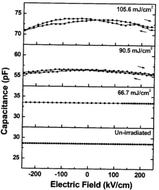
FIG. 2.关共a兲–共d兲兴 AFM images and 共e兲 surface roughness of PLD PSrT films nonirradiated and postexcimer laser annealed共ELA兲 at various laser flu-ences:共a兲 nonirradiated, 共b兲 66.7, 共c兲 90.5, and 共d兲 105.6 mJ/cm2.
42 Wang et al.: Structural and electrical investigation of thin films 42
were then patterned by the shadow-mask process. Next, the voltage was biased on the top electrode, and the bottom elec-trode was grounded. The combination of a semiconductor parameter analyzer 共4156C, Agilent Technologies兲 and a probe station was used to measure the current-voltage 共I-V兲 characteristics. A capacitance-voltage共C-V兲 analyzer 共Pack-age 82 system C-V 590, Keithley兲 was also used to measure
C-V curves at 100 kHz.
III. RESULTS AND DISCUSSION
To probe into the effects of ELA on PSrT films, the as-deposited sample was treated by mock-ELA with zero laser pulse共nonirradiated兲 to study the influence of substrate heat-ing durheat-ing the ELA process. Table I summarizes the physical
properties of PLD PSrT films nonirradiated and postexcimer laser annealed共post-ELA兲 with various laser pulses. It can be seen that the minimum normalized root-mean-square rough-ness共Rrms兲 and maximum Rrmsare 0.5 and 8.5 nm for films
nonirradiated and post-ELA with 120 pulses, respectively. The Rrms further decreases as the number of laser pulses
increases. Figure 1 shows the GIAXRD pattern of PSrT films as a function of laser pulses. The nonferroelectric pyrochlore phase is not observed from the GIAXRD pattern. The GI-AXRD pattern presents the crystallinity of the upper region of PSrT films and indicates diffraction intensities of 共100兲 and 共110兲 orientations, which may be associated with the accumulated laser energy.15,16 Table I also shows that the ratio of O to 共Pb+Sr兲 关denoted by O/共Pb+Sr兲兴 varies from 2.83 to 3.07 as the laser pulse increases. In contrast, the laser pulse seems to have little influence on the value of Pb/共Pb + Sr兲, Sr/共Pb+Sr兲, and Ti/共Pb+Sr兲. We infer that the oxygen deficiency on the surface of the films can be eliminated by increasing the total number of laser pulses. In short, these results suggest that the surface roughness, oxygen content, and crystallinity of the upper region of PSrT films could apparently be affected by increasing the number of laser pulses during ELA.
On the other hand, Fig. 2 shows AFM images of PSrT films before and after irradiation at various laser fluences. One can see that the surface roughness increases at first and then decreases as the laser fluence increases. In comparison, the surface roughness shows a similar trend to that of PSrT films irradiated with an increasing number of laser pulses.
FIG. 3. Cross-sectional TEM images and selected-area diffraction patterns 共SADPs兲 of PSrT films nonirradiated and post-ELA at laser energy fluence of 47.6 mJ/cm2per pulse with 180 pulses:共a兲 bright-field image and SADP
of nonirradiated samples,共b兲 bright-field image and dark-field image 共inset兲 of post-ELA samples, and共c兲 enlarged BF image and SADP 共inset兲 of the square mark region.
FIG. 4. Capacitance–electric field共C-E兲 hysteresis loops of PSrT films non-irradiated and post-ELA with various laser pulses.
The decrease of surface roughness is probably due to a melt-ing state on the surface when irradiated with larger laser fluence or with more laser pulses.
Figure 3 shows the cross-sectional TEM images of PSrT films before and after irradiation with various laser pulses. The bright-field共BF兲 image of the non-irradiated PSrT film is shown in Fig. 3共a兲. Because of the lack of feature and no observed grain boundaries, we suggest that the nonirradiated PSrT film is amorphous. In addition, the corresponding selected-area diffraction pattern共SADP兲 关inset of Fig. 3共a兲兴 with the diffuse ring pattern also confirms the amorphous state of the nonirradiated PSrT film. In contrast, the post-ELA film with 180 pulses reveals an image of a large reverse-pyramid grain关circular mark region in Fig. 3共b兲兴 and numerous nanograins 2 – 5 nm in diameter, as seen in Fig. 3共b兲. The corresponding dark-field image is also shown in the inset of Fig. 3共b兲. The enlarged BF image with the square mark region in Fig. 3共b兲 is shown in Fig. 3共c兲. It clearly shows that the size of the nanograins decreases from film surface to the bottom, which suggests that most of the propa-gating laser energy is absorbed within the upper region of PSrT films. The corresponding SADP 关inset of Fig. 3共c兲兴 shows an intense ring pattern and indicates that the crystal-linity of films is enhanced after the ELA treatment, consis-tent with the result of GIAXRD. The results show that grain growth induced by ELA is not uniform 共i.e., from top to bottom of the film兲, and the influence of laser irradiation only works on the upper region of PSrT films. It indicates that only a few nanograins can grow into large grains, and most of the nanograins would repeat the process of coarsening, dissolving, and nucleating in each irradiation of the laser pulses, which was also observed in ELA polysilicon.15,16
Figure 4 shows the capacitance versus electric field共C-E兲 characteristics of PSrT films as a function of laser pulses. The figure presents a typical C-E hysteresis characteristic of ferroelectric materials. According to the coercive field 共Ec兲 of the hysteresis loop, the capacitance shows a maximum value at negative bias when the applied field sweeps from +200 to − 200 kV/cm. However, the maximum capacitance appears at positive Ec when the applied field sweeps in the reverse direction. It is argued that the asymmetric C-E loops may originate from the difference between the upper region and lower region of PSrT films, where the upper region is intensively impacted by ELA. The dielectric constants, evaluated from the zero-field capacitance, are 18.1, 20.7, 61.7, and 46.8 for films before and after ELA with 60, 120, and 180 pulses, respectively, which are consistent with the intensity of diffraction patterns. It indicates that the distinct
C-E hysteresis loops and larger dielectric constants can be
FIG. 5. Capacitance–electric field共C-E兲 hysteresis loops of PSrT films non-irradiated and post-ELA at various laser fluences.
FIG. 6. Schottky emission plot fitting of log共J/T2兲 vs E1/2for Pt/PSrT/Pt
capacitors under共a兲 positive bias and 共b兲 negative bias.
FIG. 7. Current density vs electric field共J-E兲 characteristics for PSrT films nonirradiated and post-ELA at various laser fluences.
44 Wang et al.: Structural and electrical investigation of thin films 44
obtained by irradiating with more laser pulses共艌120兲, which would improve the ferroelectricity of PSrT films.
Figure 5 shows the C-E characteristics of PSrT films as a function of laser fluence. The ferroelectricity appears when the laser fluence is higher than 90.5 mJ/cm2. From Figs. 4
and 5, the results suggest that the ferroelectricity is improved by more laser pulses or larger laser fluences.
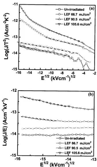
Figures 6 and 7 present the leakage current as a function of laser pulses and laser fluences. It is seen that the nonirra-diated PSrT films exhibit the lowest leakage current. PSrT films irradiated with 120 pulses show the largest leakage current. On the other hand, the largest leakage current ap-pears for films irradiated at 105.6 mJ/cm2. It seems that the
leakage current is associated with surface roughness, as shown in Table I and Fig. 2.
The conduction mechanism can be interpreted as Schottky emission 共SE兲 and Poole-Frenkel emission 共PF兲, where the trap states are related to interface-limited and bulk-limited characteristics, respectively.18,22,23If the conduction current follows SE behavior, then a log共J/T2兲 against E1/2 plot
should be linear, where T is the absolute temperature. Simi-larly, a log共J/E兲 against E1/2 plot can be made for PF.
Fig-ures 8共a兲 and 9共a兲 present the SE plot of Pt/PSrT/Pt capaci-tors as a function of laser pulses and laser fluences, respectively. The leakage currents at low electric fields are dominated by the increased interface states, which strongly depends on laser pulses and laser fluences. The magnitude of the leakage current is usually associated with the oxygen stoichiometry and interfacial properties of ferroelectric films.18,22Since the conduction characteristics of PSrT films are mainly governed by SE at lower electric fields, the leak-age current of films is most likely correlated with the inter-facial properties. It is also observed that the asymmetry of leakage currents becomes significant as the laser pulses or laser fluences increase共Figs. 6 and 7兲. Since the materials of the top and bottom electrodes are the same 共i.e., Pt兲, the increased leakage current under a negative bias can be linked to the defects at the upper electrode/film interface 共i.e., the rough interface兲.24,25Figures 8共b兲 and 9共b兲 show the PF plot
of Pt/PSrT/Pt capacitors as a function of laser pulses and laser fluences at high electric fields under negative bias. We found that the PF emission becomes the dominant conduc-tion mechanism for films irradiated with more than 120 laser
FIG. 8. Poole-Frenkel emission plot fitting of log共J/E兲 vs E1/2under nega-tive bias for PSrT films nonirradiated and post-ELA with various laser
pulses. FIG. 9. 共a兲 Schottky emission plot fitting of log共J/T2兲 vs E1/2and共b兲
Poole-Frenkle emission plot fitting of log共J/E兲 vs E1/2for PSrT films nonirradiated and post-ELA at various laser fluences.
pulses or with laser fluences larger than 90.5 mJ/cm2. It
im-plies that the deep trapping states are generated as the accu-mulated laser energy increases, which may be connected with the grain-boundary defects of the large grains induced by the ELA process共Fig. 3兲.
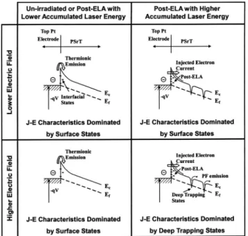
Figure 10 illustrates the electron energy band of PSrT films and shows that the interface of substrate electrodes acts as an n-type semiconductor due to the generation of oxygen vacancies in ABO3 perovskites.26 It reveals that PSrT films
non-irradiated and post-ELA with fewer laser pulses 共⬍120兲 or smaller laser fluences 共⬍90.5 mJ/cm2兲 have
smoother surfaces and fewer surface defects, yielding the lower leakage current dominated by surface states and the conduction governed by SE behavior at the applied field range. Conversely, post-ELA PSrT films with more laser pulses共艌120兲 and larger laser fluences 共艌90.5 mJ/cm2兲
ex-hibit rougher surfaces, more surface defects, and deep trap-ping states inside films, yielding larger leakage currents. For post-ELA PSrT films with larger accumulated laser energy, the low-field leakage current is connected to the surface states and the high-field leakage current is mainly associated with deep trapping states, which suggests that conduction biased at a high-field state is attributed to PF behavior.
IV. CONCLUSIONS
The effect of ELA on the material and electrical charac-teristics of PSrT films is investigated in this work. The in-tense diffraction ring from TEM indicates that the crystallin-ity of films is enhanced after the ELA treatment. It shows that ELA with more pulses results in larger grain sizes. How-ever, the influence of laser irradiation only works on the upper region of films. The distinct C-E hysteresis loops and large dielectric constants are observed for films after ELA with 120 pulses, suggesting that the ferroelectricity could be
improved with increasing the number of laser pulses. On the other hand, PSrT films after ELA with 180 pulses exhibit decreased dielectric constant and leakage currents, attributed to the reduced surface roughness. The conduction mecha-nism is mainly governed by SE for nonirradiated and irradi-ated films at low electric fields. However, the leakage current is dominated by PF at high electric fields for PSrT films irradiated with more laser pulses or larger laser fluences. The PF behavior at high electric fields is possibly due to the deep trapping states, which could be related to the grain-boundary defects induced by the ELA process.
ACKNOWLEDGMENTS
This work was supported in part by the National Science Council of ROC under Contract No. NSC95-2221-E-009-253. Thanks are also due to the Nano Facility Center共NFC兲 in National Chiao Tung University and the National Nano Device Laboratory共NDL兲 of the NSC for technical support. 1D. H. Kang, J. H. Kim, J. H. Park, and K. H. Yoon, Mater. Res. Bull. 36,
265共2001兲.
2F. Zhang, T. Karaki, and M. Adachi, Jpn. J. Appl. Phys., Part 1 44, 6995
共2005兲.
3T. Karaki and M. Adachi, Jpn. J. Appl. Phys., Part 1 44, 692共2005兲. 4C. C. Chou, C. S. Hou, G. C. Chang, and H. F. Cheng, Appl. Surf. Sci.
142, 413共1999兲.
5H. J. Chung and S. I. Woo, J. Vac. Sci. Technol. B 19, 275共2001兲. 6C. S. Hou, H. C. Pan, C. C. Chou, and H. F. Cheng, Ferroelectrics 232,
129共1999兲.
7G. Shirane and Y. Yamada, Phys. Rev. 177, 858共1969兲. 8D. Roy and S. B. Krupanidhi, J. Mater. Res. 7, 2521共1992兲.
9C. P. De Araujo, J. F. Scott, and G. W. Taylor, Ferroelectric Thin Films:
Synthesis and Basic Properties, Ferroelectric and Related Phenomena
共Gordon and Breach, Netherlands, 1996兲, Vol. 10, pp. 193–226 and 447– 478.
10D. G. Lim, Y. Park, S. I. Moon, and J. Yi, Proceedings of the 12th IEEE
International Symposium, Honolulu, 2000共unpublished兲, p. 599.
11S. Whelan, A. La Magna, V. Privitera, G. Mannino, M. Italia, and C.
Bongiorno, Phys. Rev. B 67, 075201共2003兲.
12A. Marmorstein, A. T. Voutsas, and R. Solanki, J. Appl. Phys. 82, 4303
共1997兲.
13H. C. Cheng, C. C. Tsai, J. H. Lu, H. H. Chen, B. T. Chen, T. K. Chang,
and C. W. Lin, J. Electrochem. Soc. 154, J5共2007兲.
14N. Matsuo, Y. Aya, T. Kanamori, T. Nouda, H. Hamada, and T. Miyoshi,
Jpn. J. Appl. Phys., Part 1 39, 351共2000兲.
15D. P. Gosain, A. Machida, T. Fujino, Y. Hitsuda, K. Nakano, and J. Sato,
Jpn. J. Appl. Phys., Part 2 42, L135共2003兲.
16M. He, R. Ishihara, W. Metselaar, and K. Beenakker, J. Appl. Phys. 100,
083103共2006兲.
17Y. Zhu, J. Zhu, Y. J. Song, and S. B. Desu, Appl. Phys. Lett. 73, 1958
共1998兲.
18D. C. Shye, B. S. Chiou, C. C. Hwang, C. C. Jaing, H. W. Hsu, J. S. Chen,
and H. C. Cheng, Jpn. J. Appl. Phys., Part 1 42, 1680共2003兲.
19O. Baldus and R. Waser, J. Eur. Ceram. Soc. 24, 3018共2004兲. 20P. P. Donohue, M. A. Todd, and Z. Huang, Integr. Ferroelectr. 51, 39
共2003兲.
21S. C. Lai, H.-T. Lue, K. Y. Hsieh, S. L. Lung, R. Liu, T. B. Wu, P. P.
Donohue, and P. Rumsby, J. Appl. Phys. 96, 2779共2004兲.
22J.-L. Wang, Y.-S. Lai, B.-S. Chiou, H.-Y. Tseng, C.-C. Tsai, C.-P. Juan,
C.-K. Jan, and H.-C. Cheng, J. Phys.: Condens. Matter 18, 10457共2006兲.
23A. Vorobiev, P. Rundqvist, K. Khamchahe, and S. Gevorgian, J. Appl.
Phys. 96, 4642共2004兲.
24M. S. Tsai, S. C. Sun, and T. Y. Tseng, J. Am. Ceram. Soc. 82, 351
共1998兲.
25N. Sugii and K. Tagagi, Thin Solid Films 323, 63共1998兲.
26J. F. Scott, Ferroelectric Memories共Springer, Berlin, 2000兲, pp. 79–85
134–143. FIG. 10. Schematic drawings of the electron energy band for PSrT films with
different accumulated laser energies.
46 Wang et al.: Structural and electrical investigation of thin films 46