Thermal stability of Ti Pt Cu Schottky contact on InAlAs layer
Yi-Chung Lien, Edward Yi Chang, Szu-Hung Chen, Li-Hsin Chu, Po-Chou Chen, and Yen-Chang Hsieh
Citation: Applied Physics Letters 89, 083517 (2006); doi: 10.1063/1.2338567
View online: http://dx.doi.org/10.1063/1.2338567
View Table of Contents: http://scitation.aip.org/content/aip/journal/apl/89/8?ver=pdfcov Published by the AIP Publishing
Articles you may be interested in
ITO Ti Au Ohmic contacts on n -type ZnO
Appl. Phys. Lett. 88, 182101 (2006); 10.1063/1.2198513
Comparison of Ti Al Pt Au and Ti Au Ohmic contacts on n -type ZnCdO Appl. Phys. Lett. 88, 012109 (2006); 10.1063/1.2161927
Measurements of thermally induced nanometer-scale diffusion depth of Pt Ti Pt Au gate metallization on InAlAs InGaAs high-electron-mobility transistors
Appl. Phys. Lett. 87, 232102 (2005); 10.1063/1.2137687 Electrical transport in passivated Pt Ti O 2 Ti Schottky diodes J. Appl. Phys. 98, 104501 (2005); 10.1063/1.2135890
Tantalum–ruthenium dioxide as a diffusion barrier between Pt bottom electrode and TiSi 2 ohmic contact layer for high density capacitors
J. Appl. Phys. 86, 2544 (1999); 10.1063/1.371090
This article is copyrighted as indicated in the article. Reuse of AIP content is subject to the terms at: http://scitation.aip.org/termsconditions. Downloaded to IP: 140.113.38.11 On: Thu, 01 May 2014 01:51:40
Thermal stability of Ti/ Pt/ Cu Schottky contact on InAlAs layer
Yi-Chung Lien, Edward Yi Chang,a兲 Szu-Hung Chen, Li-Hsin Chu, Po-Chou Chen, and Yen-Chang Hsieh
Department of Materials Science and Engineering, National Chiao Tung University, 1001 Ta-Hsueh Rd., Hsin Chu 30050, Taiwan
共Received 28 April 2006; accepted 29 June 2006; published online 24 August 2006兲
Electrical characteristics and thermal stability of the Ti/ Pt/ Cu Schottky contact on InAlAs were investigated. The Ti/ Pt/ Cu Schottky contact had comparable electrical properties compared to the conventional Ti/ Pt/ Au contact after annealing. As judged from the material analysis, the Ti/ Pt/ Cu on InAlAs after 350 ° C annealing showed no diffusion sign into the InAlAs. After 400 ° C annealing, the interfacial mixing of Cu and the underlying layers occurred and resulted in the formation of Cu4Ti. The results show that Ti/ Pt/ Cu Schottky contact using platinum as the diffusion barrier is very stable up to 350 ° C annealing and can be used for InAlAs/ InGaAs high-electron mobility transistors and monolithic microwave integrated circuits. © 2006 American
Institute of Physics. 关DOI:10.1063/1.2338567兴
Copper metallization has been widely used in silicon in-tegrated circuit industry ever since IBM announced its suc-cess in very large scale integration prosuc-cess.1,2This is because copper has a low bulk resistivity共1.68⍀ cm兲 共Ref. 3兲 and excellent electromigration resistance.4 However, it is well known that copper diffuses very easily into silicon and sili-con oxide at a temperature as low as 200 ° C if without any diffusion barrier.5,6 As in silicon case, copper also diffuses into GaAs if without any diffusion barrier.7 In recent years, the studies of backside copper metallization of GaAs field-effect transistors8共FETs兲 and copper airbridge for low-noise GaAs high-electron mobility transistors9共HEMTs兲 have been reported. The use of copper metallization for GaAs devices also requires suitable diffusion barriers which are compatible with the GaAs FET processes to prevent copper interdiffu-sion into the underlying semiconductor layers.
Cu-metallized Ohmic contact to n-type GaAs using Cu3Ge 共Ref. 10兲 and nonalloyed Ohmic contact to n-type InGaAs using Ti/ Pt/ Au 共Refs. 11 and 12兲 have been re-ported. Cu Schottky contact on GaN-based HEMT with low gate leakage current has been demonstrated.13 On the other hand, the effect of interdiffusion of the Ti/ Pt/ Au gate on the performance of the GaAs HEMTs and InGaAs/ InAlAs/ InP HEMTs has been studied.14,15 In this work, the electrical characteristics and thermal stability of the Ti/ Pt/ Cu Schottky contact on InAlAs are investigated. The use of cop-per as the metallization metal for high frequency HEMT de-vices has the following advantages over gold: lower resistiv-ity, higher thermal conductivresistiv-ity, and lower cost. Pt is used as the diffusion barrier because it has a high melting point, is compatible with the lift-off process, and is a good diffusion barrier for preventing Au from diffusing into the conven-tional Ti/ Pt/ Au Schottky and Ohmic structure.16 The study of the electrical characteristics and the thermal stability of the Ti/ Pt/ Cu Schottky contact on i-InAlAs is indispensable for the realization of the gold-free fully Cu-metallized InAlAs/ InGaAs-based HEMTs and monolithic microwave integrated circuits共MMICs兲.
The structure of the samples consists of a 30 nm Si-doped n-InGaAs共2⫻1018cm−3兲 on top of a 15 nm undoped
InAlAs Schottky layer on the GaAs substrate which is simi-lar to the conventional InAlAs/ InGaAs HEMT structure. AuGeNi metals were evaporated on n-InGaAs and were annealed at 300 ° C to form Ohmic contacts 共8.7 ⫻10−7⍀ cm2兲. The top n-InGaAs layer was selectively etched over the InAlAs layer using succinic acid and H2O2 mixture. After the etching process, the Ti/ Pt/ Cu 共80/80/200 nm兲 was deposited on the undoped InAlAs layer to form the Schottky diode. The properties of the Schottky contact are sensitive to the surface condition since InAlAs is reactive and tends to be oxided easily, the oxided layer on top of InAlAs should be removed before the metal deposi-tion. Two different surface treatments including dilute HCl 共1:10兲 dipping for 15 s and N2 plasma 共30 W兲 etching for 60 s before Ti/ Pt/ Cu deposition were tried. The thermal sta-bility and the Schottky characteristics of the samples with different surface pretreatments were compared. After metal evaporation and lift-off, SiNxwas deposited on the samples
for passivation. The Schottky diodes had a diameter of 200m for current-voltage 共I-V兲 measurement. To investi-gate the diffusion barrier property of platinum, the samples were annealed at various temperatures for 30 min in N2 am-bient for material analysis. X-ray diffraction共XRD兲, Auger electron spectroscopy 共AES兲, transmission electron micros-copy 共TEM兲, and energy-dispersive x-ray analysis 共EDX兲 were used for the material stability study.
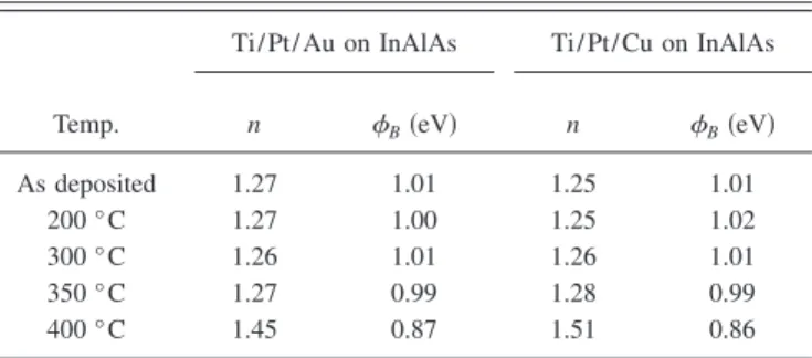
The barrier heights 共B兲 and the ideality factors 共n兲 of
the Ti/ Pt/ Cu and the Ti/ Pt/ Au Schottky contact on InAlAs under various annealing temperatures are summarized in Table I. For the as-deposited Ti/ Pt/ Cu contact, the barrier
a兲Author to whom correspondence should be addressed; electronic mail:
TABLE I. Barrier heights 共B兲 and ideality factors 共n兲 of the Schottky
contact under various annealing temperatures.
Temp.
Ti/ Pt/ Au on InAlAs Ti/ Pt/ Cu on InAlAs
n B共eV兲 n B共eV兲 As deposited 1.27 1.01 1.25 1.01 200 ° C 1.27 1.00 1.25 1.02 300 ° C 1.26 1.01 1.26 1.01 350 ° C 1.27 0.99 1.28 0.99 400 ° C 1.45 0.87 1.51 0.86
APPLIED PHYSICS LETTERS 89, 083517共2006兲
0003-6951/2006/89共8兲/083517/3/$23.00 89, 083517-1 © 2006 American Institute of Physics
This article is copyrighted as indicated in the article. Reuse of AIP content is subject to the terms at: http://scitation.aip.org/termsconditions. Downloaded to IP: 140.113.38.11 On: Thu, 01 May 2014 01:51:40
height and the ideality factor were 1.01 eV and 1.25, respec-tively, while they were similarly 1.01 eV and 1.27 for Ti/ Pt/ Au. Both Ti/ Pt/ Cu and Ti/ Pt/ Au exhibited an excel-lent thermal stability up to 350 ° C annealing. It means that Ti/ Pt/ Cu on InAlAs is a good Schottky contact and has comparable electrical performance as the conventional Ti/ Pt/ Au on InAlAs. The corresponding I-V characteristics of the Ti/ Pt/ Cu Schottky diodes as a function of the anneal-ing temperature were shown in Fig. 1共a兲. The leakage current density of the as-deposited sample was about 3.8 ⫻10−7A / cm2 at −1 V bias. However, the characteristics of the Ti/ Pt/ Cu contacts became Ohmic-like behavior when the annealing temperature exceeded 400 ° C. Figure 1共b兲 shows the barrier heights of the samples subjected to two different surface pretreatments before the deposition of the Ti/ Pt/ Cu. In Fig. 1共b兲, the pretreatment using N2plasma increased the barrier heights from 1.03 to 1.08 eV after 300 ° C annealing. It might be due to the defects generated on the InAlAs layer by the ion bombardment caused by the N2plasma. The bar-rier height of the sample using HCl pretreatment remained stable共1.01 eV兲 even after 300 °C annealing. As a result, the HCl pretreatment was applied for the Ti/ Pt/ Cu Schottky contact fabrication and material analysis in this study.
Figure 2 shows the AES depth profiles for the Ti/ Pt/ Cu as deposited and after annealing. As can be seen from Fig. 2共b兲, the interface of Ti/Pt/Cu on InAlAs remained sharp after 350 ° C annealing, indicating that the Pt was an effec-tive diffusion barrier after 350 ° C annealing. However, the Cu atoms began to penetrate through Pt layer after 400 ° C annealing, as shown in Fig. 2共c兲. Moreover, some Cu atoms and accumulated Ti atoms were found at the interface be-tween Ti and InAlAs layers in Fig. 2共c兲. A mechanism pro-posed in the recent work14 revealed the Ti interdiffusion and possible formation of TiAsxin the Ti/ InAlAs interface
resulted in the degradation of Ti/ Pt/ Au gate on InAlAs/ InGaAs HEMTs. This is consistent with the degra-dation of the Ti/ Pt/ Cu Schottky characteristics that were found in this study with the barrier height dropped to 0.86 eV and the ideal factor increased to 1.51 after 400 ° C annealing, as shown in Table I. Figure 3 are the
cross-sectional TEM micrographs of the Ti/ Pt/ Cu on InAlAs after 350 and 400 ° C annealings for 30 min, respectively. No sig-nificant interface reaction between the Ti/ InAlAs and Ti/ Pt interfaces was observed in Fig. 3共a兲. The interface of Cu/Pt was no longer distinguishable after 400 ° C annealing in Fig. 3共b兲. A dark area observed at the InAlAs layer close to the Ti/ InAlAs interface is due to the diffusion of Ti and Cu into Ti/ InAlAs interface region as judged from the AES depth profile in Fig. 2共c兲. This resulted in the degradation of the FIG. 1.共a兲 I-V characteristics of the Schottky diodes with various annealing
temperatures;共b兲 barrier height vs annealing temperature for the diodes with two different surface pretreatments.
FIG. 2. Auger depth profiles of the Ti/ Pt/ Cu on InAlAs共a兲 as deposited, 共b兲 after annealing at 350 ° C, and共c兲 after annealing at 400 °C.
083517-2 Lien et al. Appl. Phys. Lett. 89, 083517共2006兲
This article is copyrighted as indicated in the article. Reuse of AIP content is subject to the terms at: http://scitation.aip.org/termsconditions. Downloaded to IP: 140.113.38.11 On: Thu, 01 May 2014 01:51:40
Schottky characteristics. Figure 4 shows the XRD results of the Ti/ Pt/ Cu samples as deposited and after annealing for 30 min. From the XRD data, the Ti/ Pt/ Cu on InAlAs struc-ture was quite stable up to 350 ° C annealing and the peaks of Cu, Pt, and Ti remained unchanged. Additional peaks in the XRD pattern emerged after 400 ° C annealing. The addi-tional two peaks were identified as the orthorhombic Cu4Ti共011兲 and Cu4Ti共102兲 phases 共Ref. 17兲. The new for-mation of the phases was due to the Ti interdiffusion and Ti reaction with Cu that resulted in the decrease of the intensity of the Ti peak. This was further investigated using EDX in the Ti layer of the InAlAs/ Ti/ Pt/ Cu structure after 350 and 400 ° C annealings, as shown in Figs. 5共a兲 and 5共b兲, respec-tively. Cu signal appeared only in Fig. 5共a兲 and not in Fig. 5共b兲. The XRD and EDX data indicate that the Pt is a good diffusion barrier for preventing Cu from diffusing into the Ti/ Pt/ Cu Schottky structure up to 350 ° C. However, atomic interdiffusion occurred after 400 ° C annealing. The forma-tion of Cu4Ti implies that Cu atoms had diffused through the Pt layer and reacted with the Ti layer at 400 ° C. The results show good consistency with the AES depth profile and the TEM data in Figs. 2 and 3.
Excellent electrical characteristics of the Ti/ Pt/ Cu Schottky contact on InAlAs were observed with the ideality factor and the barrier height of 1.25 and 1.01 eV, respec-tively, and the data remained almost the same after 350 ° C annealing. The material analysis showed that no interfacial phase was formed after 350 ° C annealing and that Pt had successfully blocked the Cu diffusion into the underlying layers. After 400 ° C annealing, the Cu began to penetrate
through the diffusion barrier and formed intermetallic com-pound of Cu4Ti. Meanwhile the diffusion of Ti and Cu into Ti/ InAlAs interface region was observed in AES depth pro-file, which was responsible for the rise of the ideal factor and the lowering of the effective barrier height. The results show that Ti/ Pt/ Cu Schottky contact to InAlAs is very stable up to 350 ° C annealing and that Cu metallization using Pt as the diffusion barrier can be integrated into the front-side metal-lization for the InAlAs/ InGaAs HEMTs and MMICs.
The authors would like to acknowledge the support from the National Science Council, and the Ministry of Economic Affairs, Taiwan, R.O.C., under Contracts Nos. NSC 95-2752-E-009-001-PAE and 94-EC-17-A-05-S1-020.
1K. Holloway, P. M. Fryer, C. Cabral, Jr., J. M. E. Harper, P. J. Bailey, and
K. H. Kelleher, J. Appl. Phys. 71, 5433共1992兲.
2D. S. Yoon, H. K. Baik, and S. M. Lee, J. Appl. Phys. 83, 8074共1998兲. 3M. T. Wang, Y. C. Lin, and M. C. Chen, J. Electrochem. Soc. 145, 2538
共1998兲.
4L. Arnaud, G. Tartavel, T. Berger, D. Mariolle, Y. Gobil, and I. Touet,
Microelectron. Reliab. 40, 77共2000兲.
5S. Q. Hong, C. M. Comrie, S. W. Russell, and J. W. Mayer, J. Appl. Phys. 70, 3655共1991兲.
6M. Offenberg, M. Liehr, G. W. Rubloff, and K. Holloway, Appl. Phys.
Lett. 47, 1254共1990兲.
7P. H. Wohlbier, Diffusion and Defect Data 10, 89共1975兲.
8C. Y. Chen, E. Y. Chang, L. Chang, and S. H. Chen, IEEE Trans. Electron
Devices 48, 1033共2001兲.
9H. C. Chang, E. Y. Chang, Y. C. Lien, L. H. Chu, S. W. Chang, R. C.
Huang, and H. M. Lee, Electron. Lett. 39, 1763共2003兲.
10M. O. Aboefotoh, C. L. Lin, and J. M. Woodall, Appl. Phys. Lett. 65,
3245共1994兲.
11K. Shinohara, Y. Yamashita, A. Endoh, I. Eatanabe, K. Hikosaka, T.
Matsui, T. Mimura, and S. Hiyamizu, IEEE Electron Device Lett. 25, 241 共2004兲.
12S. W. Chang, E. Y. Chang, C. S. Lee, K. S. Chen, C. W. Tseng, Y. Y. Tu,
and C. T. Lee, Jpn. J. Appl. Phys., Part 2 44, L899共2005兲.
13J.-P. Ao, D. Kikuta, N. Kubota, Y. Naoi, and Yasuo Ohno, IEEE Electron
Device Lett. 24, 500共2003兲.
14Y. C. Chou, D. Leung, R. Grundbacher, R. Lai, P. H. Liu, Q. Kan, M.
Biedenbender, D. Eng, and A. Oki, IEEE Electron Device Lett. 25, 351 共2004兲.
15Y. C. Chou, R. Grundbacher, D. Leung, R. Lai, Q. Kan, D. Eng, P. H. Liu,
T. Block, and A. Oki, in Proceedings of Indium Phosphide and Related Materials, 2005, p. 223.
16G. Stareev, H. Kunzel, and G. Dortmann, J. Appl. Phys. 74, 7344共1993兲. 17JCPDS PDF No. 20-0370共unpublished兲.
FIG. 3. Cross-sectional TEM micrographs of the Ti/ Pt/ Cu on InAlAs共a兲 after 350 ° C annealing and共b兲 after 400 °C annealing.
FIG. 4. XRD results of Ti/ Pt/ Cu on InAlAs with various annealing temperatures.
FIG. 5. EDX of the Ti layer of the InAlAsTi/ Pt/ Cu structure after annealing at共c兲 350 °C and 共d兲 400 °C.
083517-3 Lien et al. Appl. Phys. Lett. 89, 083517共2006兲
This article is copyrighted as indicated in the article. Reuse of AIP content is subject to the terms at: http://scitation.aip.org/termsconditions. Downloaded to IP: 140.113.38.11 On: Thu, 01 May 2014 01:51:40