IEEE PHOTONICS TECHNOLOGY LETTERS, VOL. 21, NO. 15, AUGUST 1, 2009 1039
A
W -Band Photonic Transmitter-Mixer Based on
High-Power Near-Ballistic Uni-Traveling-Carrier
Photodiodes for BPSK and QPSK Data Transmission
Under Bias Modulation
Jin-Wei Shi, F.-M. Kuo, Y.-S. Wu, Nan-Wei Chen, Po-Tsung Shih, Chun-Ting Lin, Wen-Jr Jiang, Er-Zih Wong,
Jason (Jyehong) Chen, and Sien Chi
Abstract—In this study, we demonstrate wireless binary phase-shift keying (BPSK) and quadrature phase-shift keying (QPSK) data transmission at the -band by use of bias modu-lation on photonic transmitters-mixers, which are composed of near-ballistic uni-traveling-carrier photodiodes and quasi-Yagi antennas without the integration of an Si-lens. By use of such a device and a novel optical millimeter-wave source with octupling optical frequency, we can successfully achieve 1.25-Gb/s BPSK and 0.625-Gb/s QPSK data-transmission at 105 GHz with 5-GHz intermediate-frequency signals.
Index Terms—High-power photodiode, optoelectronic mixer, photodiode, photonic transmitter.
I. INTRODUCTION
T
HE tremendous increase in the required volume of wireless data-transmission has stimulated attention on ways to use the millimeter-wave (MMW) bands above 60 GHz ( -band) or above 100 GHz ( -band) as the carrier frequency for the realization of systems with very high transmission data rates in excess of many gigabits-per-second [1], [2]. Unfortunately, there is a large propagation loss of the MMW signal in the -band or -band frequencies, whether in free space or in a coaxial cable. One promising solution to this problem is the radio-over-fiber (ROF) technique [1], [2], where the MMW signal is distributed through a lossless optical fiber and then radiated over the last-mile to the user-end. Recently, a research group at NTT reported excellent results for a 10-Gb/s wireless link at 120 GHz, achieved by using a uni-traveling-carrier photodiode (UTC-PD)-based photonic transmitter [1], [2]. In order to eliminate the serious fading and time-shifting effects induced by fiber chromatic dispersion of the data signal with the high-frequency local-oscillator (LO) signal at the - or -bands, two different optical wave-lengths are usually adopted for the data and LO signals [3], [4]Manuscript received February 12, 2009; revised March 31, 2009. First pub-lished May 08, 2009; current version pubpub-lished July 10, 2009.
J.-W. Shi, F.-M. Kuo, Y.-S. Wu, and N.-W. Chen are with the Department of Electrical Engineering of National Central University, Taoyuan 320, Taiwan (e-mail: [email protected]).
P.-T. Shih, C.-T. Lin, W.-J. Jiang, E.-Z. Wong, and J. Chen are with the De-partment of Photonics, National Chiao-Tung University, Hsinchu 300, Taiwan (e-mail: [email protected]; [email protected]).
S. Chi is with the Department of Electrical Engineering, Yuan Ze University, TaoYuan 320, Taiwan.
Color versions of one or more of the figures in this letter are available online at http://ieeexplore.ieee.org.
Digital Object Identifier 10.1109/LPT.2009.2021274
in the ROF system. An additional high-frequency MMW mixer or electrooptic (E-O) modulator is usually necessary at the base station to up-convert the data signal to the LO frequency and then radiate the up-converted signal to the user-end [3]. The idea of utilizing the nonlinearity of high-speed PDs [4], [5], such as UTC-PDs, to realize this up-conversion process is very attractive, because this could eliminate the necessity of the high-frequency electronic mixer or E-O modulator [5]. To use such a technique, it is necessary to swing the bias of UTC-PD to the forward bias regime in order to get a high extinction ratio of modulated MMW power. However, this approach limits its modulation bandwidth performance [5]. Furthermore, it is usually necessary to integrate an additional Si-lens with such a photonic transmitter to overcome the substrate-mode problem [2] of the antenna. The monolithic integration of uniplanar high-directivity Yagi–Uda antenna with UTC-PD to serve as the photonic emitter is another possible good solution, which eliminates the necessity of additional Si-lens [6]. In our previous work [7], [8], we demonstrated a photonic trans-mitter/mixer that operated at the -band. The device consisted of a high-speed high-power near-ballistic uni-traveling-carrier photodiode (NBUTC-PD) [9] and a planar quasi-Yagi antenna [7], [8] on an aluminum–nitride (AlN) substrate. The device was insensitive to the aforementioned substrate modes and thus did not call for the integration of an additional Si-lens. By utilizing the strong bias-dependent nonlinearity of speed of NBUTC-PD under a reverse bias regime, our transmitter could also serve as a photonic mixer, generating high-power up-con-verted MMW signals with a wide modulation bandwidth [10]. In this current work, we demonstrate wireless data transmission at the -band (105 GHz) using a novel optical MMW source with octupling optical frequency [11] and our device under a bias modulation of 1.25-Gb/s binary phase-shift keying (BPSK) and 0.625-Gb/s quadrature phase-shift keying (QPSK) data modulation format with a 5-GHz intermediate-frequency (IF) signal. As compared to the demonstrated on–off keying (OOK) data format and linear photodetection scheme in previous work [1], [2], the demonstrated QPSK with bias modulation on NBUTC-PD for wireless data transmission can have a higher spectral efficiency and more suitable for the application to the long-reach ( 100 km) optical-wireless access network [3], [4].
II. DEVICESTRUCTURE ANDMEASUREMENTSETUP
Fig. 1 shows a top view of the demonstrated device. The de-vice consists of a diced NBUTC-PD chip with a 100 m active
1040 IEEE PHOTONICS TECHNOLOGY LETTERS, VOL. 21, NO. 15, AUGUST 1, 2009
Fig. 1. Top-view of the demonstrated device;.
Fig. 2. (a) Measured (closed squares) and simulated (open squares) radiation patterns for the demonstrated device at theE-plane. (b) Simulated S param-eter (close squares) and the detected power (open circles) spectrum.
area, which exhibits a 100-GHz optical-to-electrical bandwidth under a 25- load resistance with a responsivity of 0.15 A/W [9] and a quasi-Yagi planar antenna chip. The whole module is formed on an AlN substrate, giving it good thermal con-ductivity for high-power operation. The antenna chip is com-prised of a quasi-Yagi antenna [7], [8]. The fan-shaped broad-band transition between the coplanar waveguide and the slot-line acts as an impedance matching circuit. A flip-chip bonded active NBUTC-PD, an IF signal input port, a -band radio-fre-quency (RF) choke, and bond pads for the dc bias are also in-cluded. Compared to our previous work [7], we have increased the number of directors and modified the geometric size of the antenna, which increases its directivity and bandwidth. The sim-ulated gain and directivity of the quasi-Yagi antenna at around the center operating frequency (100 GHz) is 9.4 and 9.8 dB, re-spectively. During measurement, the optical LO signal is gen-erated by the heterodyne-beating technique. The modulated op-tical signal is then focused on the microlens [9] on the back-side of the diced NBUTC-PD by a lensed fiber. The LO signal with the up-converted RF signals are all radiated to free-space through the quasi-Yagi antenna to be detected by a standard horn antenna at the -band (with a 24 dB gain), which is connected to a -band mixer (Agilent 11970W) and a spectrum analyzer (Agilent E444BA).
III. MEASUREMENTRESULTS
The simulated and measured radiation patterns at the -plane of the photonic transmitter are shown in Fig. 2(a). As can be seen, they are in excellent agreement. Fig. 2(b) shows the sim-ulated of the quasi-Yagi antenna without considering the integrated active device and the measured frequency response of the detected power of our transmitter as the LO frequency sweeps from 75 to 110 GHz. We can clearly see that a significant resonance of radiated power exists at around 100 GHz, which is consistent with the of the quasi-Yagi antenna. Fig. 3(a) shows the detected up-converted RF power versus the injected electrical IF power under a fixed optical LO power (21 dBm) and an optimum bias point ( 1.5 V) for mixer operation. The 1-dB compression points of the up-converted RF power ( 32 dBm)
Fig. 3. (a) Up-converted RF power versus IF power under01.5 V and 21 dBm optical LO power injection. (b) Maximum detected power versus photocurrent for an operating frequency fixed at 100 GHz under bias voltages of03 and 05 V.
Fig. 4. System setup for BPSK or QPSK data transmission.
and injected IF power (7.5 dBm) are both specified in Fig. 3. In addition to the up-converted RF power, the maximum radi-ated LO power under high reverse bias (over 2.5 V) is also an important factor for evaluating the performance of a photonic transmitter. Fig. 3(b) shows the detected MMW power of the device. We achieve a 100- m active area under optical signal injection with a 100% modulation depth, as a function of the photocurrent under bias voltages of 3 and 5 V. As indicated on the plot, the maximum detected power is 14 dBm, obtained when the photocurrent is around 30 mA. Fig. 4 shows the system setup for BPSK or QPSK data transmission. Compared to the traditional OOK data transmission process [1] using a photonic transmitter, the modulation format of the BPSK and QPSK tech-niques allows for higher spectral efficiency and is compatible with today’s wireless communication systems. In order to re-alize the goal of free-space data transmission, we also develop a high-performance -band optical photonic source [11]. The inset to Fig. 4 shows the output optical spectrum from this op-tical source. As can be seen, the opop-tical harmonic distortion sup-pression ratio is 18 dB, and is limited by the bandwidth of our dual-parallel E-O modulator (i.e., 10 GHz) [11]. This source is much less noisy than the two-laser heterodyne-beating system, which was used for device characterization. During the exper-iment, the BPSK signal is a 1.25-Gb/s pseudorandom bit se-quence signal. The 0.625-Gb/s QPSK signal is gener-ated by an arbitrary waveform generator (AWG) at a data rate of 625 Mb/s. Both kinds of signal are up-converted with an analog IF signal at 5 GHz by the use of an electronic mixer. The mixed signal is then fed into the IF input port of the photonic emitter/ mixer to modulate the bias point of the device. The injected IF power is around 2 dBm, which corresponds to around V (peak-to-peak) amplitude of driving voltage. The modulation
SHI et al.: -BAND PHOTONIC TRANSMITTER-MIXER BASED ON HIGH-POWER NBUTC-PDs FOR BPSK AND QPSK 1041
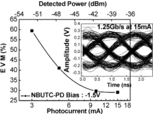
Fig. 5. Measured EVM versus received MMW power and output photocurrent. The inset shows the reconstructed BPSK eye-pattern at 1.25 Gb/s.
Fig. 6. (a) Constellation of the 0.625-Gb/s QPSK signal. Eye diagrams of the 0.625-Gb/s QPSK signal: (b)I; (c) Q.
frequency of the optical LO signal from the photonic source is 100 GHz. The 1.25-Gb/s BPSK or 0.625-Gb/s QPSK signal is thus up-converted to 105 GHz (LO: 100 GHz. IF: 5 GHz) and then radiated to the receiving end. The receiver end is com-posed of a -band horn antenna, a -band low-noise-amplifier (QuinStar: QLW-90a06030-P1), and a fast -band power de-tector (Militech: DXP-10-RPFW0) to detect the envelope and phase of data signal at 5-GHz IF. The signal detected by the power detector is boosted by an IF amplifier and then fed into a high-speed real-time scope prior to performing off-line signal processing [8], [11]. The transmission distance is around 5 cm, which can further be increased by increasing the directivity of used antenna [1]. Fig. 5 shows the output photocurrent of trans-mitter or received MMW power versus the error vector mag-nitude (EVM) of the transmitted data. The EVM is defined as
, where and are the received and ideal symbols, respectively, and
is the maximum symbol vector in the constellation. The inset shows the reconstructed BPSK pattern with clear eye-opening at 1.25 Gb/s under a photocurrent of 15 mA. As can be seen, when the MMW power received MMW reaches 42 dBm
and the output photocurrent reaches 10 mA, the measured EVM can be less than around 30%.
Fig. 6(a) shows the constellation of the received 0.625-Gb/s QPSK signal when the output photocurrent is 10 mA; while (b) and (c) show the digital signal processing reconstructed and eye diagrams. The corresponding EVM is around 24.7%. According to the measured frequency response of our system (channel), we can expect a higher data transmission rate ( 1.25 Gb/s) by increasing the bandwidth of the -band power detector and the IF frequency ( 5 GHz).
IV. CONCLUSION
In this study, we devise an NBUTC-PD based -band photonic transmitter/mixer. This novel device can be used with an optical MMW source, to realize 1.25-Gb/s BPSK and 0.625-Gb/s QPSK wireless data transmission at 105 GHz under direct bias modulation.
REFERENCES
[1] A. Hirata, T. Kosugi, H. Takahashi, R. Yamaguchi, F. Nakajima, T. Fu-ruta, H. Ito, H. Sugahara, Y. Sato, and T. Nagatsuma, “120-GHz-band millimeter-wave photonic wireless link for 10-Gb/s data transmission,”
IEEE Trans. Microw. Theory Tech., vol. 54, no. 5, pp. 1937–1944, May
2006.
[2] A. Hirata, H. Ishii, and T. Nagatsuma, “Design and characteriza-tion of a 120-GHz millimeter-wave antenna for integrated photonic transmitters,” IEEE Trans. Microw. Theory Tech., vol. 49, no. 11, pp. 2157–2162, Nov. 2001.
[3] H.-C. Chien, A. Chowdhury, Z. Jai, Y.-T. Hsueh, and G.-K. Chang, “Long-reach 60-GHz Mm-wave optical-wireless access network using remote signal regeneration and upconversion,” in Proc. ECOC 2008, Brussels, Belgium, Germany, Sep. 2008, vol. 2, pp. 137–138. [4] M. Tsuchiya and T. Hosida, “Nonlinear photodetection scheme and
its system applications to fiber-optic millimeter-wave wireless down-links,” IEEE Trans. Microw. Theory Tech., vol. 47, no. 7, pt. 2, pp. 1342–1350, Jul. 1999.
[5] A. Hirata, T. Furuta, H. Ito, and T. Nagatsuma, “10-Gb/s millimeter-wave signal generation using photodiode bias modulation,” J. Lightw.
Technol., vol. 24, no. 4, pp. 1725–1731, Apr. 2006.
[6] A. Hirata, T. Furuta, and T. Nagatsuma, “Monolithically integrated Yagi-Uda antenna for photonic emitter operating at 120 GHz,”
Elec-tron. Lett., vol. 37, no. 18, pp. 1107–1109, Aug. 2001.
[7] Y. S. Wu, N. W. Chen, and J. W. Shi, “AW -band photonic trans-mitter/mixer based on high-power near-ballistic uni-traveling-carrier photodiode (NBUTC-PD),” IEEE Photon. Technol. Lett., vol. 20, no. 21, pp. 1799–1801, Nov. 1, 2008.
[8] Y. S. Wu, F. M. Kuo, S. N. Wang, N. W. Chen, J. W. Shi, P. T. Shih, C. T. Lin, W. J. Jiang, E. Z. Wong, J. Chen, and S. Chi, “A W-Band pho-tonic transmitter-mixer based on high-power near-ballistic uni-trav-eling-carrier photodiode (NBUTC-PD) for 1.25-Gb/s BPSK data trans-mission under bias modulation,” in Proc. OFC 2009, San Diego, CA, Mar. 2009, Paper OWX3.
[9] Y.-S. Wu and J.-W. Shi, “Dynamic analysis of power and high-speed near-ballistic unitraveling carrier photodiodes atW -band,” IEEE
Photon. Technol. Lett., vol. 20, no. 13, pp. 1160–1162, Jul. 1, 2008.
[10] J.-W. Shi, Y.-S. Wu, and Y.-S. Lin, “Near-ballistic uni-traveling-carrier photodiode basedV -band optoelectronic mixers with internal up-con-version-gain, wide modulation bandwidth, and very high operation cur-rent performance,” IEEE Photon. Technol. Lett., vol. 20, no. 11, pp. 939–941, Jun. 1, 2008.
[11] P. T. Shih, C. T. Lin, W. J. Jiang, E. Z. Wong, J. Chen, S. Chi, Y.-S. Wu, F.-M. Kuo, N.-W. Chen, and J.-W. Shi, “W -band vector signal generation via optical millimeter-wave generation and direct modula-tion of NBUTC-PD,” in Proc. OFC 2009, San Diego, CA, Mar. 2009, Paper OWP4.