國 立 交 通 大 學
電子工程學系電子研究所
碩
碩
碩
碩 士
士
士
士 論
論
論
論 文
文
文
文
釩摻雜與快速熱退火應用於以濺鍍法製備之鋯酸鍶
記憶體元件電阻轉換特性研究
E
EE
Effects
ffects
ffects of Vanadium Doping and Rapid Thermal
ffects
of Vanadium Doping and Rapid Thermal
of Vanadium Doping and Rapid Thermal
of Vanadium Doping and Rapid Thermal
Annealing
Annealing
Annealing
Annealing
o
oo
on Sputter
n Sputter
n Sputter
n Sputter-
--
-D
Deposited SrZrO
DD
eposited SrZrO
eposited SrZrO
eposited SrZrO
3333Resistive
Resistive
Resistive
Resistive
Switching
Switching
Switching
Switching Memory Device
Memory Device
Memory Device
Memory Device
研 究 生:詹世偉
指導教授:曾俊元
釩摻雜與快速熱退火應用於以濺鍍法製備之鋯酸鍶記憶體元件電
阻轉換特性研究
Effects
Effects
Effects
Effects of V
of V
of Vanadium D
of V
anadium D
anadium D
anadium Doping and R
oping and R
oping and Rapid
oping and R
apid
apid T
apid
TT
Thermal
hermal A
hermal
hermal
AA
Annealing
nnealing
nnealing
nnealing
o
oo
on
n
n
n
Sputter
Sputter
Sputter
Sputter-
--
-D
DD
Deposited SrZrO
eposited SrZrO
eposited SrZrO
eposited SrZrO
3333Resistive Switching
Resistive Switching Memory Device
Resistive Switching
Resistive Switching
Memory Device
Memory Device
Memory Device
研 究 生:詹世偉
Student: Shih-Wei Jan
指導教授:曾俊元
Advisor: Tseung-Yuen Tseng
國立交通大學 電子工程學系電子研究所
碩 士 論 文
A Thesis
Submitted to Department of Electronics Engineering and Institute of Electronics
College of Electrical and Computer Engineering National Chiao Tung University
in partial Fulfillment of the Requirements for the Degree of
Master
in Electronics Engineering July 2008
Hsinchu, Taiwan, Republic of China
釩摻雜與快速熱退火應用於以濺鍍法製備之鋯酸鍶記憶體元件電
阻轉換特性研究
研究生:詹世偉 指導教授:曾俊元
國立交通大學
電子工程學系電子研究所
摘要
摘要
摘要
摘要
本論文利用鈣鈦礦結構材料(鋯酸鍶)作為電阻式記憶體的材料,首先將介紹新世 代非揮發性記憶體之應用、特性以及優點,也將探討各種可能的電阻轉換機制及傳導機 制。在實驗的部分,我們利用射頻磁控濺鍍法製備純鋯酸鍶與釩摻雜鋯酸鍶薄膜作為轉 換電阻層,且利用此濺鍍法沉積鎳酸鑭作為幫助鋯酸鍶成長優選方向之緩衝層,底電極 白金及頂電極鋁則利用蒸鍍法製備,形成一頂電極/電阻層/緩衝層/底電極的結構。首 先,將探討釩摻雜對鋯酸鍶薄膜轉態特性之影響,我們製作不同濃度釩摻雜的鋯酸鍶記 憶體元件,發現釩摻雜有助於穩定電阻轉換特性,更進一步由實驗結果及佐證來探討可 能的電阻轉換機制。第二部份將鋯酸鍶薄膜利用快速熱退火改善其電阻轉換特性並趨於 穩定,其中以氧氣在攝氏 600 度進行熱退火可使元件具有穩定的電阻轉換特性,同時也 比較及探討不同快速熱退火條件對記憶體元件特性的影響,包含不同熱退火溫度、不同 熱退火時間及不同熱退火氣體,由實驗結果推測以氧氣進行快速熱退火可修補鋯酸鍶薄 膜中的缺陷,進而穩定電阻轉換特性。Effects of Vanadium D
Effects of Vanadium D
Effects of Vanadium D
Effects of Vanadium Doping and Rapid Thermal Annealing on
oping and Rapid Thermal Annealing on
oping and Rapid Thermal Annealing on
oping and Rapid Thermal Annealing on
Sputter
Sputter
Sputter
Sputter-
--
-D
DD
Deposited SrZrO
eposited SrZrO
eposited SrZrO
eposited SrZrO
3333Resistive Switching
Resistive Switching
Resistive Switching
Resistive Switching Memory Device
Memory Device
Memory Device
Memory Device
Student: Shih-Wei Jan
Advisor: Tseung-Yuen Tseng
Department of Electronics Engineering and Institute of Electronics
National Chiao Tung University
Abstract
In this thesis, the RRAM devices manufactured based on SrZrO3 (SZO) thin films are
studied and developed. At first, I will introduce the applications, fundamental characteristics, and advantages of next-generation nonvolatile memories. The conduction mechanisms of RRAM that have been published are also discussed. In experimental details, pure-SZO and V doped SZO film was deposited on the LaNiO3 buffer layer by RF magnetron sputter. Pt and
Al act as bottom electrode and top electrode, respectively. Therefore, electrode/resistive thin film/buffer layer/electrode structure is formed. First, we will discuss the influence of V-doping effect. We fabricate different V-dopant concentration SZO memory devices. The switching property can be stabilized by V-doping. We confer the resistive switching mechanism by experiment results and proofs. Second, we use thermal treatment to improve and stabilize the switching property by rapid thermal annealing (RTA) on SZO film. The SZO memory device has the stable switching property by RTA at 600℃ with O2. The effects of
resistive switching property by different RTA conditions are also compared and discussed. The RTA conditions include different RTA temperature, different RTA time and different RTA gas. We conjecture that the defects of SZO film can be repaired by RTA with O2. Then,
誌謝
感謝指導教授曾俊元老師,提供豐富的研究資源及研究環境,讓我順利
進行實驗及學術研究,並在專業領域上給予許多的指導,使得我能有機會
不斷的學習與成長,還有感謝老師在生活上給予關懷。能跟隨老師學習,
是我最大的光榮。
感謝林孟漢學長、林群傑學長、林志洋學長、姚奕全學長,在我實驗、
課業以及論文上給予我很多的指教,並能隨時指出我的錯誤,讓我能夠在
這兩年安然地度過。還要感謝吳明錡學長、王勝裕學長、李岱螢學長,在
實驗上也給予我很大的協助。還有黃毅函、顏宏全、翁啟翔、這幾位同學,
同時也是很好的朋友,感謝你們課業及研究上的互相幫忙,生活上遇到困
難你們也會即時給予協助,有喜怒哀樂也能和你們一同分享,我會珍惜這
段難忘的回憶及友誼。還有葉昱廷、李盈賢、孫淑炫、蔡承翰、黃志文這
幾位學弟學妹,多謝你們在實驗上的幫忙。還有感謝許多幫助過我的朋友。
感謝我的家人,感謝你們支持我念完研究所,有你們的支持我才能順利
完成研究所學業取得碩士學位。還要感謝我的女友,在我壓力大和心情低
落時能體諒我、鼓勵我,給我許多關懷,真的很感謝。
Contents
Chinese Abstract ………. i
English Abstract ……….. ii
Acknowledgement……….………….. iii
Contents ………... iv
Table Captions ………. vii
Figure Captions ………... viii
Chapter 1 Introduction 1 1.1 Introduction to Memories ………. 1
1.1.1 Volatile Memory ……….... 1
1.1.2 Nonvolatile Memory ………. 5
1.2 Resistive Random Access Memory………...…… 14
1.2.1 The Structure and Operation Method of RRAM……… 15
1.2.2 Material Groups of RRAM……… 16
1.3 Resistive Switching Properties of Doped SrZrO3 Films………... 16
Chapter 2 Experiment Details 24 2.1 Experiment Process Flow ………. 24
2.2 RF Magnetron Sputter Systems………. 25
2.2.1 Vacuum System ………. 25
2.2.2 Pressure System ………. 25
2.2.3 Temperature Controlling System ………... 26
2.2.4 Gas Flow Controlling System ………... 26
2.2.5 Plasma Controlling System ………... 26
2.3 Preparation of Devices ………. 27
2.3.1 Preparation of Sputter Targets ………... 27
2.3.2 Thin Film Depositions ………... 29
2.3.3 Heat Treatment after Thin Film Depositions ………. 29
2.3.4 Deposition of Top Electrode ……….. 30
2.4 Measurements and Analyses ……… 30
2.4.1 X-Ray Diffraction ………. 30
2.4.2 Scanning Electron Microscope ……….. 31
2.4.3 Focus Ion Beam ……….… 31
2.4.4 Field Emission Transmission Electron Microscope and Energy Dispersive X-Ray Spectrometer ………. 32
2.4.5 Auger Electronic Microscopy ……….. 33
2.4.6 Secondly Ion Mass Spectrometer………... 33
2.4.7 Current-Voltage Measurements ………. 34
Chapter 3 Results and Discussion 39 3.1 Experiments Contents………..………. 39
3.2 Properties and Analyses of the LaNiO3 Buffer Layer and SrZrO3 Resistive Films 39 3.2.1 X-Ray Diffraction and Scanning Electronic Microscope of LaNiO3 Buffer Layer and SrZrO3 Thin Film………..……… 39
3.2.2 Transmission Electron Microscope ………... 40
3.3 Electrical and Physical Properties of the Pure and V-doped SrZrO3 memory films 41 3.3.1 Nonpolar Switching Property of SrZrO3 Resisitve Film………. 41
3.3.2 Forming Process of the Pure and V-doped SrZrO3………. 42
3.3.3 Electrical Properties of the Pure and V-doped SrZrO3………... 42
3.3.5 Retention………..………... 44
3.3.6 Non-Destructive Readout……… ………... 44
3.3.7 Conduction Mechanisms of Pure and V-doped SrZrO3……….. 45
3.3.8 Barrier Height………... 45
3.3.9 High-Temperature Measurement……… 46
3.3.10 Resistive Switching Mechanism……….. 47
3.3.11 Summaries of Vanadium Doping Influence………. 48
3.4 Effects of Rapid Thermal Annealing on Pure-SrZrO3 Thin Film……….. 48
3.4.1 X-Ray Diffraction of the SrZrO3 Thin Film by Rapid Thermal Annealing…. 49 3.4.2 Scanning Electron Microscope Analyses of the SrZrO3 Thin Film…………. 49
3.4.3 Transmission Electron Microscope………. 49
3.4.4 Auger Electron Microscope………. 50
3.4.5 Secondary Ion Mass Spectrometer……….. 50
3.4.6 Endurance………... 50
3.4.7 The Switching Property in Different Operation Mode……… 51
3.4.8 Different RTA Time………. 53
3.4.9 Different Gas RTA……….……….. 54
3.4.10 Retention……….………. 55
3.4.11 Non-Destructive Readout………... 55
3.4.12 Conduction Mechanism……… 56
3.4.13 Forming Process……….... 56
3.4.14 Possible Mechanism of Thermal Treatment………. 57
Chapter 4 Conclusion 96
Table Captions
Chapter 3
Table 3-1 The comparison of switching property for W/O RTA, RTA 600℃,
RTA 700 ℃ and RTA 800℃... 58 Table 3-2 The definition of operation mode………... 58 Table 3-3 The comparison of switching property of pure-SZO with different gas
Figure Captions
Chapter 1
Fig. 1-1 Principle of operation of DRAM read (left) and write (right), for
simple 4 by 4 array [5]………... 19 Fig. 1-2 A six-transistor CMOS SRAM cell [6]……….. 19 Fig. 1-3 Typical floating gate memory structure………. 20 Fig. 1-4 Schematic plot of a PCRAM cell. Depending on the state of the active
region (crystalline or amorphous) the resistance of the cell changes by
several orders of magnitude……….. 20 Fig. 1-5 I-V curve of a PCRAM cell. SET and RESET denote the switching
regions, while READ denotes the region of readout……….
21 Fig. 1-6 ABO3 perovskite unit cell [4]……… 21
Fig. 1-7 Hysteresis loop of the ferroelectric material [4]……… 22 Fig. 1-8 Cross section schematic diagram of the RRAM. The transistor is
fabricated in the front and the resistor in the back end [16]…………... 22 Fig. 1-9 Equivalent circuit of an array for the write operation of a given bit
resistor [17]……… 23 Fig. 1-10 Describing how leakage current paths make cell resistance misread
[24]………. 23
Chapter 2
Fig. 2-1 Illustration of the experimental flow………. 36 Fig. 2-2 Preparation flow of the device………... 36 Fig. 2-3 Cross section of the four-layer structure device……… 37
Fig. 2-4 Illustration of the sputter system……… 37
Fig. 2-5 Synthesis flow chart of LNO powder………. 38
Fig. 2-6 Synthesis flow chart of doped SZO powder……….. 38
Chapter 3 Fig. 3-1 XRD of LNO buffer layer and SZO thin film……… 60
Fig. 3-2 SEM surface morphology of the LNO after 600oC RTA treatment…... 60
Fig. 3-3 SEM surface morphology of the LNO after 700oC RTA treatment…... 61
Fig. 3-4 TEM cross section image of the pure-SZO thin film………. 61
Fig. 3-5 The nonpolar switching property of SrZrO3 Resistive Film…………. 62
Fig. 3-6 The forming process by negative bias voltage for each SZO film…… 62
Fig. 3-7 The statistics of forming voltages for each SZO film……… 63
Fig. 3-8 The resistive switching I-V curves of each SZO film……… 63
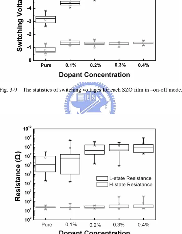
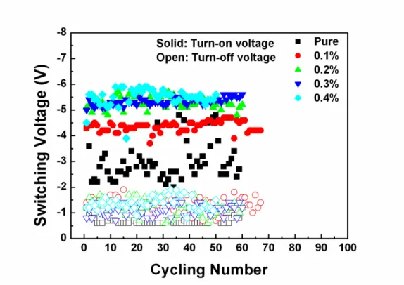
Fig. 3-9 The statistics of switching voltages for each SZO film in –on-off mode……… 64
Fig. 3-10 The resistance statistics of H-state and L-state for each SZO film…… 64
Fig. 3-11 Variation of switching voltage of each SZO memory film device……. 65
Fig. 3-12 Variation of two current state of each SZO memory film device…….. 65
Fig. 3-13 Retention of the pure-SZO memory film device at RT and 85℃…….. 66
Fig. 3-14 Voltage stress of pure-SZO memory film device measured at RT and 85oC……… 66
Fig. 3-15 Current fitting curves of pure-SZO……… 67
Fig. 3-16 Current fitting curves of 0.1% V-doped SZO……… 67
Fig. 3-17 Current fitting curves of 0.2% V-doped SZO………. 68
Fig. 3-19 Current fitting curves of 0.4% V-doped SZO……… 69 Fig. 3-20 Barrier height of each SZO film……… 69 Fig. 3-21 The L-state I-V curves in double nature logarithmic plots at low field
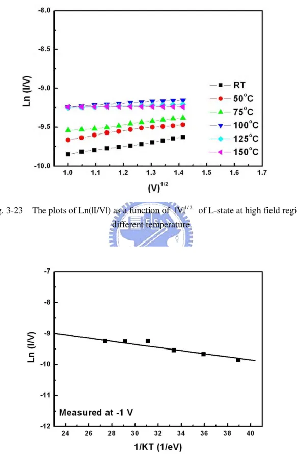
region at different temperature……….. 70 Fig. 3-22 The activation energy of L-state measured at -0.3V………. 70 Fig. 3-23 The plots of Ln(|I/V|) as a function of |V| of L-state at high field 1/ 2
region at different temperature………... 71 Fig. 3-24 The plots of Ln(|I/V|) as a function of 1/KT (1/eV) of L-state
measured at -1V……… 71 Fig. 3-25 The L-state I-V curves in double nature logarithmic plots at low field
region at different temperature………. 72 Fig. 3-26 The activation energy of H-state measured at -0.3V……… 72 Fig. 3-27 Hypothetical diagram of resistive switching mechanism: (a) Original
state, (b)L-state at low field, (c) L-state at high field, and (d) H-state. 73 Fig. 3-28 XRD patterns of SZO films with different O2 RTA temperature…….. 73
Fig. 3-29 SEM surface micro-morphology of the as-deposited pure-SZO film… 74 Fig. 3-30 SEM surface micro-morphology of the pure-SZO after O2 600oC RTA
treatment……….. 74
Fig. 3-31 SEM surface micro-morphology of the pure-SZO after O2 700oC RTA
treatment……… 75
Fig. 3-32 SEM surface micro-morphology of the pure-SZO after O2 800℃
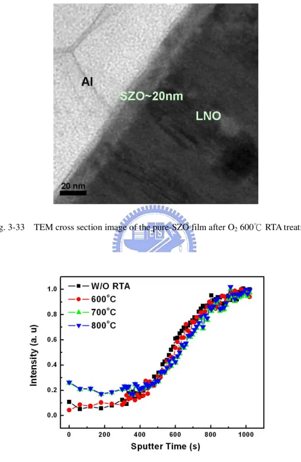
RTA treatment………. 75 Fig. 3-33 TEM cross section image of the pure-SZO film after O2 600℃ RTA
Fig. 3-34 AEM of Lanthanum intensity for pure-SZO and LNO film with
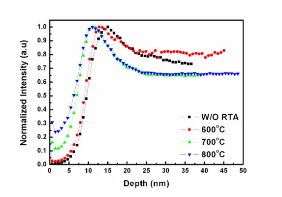
different O2 RTA temperature……… 76
Fig. 3-35 SIMS of Lanthanum intensity for the pure-SZO film with different O2
RTA temperature……… 77 Fig. 3-36 Variation of switching voltage of pure-SZO with O2 RTA 600℃ for
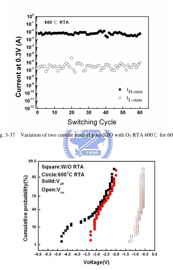
60 sec……… 77
Fig. 3-37 Variation of two current state of pure-SZO with O2 RTA 600℃ for 60
sec………. 78
Fig. 3-38 Cumulative probability of pure-SZO without RTA and with O2 RTA 600
℃ for 60 sec………. 78 Fig. 3-39 Variation of switching voltage of pure-SZO with O2 RTA 700℃ for
60 sec………. 79
Fig. 3-40 Variation of two current state of pure-SZO with O2 RTA 700℃ for 60
sec………. 79
Fig. 3-41 Variation of switching voltage of pure-SZO with O2 RTA 800℃ for
60 sec……….. 80 Fig. 3-42 Variation of two current state of pure-SZO with O2 RTA 800℃ for 60
sec………. 80
Fig. 3-43 Device Yield of pure-SZO without RTA and with O2 RTA for 60 sec. 81
Fig. 3-44 The statistics of four mode switching voltage for W/O RTA
pure-SZO……….. 81 Fig. 3-45 The statistics of four mode switching voltage for RTA 600℃
pure-SZO……… 82
Fig. 3-46 The statistics of cycle number for W/O RTA pure-SZO……… 82 Fig. 3-47 The statistics of cycle number for RTA 600℃ pure-SZO……… 83
Fig. 3-48 Variation of switching voltage of pure-SZO with RTA 600℃ in
-on+off mode………. 83 Fig. 3-49 Variation of two current state of pure-SZO with RTA 600℃ in
-on+off mode……….. 84 Fig. 3-50 Variation of switching voltage of pure-SZO with RTA 600℃ in
+on+off mode………. 84 Fig. 3-51 Variation of two current state of pure-SZO with RTA 600℃ in
+on+off mode... 85 Fig. 3-52 Variation of switching voltage of pure-SZO with RTA 600℃ in
+on-off mode………. 85 Fig. 3-53 Variation of two current state of pure-SZO with RTA 600℃ in
+on-off mode………. 86 Fig. 3-54 The statistics of four mode switching voltage of pure-SZO with O2
RTA 600℃ for 5 sec……… 86 Fig. 3-55 The statistics of four mode switching voltage of pure-SZO with O2
RTA 600℃ for 30 sec……… 87 Fig. 3-56 The statistics of cycle number of pure-SZO with O2 RTA 600℃ for 5
sec………. 87
Fig. 3-57 The statistics of cycle number of pure-SZO with O2 RTA 600℃ for
30 sec……… 88
Fig.3-58 Variation of switching voltage of pure-SZO with O2 RTA 600℃ for 5
and 30 sec……….. 88 Fig. 3-59 Variation of two current state of pure-SZO with O2 RTA 600℃ for 5
Fig. 3-60 The statistics of four mode switching voltage of pure-SZO with N2
RTA 600℃ for 60 sec……….. 89 Fig. 3-61 The statistics of four mode switching voltage of pure-SZO with Ar
RTA 600℃ for 60 sec……….. 90 Fig. 3-62 The statistics of cycle number of pure-SZO with N2 RTA 600℃ for
60 sec………. 90
Fig. 3-63 The statistics of cycle number of pure-SZO with Ar RTA 600℃ for
60 sec……….. 91 Fig. 3-64 Variation of switching voltage of pure-SZO with N2 and Ar RTA
600 for 60 sec℃ ………. 91 Fig. 3-65 Variation of two current state of pure-SZO with N2 and Ar RTA
600 for 60 sec℃ ……… 92 Fig. 3-66 Retention of the O2 RTA 600℃ for 60 sec pure-SZO memory film
device at RT and 85℃………. 92 Fig. 3-67 Voltage stress of O2 RTA 600℃ for 60 sec pure-SZO memory film
device measured at RT and 85oC………. 93 Fig. 3-68 Current fitting curves of O2 RTA 600℃ for 60 sec pure-SZO……… 93
Fig. 3-69 The forming process of W/O RTA pure-SZO by negative and positive
bias voltage………. 94 Fig. 3-70 The forming process of RTA 600℃ pure-SZO by negative and positive
bias voltage……….. 94 Fig. 3-71 Hypothetical diagram of barrier modulation by RTA thermal
treatment………. 95 Fig. 3-72 Hypothetical diagram of RTA process and possible mechanism…….... 95
Chapter 1
Introduction
1.1
Introduction to Memories
Memory can be classified into two main categories, volatile and nonvolatile memory (NVM). First, the volatile memory will be introduced, including dynamic random access memory and static random access memory. And then, many kinds of nonvolatile memories such as read only memory (ROM), programmable ROM (PROM), EPROM, EEPROM, flash memory, phase-change memory, ferroelectric random access memory, magnetoresitive random access memory, and resistance random access memory will be mentioned in this section.
1.1.1
Volatile Memory
Volatile memory is computer memory that requires power to remain the stored information. Most types of random access memory (RAM) are in this category. RAM can be subdivided into two main groups, static RAM (SRAM) and dynamic RAM (DRAM). The difference between them is that the stored information of DRAM memory disappears from the memory within milliseconds, so it has to be refreshed periodically. This makes the operation speed of DRAM much slower than that of SRAM.
I.
Dynamic Random Access Memory
Short for Dynamic Random Access Memory, DRAM is one of the most commonly found memory modules in PC compatible personal
computers and workstations. DRAM stores its information in a cell containing a capacitor and transistor. It stores each bit of data in a separate capacitor within an integrated circuit. Since real capacitors leak charge, the information eventually fades unless the capacitor charge is refreshed periodically. Because of this design, these cells must be refreshed with new electricity every few milliseconds allowing the memory to keep its charge and hold the data as long as needed. When using this type of memory, if the computer is powered off, the information within memory will be lost.
Fig. 1-1 shows a simple example with only 4 by 4 cells (modern DRAM can be thousands of cells in length/width). The long lines connecting each row are known as word lines. Each column is actually composed of two bit lines, each one connected to every other storage cell in the column. They are generally known as the + and − bit lines. A sense amplifier is essentially a pair of cross-connected inverters between the bit lines. That is, the first inverter is connected from the + bit line to the − bit line, and the second is connected from the − bit line to the + bit line. This is an example of positive feedback, and the arrangement is only stable with one bit line high and one bit line low.
Typically, manufacturers specify that each row should be refreshed every 64 ms or less, according to the JEDEC (Foundation for developing Semiconductor Standards) standard. Refresh logic is commonly used with DRAMs to automate the periodic refresh. This makes the circuit more complicated, but this drawback is usually outweighed by the fact that DRAM is much cheaper and of greater capacity than SRAM. Some systems refresh every row in a tight loop that occurs once every 64 ms. Other
systems refresh one row at a time -- for example, a system with 213 = 8192 rows would require a refresh rate of one row every 7.8 µs (64 ms / 8192 rows). A few real-time systems refresh a portion of memory at a time based on an external timer that governs the operation of the rest of the system, such as the vertical blanking interval that occurs every 10 to 20 ms in video equipment. All methods require some sort of counter to keep track of which row is the next to be refreshed. Some DRAM chips include that counter; other kinds require external refresh logic to hold that counter.
II.
Static Random Access Memory
Static random access memory (SRAM) is a type of semiconductor memory where the word static indicates that it, unlike DRAM, does not need to be periodically refreshed, as SRAM uses bistable latching circuitry to store each bit. SRAM exhibits data remanence, but is still volatile in the conventional sense that data is eventually lost when the memory is not powered. The term SDRAM, which stands for synchronous DRAM, should not be confused with SRAM.
Fig. 1-2 shows a six-transistor CMOS SRAM cell (6T SRAM). Each bit in an SRAM is stored on four transistors that form two cross-coupled inverters. This storage cell has two stable states which are used to denote 0 and 1. Two additional access transistors serve to control the access to a storage cell during read and write operations. A typical SRAM uses six MOSFETs to store each memory bit. In addition to such 6T SRAM, other kinds of SRAM chips use 8T, 10T, or more transistors per bit -- sometimes to implement more ports in a register file.
Access to the cell is enabled by the word line (WL in fig. 1-2) which controls the two access transistors M5 and M6 which, in turn, control
whether the cell should be connected to the bit lines: BL and BL. They are used to transfer data for both read and write operations. While it's not strictly necessary to have two bit lines, both the signal and its inverse are typically provided since it improves noise margins.
During read accesses, the bit lines are actively driven high and low by the inverters in the SRAM cell. This improves SRAM speed compared to DRAMs—in a DRAM, the bit line is connected to storage capacitors and charge sharing causes the bitline to swing upwards or downwards. The symmetric structure of SRAMs also allows for differential signalling, which makes small voltage swings more easily detectable. Another difference with DRAM that contributes to making SRAM faster is that commercial chips accept all address bits at a time. By comparison, commodity DRAMs have the address multiplexed in two halves, i.e. higher bits followed by lower bits, over the same package pins in order to keep their size and cost down. The size of an SRAM with m address lines and n data lines is 2m words, or 2m × n bits.
SRAM is a little more expensive, but faster and significantly less power hungry (especially idle) than DRAM. It is therefore used where either speed or low power, or both, are principle considerations. SRAM is also easier to control (interface to) and generally more truly random access than modern types of DRAM. Due to a more complex internal structure, SRAM is less dense than DRAM and is therefore not used for high-capacity, low-cost applications such as the main memory in personal computers.
1.1.2
Nonvolatile Memory
Nonvolatile memory (NVM) is computer memory that can retain the stored information even when not powered. The first NVM is floating-gate nonvolatile memory. Kahng and Sze proposed the first floating gate device in 1967 [1].
In floating gate memory devices, charge or data is stored in the floating gate and is retained when the power is removed. All floating gate memories have the same generic cell structure. They consist of a stacked gate MOS transistor as shown in Fig. 1-3 [1]. The first gate is the floating gate that is buried within the gate oxide and the inter-polysilicon dielectric (IPD) beneath the control gate. The IPD isolates the floating gate and can be oxide or oxide-nitride-oxide (ONO). The SiO2 dielectric surrounding the transistor serves as a protective layer from
scratches and defects. The second gate is the control gate which is the external gate of the memory transistor. Floating gate devices are typically used in electrically programmable read only memory (EPROM), electrically erasable and programmable read only memory (EEPROM), and Flash memory. The disadvantages of NVM are low operation speed, high operation voltage, poor endurance, and its congenital limit in size due to gate oxide thinning that causing poor retention.
NVM has been widely used to manufacture a broad range of products found in MCU, DSP, smart card, cellular communications, automotive, CPLD, and many personal digital assistant. A perfect NVM should have the properties including low operation voltage, simple structure, low power consumption, non-destructive readout, high operation speed, long retention time, high endurance, and small cell size. Up to now, there are many sorts of nonvolatile
memories. Such as read only memory (ROM), programmable ROM (PROM), EPROM, EEPROM, flash memory, phase-change memory, ferroelectric random access memory, magnetoresistive random access memory, and resistance random access memory.
I.
Read Only Memory
The very first ROMs are hardwired devices that contain a preprogrammed set of data or instructions. The contents of the ROM have to be specified before chip production, so the actual data can be used to arrange the transistors inside the chip. Hardwired memories are still used, though they are now called masked ROMs to distinguish them from other types of ROM. The primary advantage of a masked ROM is its low production cost. Unfortunately, the cost is low only when large quantities of the same ROM are required.
II.
Programmable Read Only Memory
A programmable read-only memory (PROM) or field programmable read-only memory (FPROM) is a form of digital memory where the setting of each bit is locked by a fuse or antifuse. Such PROMs are used to store programs permanently. The key difference from a strict ROM is that the programming is applied after the device is constructed. They are frequently seen in video game consoles, or such products as electronic dictionaries, where PROMs for different languages can be substituted.
An EPROM is a type of computer memory chip that retains its data when its power supply is switched off. In other words, it is non-volatile. It is an array of floating-gate transistors individually programmed by an electronic device that supplies higher voltages than those normally used in electronic circuits. Once programmed, an EPROM can be erased only by exposing it to strong ultraviolet light. That UV light usually has a wavelength of 235nm (for optimum erasure time) and belongs to the UVC range of UV light. EPROMs are easily recognizable by the transparent fused quartz window in the top of the package, through which the silicon chip can be seen, and which permits UV light during erasing.
IV.
Electrically Erasable and Programmable Read Only
Memory
EEPROM’s have the advantage of being able to selectively erase any part of the chip without the need to erase the entire chip and without the need to remove the chip from the circuit. While an erase and rewrite of a location appears nearly instantaneous to the user, the write process is slightly slower than the read process; the chip can be read at full system speeds.
The limited number of times a single location can be rewritten is usually in the 10000-100000 range; the capacity of an EEPROM also tends to be smaller than that of other non-volatile memories. Nonetheless, EEPROMs are useful for storing settings or configuration for devices ranging from dial-up modems to satellite receivers.
V.
Flash Memory
Flash memory is non-volatile computer memory that can be electrically erased and reprogrammed. It is a technology that is primarily used in memory cards and USB flash drives for general storage and transfer of data between computers and other digital products.
Flash memory stores information in an array of memory cells made from floating-gate transistors. In traditional single-level cell (SLC) devices, each cell stores only one bit of information. Some newer flash memory, known as multi-level cell (MLC) devices, can store more than one bit per cell by choosing between multiple levels of electrical charge to apply to the floating gates of its cells.
In NOR gate flash, each cell resembles a standard MOSFET, except the transistor has two gates instead of one. On top is the control gate (CG), as in other MOS transistors, but below this there is a floating gate (FG) insulated all around by an oxide layer. The FG is interposed between the CG and the MOSFET channel. Because the FG is electrically isolated by its insulating layer, any electrons placed on it are trapped there and, under normal conditions, will not discharge for many years. When the FG holds a charge, it screens (partially cancels) the electric field from the CG, which modifies the threshold voltage (VT) of the cell. During read-out, a voltage is
applied to the CG, and the MOSFET channel will become conducting or remain insulating, depending on the VT of the cell, which is in turn
controlled by charge on the FG. The current flow through the MOSFET channel is sensed and forms a binary code, reproducing the stored data. In a
multi-level cell device, which stores more than one bit per cell, the amount of current flow is sensed (rather than simply its presence or absence), in order to determine more precisely the level of charge on the FG.
NAND gate flash uses tunnel injection for writing and tunnel release for erasing. NAND flash memory forms the core of the removable USB interface storage devices known as USB flash drives, as well as most memory card formats available today.
Flash memory costs far less than byte-programmable EEPROM and therefore has become the dominant technology wherever a significant amount of non-volatile, solid-state storage is needed. Examples of applications include PDAs (personal digital assistants) and laptop computers, digital audio players, digital cameras and mobile phones. It has also gained popularity in the game console market, where it is often used instead of EEPROMs or battery-powered SRAM for game save data.
VI.
Phase-change Memory
Phase-change memory (also known as PCM, PRAM, PCRAM, Ovonic Unified Memory and Chalcogenide RAM C-RAM) is a type of non-volatile computer memory. PRAM uses the unique behavior of chalcogenide glass, which can be "switched" between two states, crystalline and amorphous, with the application of heat. Recent versions can achieve two additional distinct states, effectively doubling its storage capacity. The properties of chalcogenide glasses were first explored as a potential memory technology by Stanford Ovshinsky of Energy Conversion Devices in the 1960s. In the September 1970 issue of Electronics, Gordon Moore—co-founder of
Intel—published an article on the technology.
The crystalline and amorphous states of chalcogenide glass have dramatically different electrical resistivity, and this forms the basis by which data are stored. The amorphous, high resistance state is used to represent a binary 0, and the crystalline, low resistance state represents a 1. Chalcogenide is the same material used in re-writable optical media (such as CD-RW and DVD-RW). In those instances, the material's optical properties are manipulated, rather than its electrical resistivity, as chalcogenide's refractive index also changes with the state of the material.
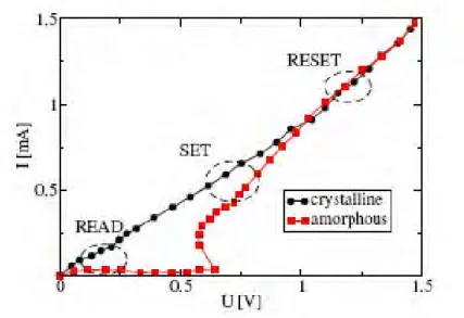
Here the write-read-erase-cycle is affected by an electrical pulse. Figs. 1-4 and 1-5 show the schematic cross section of a PCRAM cell and the corresponding current-voltage curves. The cell is essentially a nonlinear resistor and the readout is performed at low bias (Read region indicated in Fig. 1-5), where the low-field resistance changes by orders of magnitude depending on whether the phase change material in the active region of the device is crystalline or amorphous. To reach the switching regions (SET and RESET shown in Fig. 1-5) the bias is raised above the switching voltage so that enough current can flow through the cell, heating up the active region (Fig. 1-4) resulting in the crystalline-amorphous phase change [10], [11]. At present several manufacturers of RAM chips have initiated research and development projects to explore and use the potential of nonvolatile storage with phase change materials.
Although PRAM has not yet reached the commercialization stage for consumer electronic devices, nearly all prototype devices make use of a
chalcogenide alloy of germanium, antimony and tellurium (GeSbTe) called GST. It is heated to a high temperature (over 600°C), at which point the chalcogenide becomes a liquid. Once cooled, it is frozen into an amorphic glass-like state and its electrical resistance is high. By heating the chalcogenide to a temperature above its crystallization point, but below the melting point, it will transform into a crystalline state with a much lower resistance. This phase transition process can be completed in as quickly as five nanoseconds, according to a January 2006 Samsung Electronics patent application concerning the technology. This is comparable to conventional volatile memory devices, for instance, modern DRAM cells have a switching time on the order of two nanoseconds.
A more recent advance pioneered by Intel and ST Microelectronics allows the material state to be more carefully controlled, allowing it to be transformed into one of four distinct states; the previous amorphic or crystalline states, along with two new partially crystalline ones. Each of these states has different electrical properties that can be measured during reads, allowing a single cell to represent two bits, doubling memory density. [2]
VII.
Ferroelectric Random Access Memory
Ferroelectric materials are generally defined by reversible spontaneous polarization in the absence of electric field [3]. The spontaneous polarization is generated from noncentrosymmetric arrangement of ions in unit cell, which produces an electric dipole moment related to the unit cell. Adjacent unit cells are inclined to polarize in the same direction and form a region called a ferroelectric domain. Unit cell of typical ferroelectric material, ABO3, is illustrated in Fig. 1-6 [4] where A atom, B atom, and
oxygen occupy the corner site, body-centered site, and face-centered site, respectively. The ferroelectric materials exhibit a characteristic hysteresis loop as shown in Fig. 1-7 [4]. When an electrical field is applied to the ferroelectric material, the B atom, which has two thermodynamically stable positions inside oxygen octahedra, is displaced relative to the oxygens upward or downward, depending on the polarity of the electric field. This displacement generates a dipole moment inside the oxygen octahedra, which is called as saturated polarization ( ± Ps). When the applied electric
field is removed, the B atom remains in the displaced position and generates a residual polarization in the absence of applied electric field, or remanent polarization ( ± Pr). In order to reverse the direction of polarization, it needs
to apply a coercive electric field ( ± Ec), which is defined as a minimum
electric field for switching the polarization. Therefore, the basic characteristics of a ferroelectric material that make it suitable for NVM applications are its ability to retain two stable remanent polarization values at zero fields, thus providing nonvolatility. The state of polarization can be controlled and sensed by reversing the polarization from up (+1) to down (0) or vice versa as a function of applied voltage.
VIII.
Magnetoresistive Random Access Memory
In 1988, the physicists found giant magnetoresistance (GMR) effect, and from the effect they learnt the following two things. (1) Spin-dependence scattering can make a significant influence to the total resistance. (2) An interlayer coupling is quite strong between ferromagnetic layers separated by a spacing layer. Thus to investigate the interlayer couplings between ferromagnetic layers across a non-magnetic layer
becomes very interesting. One sort of the investigation is tunneling magnetoresistance (TMR) effect. TMR effect is observed on magnetic tunnel junction (MTJ). A MTJ is a layered structure of magnetic and non-magnetic materials. There are many kinds of MTJs, for instance, ferromagnet/insulator /ferromagnet trilayer junction, spin-valve-type junctions with an exchange-biased layer, double and triple barrier layers junctions and so on. Among the various structures they have a common feature that the spacing layer between the ferromagnetic layers is an insulator.
At room temperature (RT), the change of magnetoresistance in GMR is less than that in TMR, so MTJs are often used as the memory cells in MRAM. In a MTJ, the spacing layer which is an insulator is between two ferromagnetic electrodes. One electrode is free to rotate under the external field and the other creates a powerful pinning field to the magnetic layer in one specific direction.
In writing process, the magnetic moment of the free layer is rotated to be parallel or anti-parallel the pinned layer by controlling the two orthogonal magnetic fields. The resistance of the MTJ is lower when the magnetic moments of the free and pinned layer are parallel than the resistance when the moments are anti-parallel. Thus, the parallel and anti-parallel states are arbitrary chosen to present 0 or 1. In general, 0 is corresponding to the parallel state and 1 is corresponding to the anti-parallel state.
resistance is obtained to determine what the data is.
IX.
Resistive Random Access Memory
Resistive Random Access Memory (RRAM) is a new non-volatile memory type being developed by Sharp, Samsung, Fujitsu, Spansion, Macronix, Winbond and other companies.
Different forms of RRAM have been disclosed, based on different dielectric materials, spanning from perovskites to transition metal oxides to chalcogenides. Even silicon dioxide has been shown to exhibit resistive switching as early as 1967.
The basic idea is that a dielectric, which is normally insulating, can be made to conduct through a filament or conduction path formed after application of a sufficiently high voltage. The conduction path formation can arise from different mechanisms, including defects, metal migration, etc. Once the filament is formed, it may be reset (broken, resulting in high resistance) or set (re-formed, resulting in lower resistance) by an appropriately applied voltage. Recent data suggest that probably many current paths, rather than a single filament, are involved. [8]
1.2
Resistive Random Access Memory
Among new NVMs, such as SONOS, MRAM [12], FeRAM [13], PCRAM [14], and RRAM [15]-[16], RRAM shows superior advantages such as simple device structure, low operation voltage, low power consumption, long retention time, small cell size, high operation speed, low cost, good endurance, and non-destructive readout.
Its resistive switching phenomenon presents two different current values at the same applying voltage. H-state stands for higher current state and the L-state is lower state. The current states of device can be changed by applying a bias voltage or a voltage pulse. Because the resistance ratio of two current states can reach 3~5 orders of magnitude, it is easy to distinguish two current states by applying reading voltage.
1.2.1
The Structure and Operation Method of RRAM
In Fig. 1-8 [16], the RRAM is composed of a transistor and a resistor. In order to write the specific resistor to H-state, a dc voltage is applied on the word line which can turn on the bit transistor and a negative voltage pulse is applied to the bit line while the source of the transistor is grounded in Fig. 1-9 [17]. In order to erase the specific resistor to L-state, a dc voltage is also applied on the word line which can turn on the transistor and a positive voltage pulse is applied on the source of the bit transistor while the bit line is grounded. For the read operation, the word line of the memory cell is selected and a read voltage is applied on the bit line to obtain the current value while the source of the bit transistor is grounded. Therefore, the data comparing the current value with the reference value is determined and do not change the current state of the device during the read operation.
The issue of RRAM is read error. Figs. 1-10(a) and (b) [24] describe how leakage current paths make cell resistance misread. When the resistance is measured with all the unselected lines open, (3,3) cell, for example, has been changed from high to low resistance state after 3 neighboring cells are switched on because of the leakage path described in Fig. 1-10(b). Theoretically this kind of misreading and misprogramming issues can be avoided by proper biasing
method, but the amount of necessary current becomes unreasonably large as memory density increases [25]. Accordingly, it is very important to find suitable rectifying elements to realize an ultra high density cross-point memory device.
1.2.2
Material Groups of RRAM
Resistive switching behaviors have been investigated in PCRAM, doped SrZrO3 (SZO) and SrTiO3 (STO) [17]-[20], binary metal oxide, PrxCa1-xMnO
(PCMO) [21], and organic material [22], [23], and so on. The resistive switching behavior based on current-induced bistable resistance effect or voltage-controlled negative resistance phenomena has been studied in metal/insulator/metal (MIM) structure. The operation voltage of the PCRAM memory cell is large in order to change the phase between the amorphous phase and the crystalline phase. The application limitation of the PCMO device is that the resistance ratio of two current states is too small to be distinguished. In the aspect of the binary oxide materials, they are still unstable and the resistance ratio is not large enough for application. The resistance switching behaviors also have been reported in the polymer thin film, but it has drawback in stability as well as the binary oxide device.
1.3
Resistive Switching Properties of Doped SrZrO
3Films
In A. Beck’s study [16], [19], he declared that the MIM structure device manufactured with 0.2% Cr-doped SZO films as dielectric layer, SrRuO3 (SRO) and
Au as bottom and top electrode, respectively has resistive switching behavior. The previous research of our lab also uses (100)-oriented LaNiO3 (LNO) which could
enhance the preferred orientation of the SZO films to make 0.2% V-doped SZO films have resistive switching properties [26]. According to Robertsona simulation, Cr, Mn,
Fe, V, Co, Cu transition elements, which could provide over two valences in doped SZO thin films, the density of the defects could be modulated by the doping concentration. In addition, the defects are associated with different valences transformed by the applied voltage. Clearly, slight dopant concentration in SZO thin films could induce resistive switching phenomenon, and the V-doped SZO film had better resistive switching behavior. However, the effect of dopant concentration for V-doped SZO film is still unclear. This is because perovskite oxide consists of more than moments, and it’s hard to find optimal recipe to normal manufacturing process because their crystal structure and stoichiometry are hardly controllable.
From the previous research of our lab, V-doped SZO films deposited on LNO/SiO2/Si substrate have good performance in resistance switching. The resistive
switching of Al/V-doped SZO/LNO device can be operated by bias voltage and voltage pulse. However, the drawbacks of Al/V-doped SZO/LNO device are high operation voltage more than 10V.
In this thesis, the physical and electrical properties of the SZO films deposited by sputter method are reported. The SZO film is deposited on the LNO buffer layer, which is also deposited by sputter method. Pt bottom electrode is deposited on Ti/SiO2/Si substrate by electron beam evaporation method. Ti deposited by E-Gun is
acted as adhesion layer for Pt. Al is evaporated as top electrode by thermal coater. The resistive switching phenomenon can be observed in electrode/resistive thin film/buffer layer/electrode (four-layer) structure.
Four-layer structure compared with electrode/resistive thin film/electrode (tri-layer) structure could enhance the forming voltage, the switching voltage, switching speed, and improving the resistance ratio of two current states. Moreover, based on the current-voltage (I-V) curves and resistive switching phenomena, it is proposed the resistive switching mechanism is local property of SZO films. The
Fig. 1-1 Principle of operation of DRAM read (left) and write (right), for simple 4 by 4 array [5].
Fig. 1-3 Typical floating gate memory structure.
Fig. 1-4 Schematic plot of a PCRAM cell. Depending on the state of the active region (crystalline or amorphous) the resistance of the cell changes by several orders
Fig. 1-5 I-V curve of a PCRAM cell. SET and RESET denote the switching regions, while READ denotes the region of readout.
Fig. 1-7 Hysteresis loop of the ferroelectric material [4].
Fig. 1-8 Cross section schematic diagram of the RRAM. The transistor is fabricated in the front and the resistor in the back end [16].
Fig. 1-9 Equivalent circuit of an array for the write operation of a given bit resistor [17].
Chapter 2
Experiment Details
2.1
Experiment Process Flow
There are two parts of the experimental flow, including sample preparation and device property analyses as shown in Fig. 2-1. At first, we prepare the samples and make sure these samples have switching characteristics. If not, we will modify the experimental parameters and investigate the switching characteristics again until the suitable experiment parameters are obtained.
There are many steps of sample preparation as shown in Fig. 2-2. First, 4 inch boron-doped (100) silicon substrates were cleaned by standard RCA clean, and then a 200-nm-thick SiO2 layer was thermally grown on the substrates by wet oxidation
process. The SiO2 layer is acted as the isolation layer to prevent the leakage current
from the substrate. Ti deposited by electron beam evaporation is acted as adhesion layer for Pt. Then, Pt bottom electrode layer was deposited on the Ti layer also by electron beam evaporation. Synthesis of the LNO powder and the doped SZO powder were prepared previously. The powders were made to the disk-shaped target for sputtering. After that, the 100-nm-thick LNO films were deposited on the Pt bottom electrode layer to form a (100)-orientated buffer layer by radio frequency (RF) magnetron sputter. Then, the LNO buffer layer was treated by rapid temperature annealing (RTA). After that, the SZO films were deposited on the LNO buffer layer also by the RF magnetron sputter. Then, some of the SZO films were treated by rapid temperature annealing (RTA). Finally, 300-nm-thick Al top electrodes were evaporated on the SZO films by a thermal coater. The four-layer structure sample was
accomplished and the probe was detected on Al top electrode and Pt bottom electrode as shown in Fig. 2-3.
The scanning electron microscope system (SEM) and X-ray diffraction system (XRD) were used to obtain the micro-structure and the crystallization of the films, respectively. XRD analyses were helpful to confirm the orientation of the films.Field emission transmission electron microscope (FETEM) was used to analyze the interface between LNO and SZO films. Focus ion beam (FIB) was used to prepare FETEM sample. Energy dispersive X-ray analyzer (EDS) can analyze the components of LNO and SZO. An Agilent 4155C semiconductor parameter analyzer was used to record I-V curves. By the results of electrical measurement, the manufacturing process was modified to improve the performance of the device.
2.2
Radio-Frequency Magnetron Sputter Systems
In this study, a set of RF magnetron sputter system was utilized to deposit LNO and doped SZO films. The illustration of the sputter system is displayed in Fig. 2-4. The components of the sputter system are indicated as follows.
2.2.1
Vacuum System
It includes a mechanism pump and a diffusion pump. The chamber base pressure was evacuated to 10-5Torr before deposition process. There are several
valves to control the atmosphere and the pressure in the chamber and tubes.
2.2.2
Pressure System
There are two digital gauges in the system to present the chamber pressure in different working condition. One is Granville-Phlips Co.’s product with a
display range from atmosphere to 0.1 mTorr to show the higher chamber pressure for rough vacuum or sputtering condition. The other is an ion gauge with an accurate display of a high vacuum from 10-3 to 10-7 Torr. Accordingly, the vacuum situation under sputtering can be precisely controlled and the diffusion pump is working in the safe pressure.
2.2.3
Temperature Controlling System
It contains two thermal couple sensors, a set of four quartz lamps used as heater, and a temperature controller. During the heating process, the lamps just located above the wafer holder could heat the sample directly by radiation in lower pressure. At the same time, the change of the thermal couple could be detected and sent back to temperature controller to modify the heating power. Further, it could help to setup the temperature rising time, holding time, and falling time by a temperature program.
2.2.4
Gas Flow Controlling System
In general, the percentage of oxygen in the sputtering ambience plays an important role in oxide ceramics. Gas mass flow controller (MFC) is used to control the flow rate and atmosphere contents during the sputtering process. Therefore, it could find out that the dependence on the mass ratio of the device performance by tuning recipe.
2.2.5
Plasma Controlling System
This system consists of a RF power generator, a network-matching box, and a 3-inch magnetron gun. The RF power generator has only one working
frequency at 13.56MHz, and the network-matching box has minimum reflection power by adjusting the capacitance of the whole circuit. It is able to gain the stable plasma by the controlling system.
2.2.6
Cooling System
There is cooling water which flows in the pipe welded on the chamber and in the magnetron gun. During the sputtering process, the heating lamps and plasma always produce a lot of redundant heat energy in the chamber, so the cooling water is to prevent from mechanical breakdown and maintain the sample uniformity.
2.3
Preparation of Devices
In the experiment, the four-layer structure device was fabricated. The preparation flow of device is shown in Fig. 2-2.
2.3.1
Preparation of Sputter Targets
Because the LNO and SZO thin films are deposited by the sputter system, it needs two kinds of disk-shaped sputter targets, including the LNO and the doped SZO powder targets.
I.
Synthesis of the LaNiO
3Powder Target
The LNO and SZO targets are prepared by the conventional solid-state powder-mixing method. There are six steps in the synthesis processes. First, two kinds of the oxide powders, La2O3 and NiO, were mixed by the rule of
1 mol of the LNO is composed of 0.5 mol of the La2O3 and 1 mol of the
NiO. Second, the mixed powder was put into a jar with anhydrous alcohol and rolling glass balls, and then was mixed adequately by a grinder. Third, the mixture was dried by an 85oC oven. The fourth step was the sintering step. It was the most critical process, because the sintering temperature and the heating time would affect on the LNO qualities including the resistance and orientation of the LNO sputtered films. The dried mixture was put into a furnace to execute a sequence of sintering, 600oC for 2 hours and 1300oC for 10 hours. In the fifth step, the mixed powder was put in the beaker and baked it in the oven at 150oC for 2 hours. Finally, the mixed powder put in the disk-shaped target was squeezed by a high pressure of 2000 pounds for 60 seconds such that a compact target was produced for sputtering work. The preparation flow of the LNO target was showed in Fig. 2-5.
II.
Synthesis of the SrZrO
3Powder Target
The SZO powder was synthesized from two kinds of oxide powder, SrCO3 and ZrO2. In order to substitute Zr atom, it was considered the
suitable ionicradius compared with Zr atom. Considering all the conditions, transition metaloxide V2O5 was added to form the doped SZO powder.
Because V has freakyoxidation number, it could show more effect on the electric properties of our memory thin films. For example, when it is expected to synthesize 0.2 mol% V-dopedSZO powder, it should use 1 mol of SrCO3, 0.997 mol of ZrO2, and 0.00075mol of V2O5. After mixing above
elements of the doped SZO powder, the same steps were followed as synthesis of LNO powder. The mixed powder was put into a furnace of a sequence of sintering process. In the last step, a disk-shaped target was
made by a high pressure of 2000 pounds for 1 min.The manufacturing process was showed in Fig. 2-5. In this study, we prepared pure (undoped), 0.1%, 0.2%, 0.3% and 0.4% V-doped SZO powder.
2.3.2
Thin Film Depositions
The LNO bottom electrode and the doped SZO films were deposited by RF magnetron sputter sequentially. To meet our demands for different process recipe, several parameters were controlled to deposit the films based on the plasma theorem and the models of the thin film growth. There were many parameters including the chamber pressure, the RF power, the working temperature, the ambient conditions, and the deposition time. In general, chamber pressure affected the mean free path (MFP) of plasma which is relative to the deposition rate. The lower pressure was choice to create the larger MFP in the chamber, which leads to the higher deposition rate. Moreover, the deposition rate is dependent on the RF power as well. In the experiment, while depositing both the LNO and doped SZO films, the RF power was set 100 or 150W and the chamber pressure at 10 mTorr. In addition, the temperature and the ambient condition could have influence on the density of the defects, the crystallization, the conductivity, the stoichiometry, and the dielectric constant of thin films.
For the accuracy of the atmosphere, it needs the base pressure about 3×10⁻⁵ Torr before sputtering. Next, to maintain the ambient condition, the flow rate of Ar and O2 by MFC was controlled, and the working pressure was kept by the
valves among low pressure where the plasma was generated.
There were two purposes for the experiment using the RTA systems. One is in order to get stronger crystallization orientation or better conductivity of the LNO buffer layer. The other is to control the properties of our sample by changing the heating profile of RTA temperature. The RTA model was FE-004A made by JETFIRST.
2.3.4
Deposition of the Top Electrode
Before the Al top electrodes were deposited on the doped SZO films, the sample had been adhered to a metal mask. The metal mask had different hole with three kinds of diameters that are 150, 250, and 350µm. So the different areas are defined for the top electrodes, which are 1.767×10⁻⁴, 4.908×10⁻⁴, and
9.612×10⁻⁴ cm2.
Al used as the top electrode was deposition by a thermal evaporation coater (EBX-6D) manufactured by ULVAC. The samples were loaded with metal masks on the spinning holder, which made the deposition rate more uniform. Then, the rough pump and the turbo pump would work in term in order that the base pressure before deposition reached 5×10⁻⁶ Torr.
2.4
Measurements and Analyses
2.4.1
X-Ray Diffraction (XRD)
Generally, thin films are classified according to its crystallization. There are three types of crystallization, including amorphous, polycrystalline, and crystalline. XRD analysis was used to investigate the crystal structure and orientation of our sample. Furthermore, the crystallization dependence of the
samples could be identified for heat treatment. In the experiment, the thin films were grown between amorphous type and poly type. By Scherrer’s formula, 0.9 cos D B λ θ × =
× , this could estimate the average grain size from XRD illustration. Where the background information of the XRD analysis is that
λ
=1.5405Å (Kα), B is the full width at half maximum (FWHM) of the XRD peak
and θ is the diffraction angle. In this analysis, X-ray was made with 0.02 degree beam divergence and operation configuration at 30KV, 20mA.
2.4.2
Scanning Electron Microscope (SEM)
Comprehensively, the surface morphology issue is also a quite important character compared with the character of bulk for the thin films. The surface micro-morphology and cross section of our sample could be observed by SEM analysis. Besides, the crystallization of the thin films needed to be investigated directly by XRD analysis. So, SEM analysis is helpful to get enough information to support our illustration. The SEM model is S4700I with high resolution of 15Å made by Hitachi.
2.4.3
Focus Ion Beam (FIB)
FIB is a scientific instrument that resembles a scanning electron microscope. However, the SEM uses a focused beam of electrons to image the sample in the chamber, whereas a FIB instead uses a focused beam of gallium ions. Gallium is chosen because it is easy to build a gallium liquid metal ion source (LMIS). In a Gallium LMIS, gallium metal is placed in contact with a tungsten needle and heated. Gallium wets the tungsten, and a huge electric field (greater than 108V per centimeter) causes ionization and field emission of the gallium atoms.
Unlike an electron microscope, the FIB is inherently destructive to the specimen. When the high-energy gallium ions strike the sample, they will sputter atoms from the surface. Gallium atoms will also be implanted into the top few nanometers of the surface, and the surface will be made amorphous.
Because of the sputtering capability, the FIB is used as a micro-machining tool, to modify or machine materials at the micro- and nano-scale.
The FIB is commonly used to prepare samples for the transmission electron microscope. The TEM requires very thin samples, typically ~100 nanometers. The nanometer-scale resolution of the FIB allows the exact thin region to be chosen.
2.4.4
Field Emission Transmission Electron Microscope and
Energy Dispersive X-Ray Spectrometer
The state-of-the-art JEOL JEM-2100F field emission transmission electron microscope is equipped with an Oxford INCA Energy TEM 200 EDS (energy dispersive X-ray spectrometer) system, a Gatan GIF Tridiem EELS (electron energy loss spectrometer) system and a Fischione high-angle annular dark field detector. Features of the JEM-2100F include a high-brightness Schottky field emission electron gun producing a probe size of less than 0.2 nm. Ultra-high point-to-point TEM resolution is 0.19 nm; atomic scale resolution of 0.136 nm can be achieved using high angle annular dark field (HAADF) scanning transmission electron microscopy (STEM) imaging. The facilities are ideally suited for crystallographic and chemical analyses at a sub-nanometer scale, including high-sensitivity EDS and EELS.
Both EDS and EELS are analytical TEM (ATEM) techniques and can provide elemental composition and distribution information. The Oxford INCA Energy TEM 200 EDS system has the following features: automatic peak ID and labeling; element maps and linescans using SmartMap data acquisition; ability to define a line or grid of points for automatic data acquisition; absorption correction for samples of finite thickness and Sitelock image drift correction.
2.4.5
Auger Electron Microscopy (AEM)
Auger Electron Spectroscopy (
Auger spectroscopy
or AES) was developed in the late 1960's , deriving its name from the effect first observed by Pierre Auger, a French Physicist, in the mid-1920's. It is a surface specific technique utilizing the emission of low energy electrons in theAuger process
and is one of the most commonly employed surface analytical techniques for determining the composition of the surface layers of a sample.2.4.6
Secondary Ion Mass Spectrometer (SIMS)
SIMS is a technique used to analyze the composition of solid surfaces and thin films by sputtering the surface of the specimen with a focused primary ion beam and collecting and analyzing ejected secondary ions. While only charged secondary ions emitted from the material surface through the sputtering process are used to analyze the chemical composition of the material, these represent a small fraction of the particles emitted from the sample. These secondary ions are measured with a mass spectrometer to determine the elemental, isotopic, or molecular composition of the surface. SIMS is the most sensitive surface analysis technique, being able to detect elements present in the parts per billion range.
2.4.7
Current-Voltage Measurements
The most important part of all is current-voltage measurement. It could understand the electrical properties of the device from current-voltage curve. The electrical measurement system consisted of a probe station, an Agilent 4155C semiconductor parameter analyzer, an Agilent E5250A low leakage switch which are controlled by personal computer with the Agilent VEE software, and GPIB controller.
Our electrical measurements were sorted into five items, static conductivity switching measurement, retention test, stress test, endurance test, and other electrical phenomenon measurement. The aforementioned four items were tested for criteria of our memory device and the last item was executed to understand the fundamental mechanism of our samples.
I.
Static Resistive Switching Measurement
The measurement was performed by Agilent 4155C which applied a dc voltage sweeping between two specified voltages to observe the resistive switching of the sample. The measured results could observe the relation of the switching voltage and the H-state or L-state current. Use Agilent 4155C to execute the double voltage sweep function, current-voltage curve was determined with two different-current states associated with the positive applied voltage or the negative one.