國 立 交 通 大 學
電 信 工 程 學 系
碩 士 論 文
高功率低通濾波器與寬頻巴倫之設計與合成
Design and Synthesis of High-power Low-pass
Filters and Broadband Baluns
研究生:林忠傑
指導教授:張志揚 博士
高功率低通濾波器與寬頻巴倫之設計與合成
Design and Synthesis of High-power Low-pass
Filters and Broadband Baluns
研 究 生 : 林忠傑 Student : Chung-Chieh Lin
指導教授 : 張志揚 博士 Advisor : Dr. Chi-Yang Chang
國 立 交 通 大 學
電 信 工 程 學 系
碩 士 論 文
A Thesis
Submitted to Department of Communication Engineering
College of Electrical and Computer Engineering
National Chaio Tung University
In Partial Fulfillment of the Requirements
For the Degree of Master of Science
in
Communication Engineering
July 2009
Hsinchu, Taiwan, Republic of China
高功率低通濾波器與寬頻巴倫之設計與合成
研究生 : 林忠傑 指導教授 : 張志揚 博士
國 立 交 通 大 學 電 信 工 程 學 系
摘 要
本論文前半部為設計一個以集總式元件來實現的低通濾波器,因其具有高功 率規格的限制條件,故本文特別著重於材料與元件的選取,並且提出一些相關的 設計技巧和判斷條件,作為實作此高功率低通濾波器的重要依據,詳細的製作流 程和測試報告亦會在本文中討論。 本論文後半部為設計一個以高介電係數的雙面印刷電路板製程,並且使用微 帶線、槽線、共平面帶線等多種混合式的傳輸線架構來實現一個寬頻的五階巴倫 電路,此外,本文提出一個藉由理查轉換的直接精確合成方法,推導出巴倫在理 查頻域的等效電路,並且利用柴比雪夫多項式來定義完整的數學方程式,求出其 合理與可實現的聯立解,根據這個方法,我們可以任意設計所想要達成的巴倫特 性與響應參數。
Design and Synthesis of High-power Low-pass
Filters and Broadband Baluns
Student: Chung-Chieh Lin Advisor: Dr. Chi-Yang Chang
Department of Communication Engineering
National Chiao Tung University
Abstract
This thesis includes two parts. In the first part, we propose a high-power low-pass filter using all lumped components. According to the specifications of the
product, suitable choice of materials and components is the most important issue for high-power consideration. Many useful tips will be introduced to estimate the filter
performance and the detailed manufacturing process of this product will also be mentioned.
In the second part, based on the exact synthesis method by Richard’s transformation, we present a new novel broadband balun structure, which can extend
the conventional fourth-order Marchand balun to the fifth or higher order. For practical fabrication, some types of transmission-line structures can be used to
implement the network such as microstrip line (MS), slotline (SL) and coplanar stripline (CPS). Most importantly, we can arbitrarily design the parameters of balun
such as impedance transformation ratio, bandwidth and return loss by solving these established mathematical equations.
Acknowledgement
誌 謝
兩年的碩士生涯到這邊也算是圓滿的結束了,雖然時間感覺過得很快但卻也 是充滿回憶的一段快樂時光。 這篇論文的完成,首先我要感謝我的指導教授張志揚博士,在老師專業且細 心的指導下,我學習到許多關於微波領域的知識;此外,在與老師相處的過程當 中,我體會到一些不同的生活態度和人生哲學,輕鬆自在地看待每ㄧ件事情但認 真盡力地完成每ㄧ項工作,是我在未來職場與生活當中還需要努力的目標。同 時,我要感謝在口試時給予我許多寶貴建議的口試委員郭仁財教授、邱煥凱教 授、黃瑞彬教授,使本論文得以更加完善;另外,我要特別感謝中科院牛道智博 士和廖文裕先生,讓我在中科院學習到更多知識與實作的經驗。 我感到很幸運自己是這個實驗室的一員,在眾多學長姐、學弟妹以及我們9 6級同學的陪伴下,碩士生涯充滿了許多歡笑和回憶。博班學長哲慶、建育、軍 翔、金雄、正憲,95級學長姐智皓、威綸、逸亭、人錞、逸銘、獻文,97級 學弟妹揚達、姵潔、聖智、士峰,還有我們黃金96級昀緯、殿靖、耿宏、如屏, 有你們的陪伴,讓我這兩年的生活可以說是多彩多姿,回味無窮。 最後,我要感謝我最親愛的父母親、妹妹和女朋友郁涵,因為有你們的支持 和鼓勵,讓我的人生可以更加圓滿而踏實。Table of Contents
Abstract(Chinese) ... i
Abstract ... iii
Acknowledgement ... v
Table of Contents ... vii
List of Figures ... ix
List of Tables ... xiii
Chapter 1 Introduction ... 1
1.1 High-power Low-pass Filter ... 1
1.2 The Novel Marchand Balun ... 2
Chapter 2 Basic Microwave Filter Design Theory ... 5
2.1 Introduction ... 5
2.2 Filter Design Procedure ... 5
2.2.1 Power Loss Ratio Method ... 6
2.2.2 The Maximally Flat Prototype ... 7
2.2.3 The Equal-Ripple Prototype ... 9
2.3 Filter Transformation ... 11
2.3.1 Impedance and Frequency Scaling ... 12
2.3.2 High-pass Bandpass and Bandstop Transformation ... 13
Chapter 3 High-Power Low-pass Filter ... 15
3.1 Introduction ... 15
3.2 Filter Design Procedure ... 16
3.2.2 Material and Component Selection ... 19
3.3 Simulation and Measurement Comparison ... 23
3.4 Conclusion and Future Work ... 29
Chapter 4 Basic Balun Introduction ... 31
4.1 Introduction ... 31
4.2 Marchand Balun ... 32
4.2.1 Analysis and Synthesis Method ... 34
4.2.2 Chebyshev Model Establishment ... 39
4.3 Slotline ... 47
4.3.1 Slotline Analysis and Design Consideration ... 48
4.3.2 Slotline Discontinuity and Transition ... 49
Chapter 5 The Novel Marchand Balun ... 53
5.1 Introduction ... 53
5.2 Balun Design Procedure ... 54
5.2.1 The Exact Broadband Synthesis Theory ... 54
5.2.2 Mathematical Model Establishment of the Novel Balun ... 61
5.3 Simulation and Measurement Comparison ... 66
5.4 Conclusion and Future Work ... 76
List of Figures
Figure 2.1 The first four Chebyshev polynomials,TN
( )
x . ... 10Figure 2.2 Ladder circuits for low-pass filter prototypes. (a) Beginning with a series element. (b) Beginning with a shunt element. ... 11
Figure 2.3 Frequency scaling transformation. (a) Low-pass filter prototypeωC = . (b) 1 Frequency scaling. (c) Transformation to high-pass response. ... 12
Figure 2.4 Bandpass and bandstop frequency transformations. (a) Low-pass filter prototypeωC = . (b) Transformation to bandpass response. (c) Bandstop 1 response... 14
Figure 3.1 The mechanical dimmensions of the high power LPF. ... 16
Figure 3.2 The ninth-order low-pass filter prototype network... 18
Figure 3.3 The low-pass filter prototypes with different ripple-level, ... 18
Figure 3.4 The ESR of ATC-100B series. ... 20
Figure 3.5 The SMA male and N-type male connectors. ... 21
Figure 3.6 The rectangle waveguide diagram. ... 22
Figure 3.7 Product photos. (a) Vertical view with cover. (b) Lateral view with cover. (c) Vertical view without cover. (b) Lateral view without cover. ... 23
Figure 3.8 Frequency responses of Model-001. ... 24
Figure 3.9 Frequency responses of Model-002. ... 25
Figure 3.10 Broadband responses of Model-001. ... 26
Figure 3.11 Comparison between with cover and without cover of Model-001. (a) Transmission coefficient. (b) Reflection coefficient. ... 27
Figure 3.12 Power conservation check of Model-001. ... 27
Figure 4.1 Marchand compensated balun. (a) Coaxial cross section. (b) Equivalent
transmission-line model. ... 33
Figure 4.2 (a) Four-port coupled-line. (b) Its equivalent circuit. ... 35
Figure 4.3 Coupled-line Marchand balun and its equivalent circuits. ... 37
Figure 4.4 The fourth-order chebyshev filters having 5:1 bandwidth. (a) Equivalent circuit parameters. (b) Coupled-line parameters. ... 38
Figure 4.5 The equivalent circuits of Marchand baluns. (a) Second-order prototype. (b) Third-order prototype. ... 41
Figure 4.6 Normalized Chebyshev second-order prototype. (a) High-pass response. (b) Bandpass response. ... 45
Figure 4.7 Normalized Chebyshev third-order prototype. (a) High-pass response. (b) Bandpass response. ... 46
Figure 4.8 Slotline configuration ... 48
Figure 4.9 Slotline discontinuities. (a) Short-end. (b) Open-end. ... 50
Figure 4.10 Microstrip-to-slotline transition. ... 51
Figure 5.1 Mapping properties of the Richard’s transformation (a) Prototype lumped element high-pass. (b) Corresponding distributed element bandpass. ... 55
Figure 5.2 Mapping properties of the Richard’s transformation (a) Prototype lumped element low-pass. (b) Corresponding distributed element bandstop. ... 55
Figure 5.3 The fourth-order Marchand distributed and its equivalent networks. ... 56
Figure 5.4 The Chebyshev polynomials. (a) First-kind. (b) Unnormalized second-kind. (c) Normalized second-kind. ... 59
Figure 5.5 The combination type of Chebyshev polynomials. ... 60
Figure 5.6 Fifth-order distributed Marchand balun prototype. ... 61
Figure 5.7 Original two-port form of fifth-order Marchand balun. (a) Distributed prototype. (b) Richard’s domain lumped element prototype. ... 62
Figure 5.8 Equivalent circuits in S-domain. ... 64
Figure 5.9 Schematic layout of the fifth-order Marchand balun. ... 68
Figure 5.10 Practical systematic layout of the fifth-order balun withSC = j0.6. ... 69
Figure 5.11 Fabricated layout of the fifth-order balun withSC = j0.6. ... 69
Figure 5.12 Fifth-order Marchand balun responses withSC = j0.6. (a) Predicted and measured S-parameters. (b) Magnitude imbalance. (c) Phase imbalance. 71 Figure 5.13 Practical systematic layout of the fifth-order balun with SC = j0.4. ... 73
Figure 5.14 Fabricated layout of the fifth-order balun withSC = j0.4. ... 73
Figure 5.15 Fifth-order Marchand balun responses withSC = j0.4. (a) Predicted and measured S-parameters. (b) Magnitude imbalance. (c) Phase imbalance. 75 Figure 5.16 Sixth-order balun. (a) Distributed prototype. (b) Original lumped prototype. (c) Approximate responses. ... 78
List of Tables
Table 3.1 Specifications of the high-power LPF. ... 16
Table 3.2 Prototype values of ninth-order Chebyshev low-pass filter. ... 18
Table 3.3 Specifications of ATC-100B series capacitors. ... 20
Table 4.1 The ABCD parameters of some useful two-port circuits. ... 40
Table 4.2 The ABCD parameters in Richard’s domain. ... 42
Table 5.1 Theoretical prototype and circuit parameters with different cutoff frequency, 0.6 and 0.4. ( 90 @0 O f θ = and ' 1 R = ) ... 67
Table 5.2 The physical dimensions of the proposed fifth-order balun with SC = j0.6 corresponding to the layout Figure 5.10. (in mil) ... 69
Table 5.3 Comparisons for fifth-order balun with SC = j0.6 ... 72
Table 5.4 The physical dimensions of the proposed fifth-order balun with SC = j0.4 corresponding to the layout Figure 5.12. (in mil) ... 73
Chapter 1
Introduction
1.1 High-power Low-pass Filter
Modern high-performance RF filters are widely used in communication and radar transmitter systems, where there are demands of power-handling capabilities.
Since increasing power levels is the simplest way to boost system range and capability. Typical examples include satellite output filters, multiplexers and wireless diplexers.
When designing a filter for high-power operations, we often take into consideration of component breakdown and thermal condition.
RF filter is the fundamental element of the RF front of the wireless communication system. With the development of modern communication technique,
the more crowded the spectrum is, the more stringent specifications for filter design is. Consequently, high-power topic is more popular and taken seriously regarding to this
request in recent years [1]-[8].
In some applications, filters are often used to eliminate out-band interference
noises. In general, the superior filters require having steep passband-to-stopband transition, high stopband attenuation, wide stopband range and spurious resonant
frequencies far away from passband. According to the characteristic of Chebyshev polynomial, a ninth-order low-pass prototype is introduced in this paper and it is
accomplished by using purely lumped inductors and capacitors.
In chapter two, a basic microwave filter design theory will be mentioned in detail
[9]. A perfect filter would have some critical assumptions such as zero insertion loss in the passband, infinite attenuation in the stopband, and linear phase response which
can avoid signal distortion in the passband. Of course, such filters do not exist in practice, some compromises and trade-offs should be taken into account. In this
chapter, some mathematical approximating functions such as maximally flat (Butterworth) and equal-ripple (Chebyshev) prototypes will be introduced to describe
the filter responses. Based on these mathematical prototypes, the typical model for practical low-pass filter manufacture will be completely established. In addition, some
transformation theories will be introduced for other filter types in this chapter.
In chapter three, according to the specification of product, suitable choice of
materials and components is the most important issue for high-power consideration. The given specifications include insertion loss, rejection, passband VSWR, power
handling capability, temperature enduringness, connector type and box size limitation. They are all the critical conditions for design. In order to satisfy the above
specifications, we use specific materials and lumped components such as capacitors and self-made inductors to implement the high-power low-pass filter. Furthermore,
due to the high-power condition, many useful tips will be introduced to estimate the filter performance and the detailed manufacture process of this product will also be
mentioned. Finally, the related simulations, measured results and test reports are all presented in this chapter.
1.2 The Novel Marchand Balun
The word balun is an acronym for balanced-to-unbalanced transformer, used to
connect balanced transmission-line circuits to unbalanced transmission-line circuits. Balun is a key component in numerous applications such as balanced mixers,
balanced doublers, balanced frequency multipliers, balanced modulators, phase shifters, dipole feed networks and push-pull amplifiers, etc.
Balun is a three-port network, which includes an unbalanced input port and two balanced output ports. In an ideal case, it can separate the incident power into equal
portions and 180-degree phase difference. Sometimes, balun can be taken as the differential (E) port of magic-T, which is a basic but important component in many
applications [10]-[13]. Magic-T is also widely used as an element in correlation receivers, frequency discriminators, balanced mixers, four-port circulators and
reflectometers. A technique for converting balun into 180-degree hybrid by adding an in-phase power splitter is a common method [14].
Magic-T is a four-port network, which includes a sum-port (H-port), a difference-port (E-port) and two output ports. In addition, it is a bi-directional
network that allows two usage modes for different purposes. One is that when signal transmitting from sum-port or difference-port, it can split the incident power into
equal portions and in-phase or out-of-phase responses, respectively. The other mode is that it allows signals from two output ports to be summed or subtracted with relative
power and phase, then export from H-port or E-port, respectively.
Over the past half-century, several different kinds of balun structures have been
developed [15]-[17]. Early coaxial baluns were used exclusively for feeding dipole antennas. Later, planar baluns using stripline were developed for balanced mixers.
Current interest in transmission-line-type structure is focused on making it planar, compact, and more suitable for mixers and push-pull power amplifiers. In this paper,
for the purposes of flexibility, wide-band response, better performance and easy to implement, we focus on planar Marchand balun design with PCB fabrication process
[18]-[20].
In chapter four, several kinds of baluns will be mentioned briefly. Such as
coaxial baluns, planar baluns, unplanar baluns, coupled-line baluns and transmission-line baluns are all included. Most of all, Marchand balun structure
analysis is the most important and interesting topic. The basic synthesis method and mathematical model of Marchand balun will be discussed clearly in this chapter.
Besides, we also give some basic concepts and characteristics about slotline structure [21]-[26]. It is a common transmission-line structure for the hybrid type with
microstrip line to implement some practical networks.
In chapter five, based on Marchand balun theory, we present a novel broadband
balun structure, which can extend the conventional fourth-order Marchand balun to the fifth or higher order. For practical fabrication, some types of transmission-line
structures can be used to implement the fifth-order Marchand balun such as microstrip line (MS), slotline (SL) and coplanar stripline (CPS). Due to the entire network is
composed of transmission-lines and stubs with identical electrical length, the exact synthesis method by Richard’s transformation can be used to derive the complete
mathematical model of the presented novel balun [27]-[32]. We can arbitrarily design the parameters of balun such as impedance transformation ratio, bandwidth and return
loss by solving these mathematical equations.
Both of the high-power low-pass filter and novel Marchand balun network, the
complete circuit analyses, design procedures, simulations and measured results will be discussed in this paper.
Chapter 2
Basic Microwave Filter Design Theory
2.1 Introduction
A microwave filter is a two-port network used to control the frequency response for many different designers. It provides transmission at frequencies within the
passband and attenuation in the stopband of the filter. Typical frequency responses include low-pass, high-pass, basspass and bandstop characteristics. Nowadays, there
are many applications of microwave communication, radar or other test and measurement system.
In this chapter, we will introduce the modern procedure called the insertion loss method [8], [9]. It uses network synthesis techniques to design filters with a
completely specified frequency responses. In general, the design begins with low-pass filter prototype. The common mathematical approximations such as maximally flat
(Butterworth) and equal-ripple (Chebyshev) polynomials are often used to describe the filter responses. In addition, we can convert the basic low-pass prototype to other
particular frequency range and impedance level by using some transformation rules.
2.2 Filter Design Procedure
The perfect filter responses would have zero insertion loss in the passband, infinite attenuation in the stopband and a linear phase response in the passband. But
such filter does not exist in practical, so we should make some compromises in our design. Both of lumped or distributed realization can be used to implement the
The insertion loss method is a systematic way to synthesis desired responses of filters. It allows a high degree of control over the passband and stopband amplitude
and phase characteristics. According to the design procedure, we can easily evaluate the design trade-offs to best meet the application requirements. For non-periodic
implementation purpose, we will focus on the establishment of lumped element prototype.
2.2.1 Power Loss Ratio Method
First, we define the analysis method based on reciprocal and lossless network conditions. For two-port networks, it is known that impedance and admittance
matrices are symmetric for reciprocal networks and purely imaginary for lossless networks. Similarly, the scattering matrix which is the common parameter we use to
describe network characteristics has its special properties. It is symmetric for reciprocal networks and unitary for lossless networks. A matrix that satisfies the
conditions of Equation (2.1) and (2.2) is called symmetric matrix or unitary matrix, respectively.
[ ] [ ]
t S = S(2.1)
[ ] [ ]
*{ }
t 1 S S − = (2.2) Assume that the low-pass prototype is a passive, reciprocal and lossless two-port network. Based on these assumptions in power loss ratio method, a filter can bewell-defined by its insertion loss or power loss ratio, denotes PLR:
2 1 1 ( ) inc LR load P Power available from source P
Power delivered to load P ω
= = =
− Γ
(2.3)
, where ( )Γ ω represents the reflection coefficient of the network. In symmetric two-port network, we can use S11 or S22 denotation to describe it. The insertion loss
(IL) function in dB is defined as
10
10log LR
IL= P (2.4) , and the S11 and S21 parameter is also defined as
2 11 1 1 LR S P = − (2.5) 2 21 1 LR S P = (2.6) We know that Γ( )ω 2 is an even function of ω , therefore it can be expressed as a polynomial in ω2. Thus we can write
2 2 2 2 ( ) ( ) ( ) ( ) M M N ω ω ω ω Γ = + (2.7)
, where M and N are all real polynomials in ω2. Substituting this form in equation
(2.3) gives the following form.
2 2 ( ) 1 ( ) LR M P N ω ω = +
(2.8)
Thus, we certainly define the standard form for filter design purpose in power loss ratio formula. Next, some common mathematical polynomials combined with the
power loss ratio formula can be used to describe the practical low-pass filter responses. Moreover, it is easy to convert the typical low-pass prototype into a
bandpass or other filter types by using various transformation rules.
2.2.2 The Maximally Flat Prototype
The maximally flat approximation, which is also called the Butterworth or
binomial response, is the simplest meaningful approximation to describe a practical low-pass filter. It provides the flattest possible passband response, better group delay
performance but worse selectivity. For low-pass filter prototype, it is specified as follow.
2 2 1 ( ) N LR C P ε ω ω = +
(2.9)
, where N represents the order and ωC is the cut-off frequency of the filter. In
general, ωC is equal to unity in an original normalized prototype. The range of filter passband is defined from ω=0 to ω ω= C and the power loss ratio is equal to
2
1+ε at the band edge. In addation, we often choose the proper ripple-level value to make PLR in -3dB point. It is means that half of power reflects back to the input port when ε =1. Like the binomial response for multi-section quarter-wave matching transformer, the first (2N-1) derivatives of power loss ratio are zero at ω =0. The mathematical approximation implies a very flat response across the passband. The
squared S21-magnitude is also defined in Equation (2.10).
2 21 2 1 ( ) 1 ( ) N C S ω ω ω = + (2.10) It is important to calculate the degree N of the filter in order to meet a given
specifications. First, we introduce two parameters for calculating the required return loss and insertion loss which denote LR and LA, respectively.
2 10 10log (1 N) A L = +ω (2.11) 2 10 2 1 10log ( ) N R N L ω ω + = (2.12) , then we check the following two inequalities.
R p
return loss≥L for ω ω≤ (2.13)
A s
insertion loss≥L for ω ω≥ (2.14) , where ωp and ωs represent the passband and stopband frequencies, respectively.
The ratio of stopband to passband denotes S, which is defined in Equation (2.15) as follow.
1 s p S ω ω = ≥ (2.15) Finally, an inequality to decide the necessary degree N of the Butterworth prototype filter can be derived as
10 20log ( ) A R L L N S + ≥ (2.16)
2.2.3 The Equal-Ripple Prototype
The equal-ripple approximation, which is also called Chebyshev response, is another common approximation to filter design. Although the flatness of in-band
response and group delay performance are worse than the Butterworth response, it has a sharper out-band selectivity and provides fewer elements for necessary rejection
response of filter. For low-pass filter prototype, it can be specified as following function. 2 2 1 ( ) LR N C P ε T ω ω = +
(2.17)
, where N represents the order and ωC is the cut-off frequency of the filter. Different
from Butterworth approximation, it introduces a parameter ε2 which determines the
passband ripple-level. There are Chebyshev polynomials denote TN(x) defined as follows.
( )
( )
( )
( )
0 1 2 2 3 3 1 2 1 4 3 T x T x x T x x T x x x = = = − = − (2.18)Equation (2.18) gives the first four Chebyshev polynomials and the higher-order polynomials can be found by using the following recurrence formula.
( )
2 1( )
2( )
N N N
T x = xT − x −T − x (2.19)
several significant properties of Chebyshev polynomial expressed.
(1.) For − ≤ ≤1 x 1, TN
( )
x ≤ . Chebyshev polynomials oscillate between ±1 in 1this range. This is the most important property of the equal-ripple characteristic and
the region will be mapped to the passband of the low-pass filter.
(2.) For x >1, TN
( )
x > . This region will be mapped to the range outside the 1passband of the low-pass filter.
(3.) For x >1, TN
( )
x increases faster with x as N increases.Figure 2.1 The first four Chebyshev polynomials,TN
( )
x .Similar as the Butterworth approximation analysis procedures, the squared
S21-magnitude of Chebyshev approximation is defined as
2 21 2 2 1 ( ) 1 N( ) C S T ω ω ε ω = + (2.20) The proper degree resolution of Chebyshev approximation is expressed as follow.
2 1 2 10 6 20log [ ( 1) ] A R L L N S S + + ≥ + − (2.21)
In this chapter, ladder circuit model is used to construct low-pass filter prototype for both Butterworth and Chebyshev approximations. In a normalized low-pass
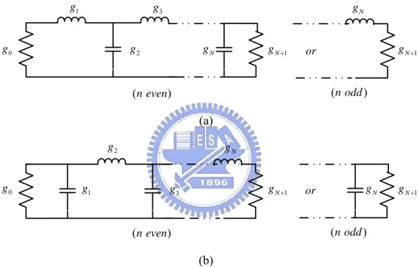
prototype where the source impedance and the cutoff frequency are normalized to unity, we can arbitrarily determine the filter degree and ripple-level to achieve the complete normalized element values denote g . Figure 2.2 shows different kinds of S
N-degree ladder networks and element values are numbered from g to 0 gN+1.
0 g 3 g 2 g 1 g 1 N g + N g or gN+1 N g ( )n even ( )n odd (a) 0 g g1 g3 2 g 1 N g + N g or gN gN+1 ( )n even ( )n odd (b)
Figure 2.2 Ladder circuits for low-pass filter prototypes. (a) Beginning with a series
element. (b) Beginning with a shunt element.
2.3 Filter Transformation
Low-pass filter is the most important component we are concerned about in filter
design. Based on the basic low-pass prototype, the other types of filter design procedures are also summarized in this section. The high-pass, bandpass and bandstop
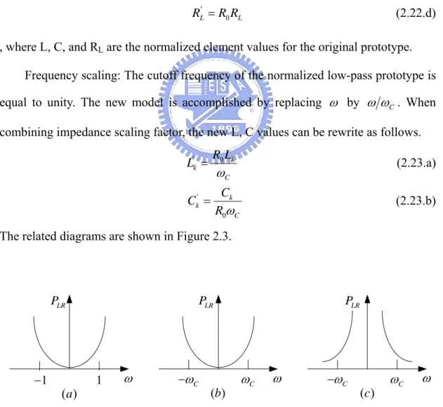
2.3.1 Impedance and Frequency Scaling
Impedance scaling: In the previously low-pass prototype design, the source and
load resistances are set to unity except the Chebyshev prototype network with even degree. Supposed that source resistance scale to R and the new filter component 0
values are given by
' 0 L =R L (2.22.a) ' 0 C C R = (2.22.b) ' 0 S R =R (2.22.c) ' 0 L L R =R R (2.22.d) , where L, C, and RL are the normalized element values for the original prototype.
Frequency scaling: The cutoff frequency of the normalized low-pass prototype is equal to unity. The new model is accomplished by replacing ω by ω ωC. When combining impedance scaling factor, the new L, C values can be rewrite as follows.
' 0 k k C R L L ω = (2.23.a) ' 0 k k C C C Rω = (2.23.b) The related diagrams are shown in Figure 2.3.
LR P LR P PLR ω ω ω −ωC ωC −ωC ωC 1 1 − ( )a ( )b ( )c
Figure 2.3 Frequency scaling transformation. (a) Low-pass filter prototypeωC = . (b) 1 Frequency scaling. (c) Transformation to high-pass response.
2.3.2 High-pass Bandpass and Bandstop Transformation
High-pass transformation: We can use the following substitution to convert a
low-pass response to a high-pass response.
C
ω ω
ω
← − (2.24) It maps ω =0 to ω= ±∞ , and vice versa. The cutoff frequency occurs when
C
ω= ±ω . The negative sign is necessary to convert inductors (capacitors) to realizable capacitors (inductors).
Bandpass transformation: Low-pass prototype is also transformed to bandpass response by replacing the frequency ω . Similarly, there is a mathematical substitution for this transformation as shown in Equation (2.25).
0 0 0 2 1 0 0 1 ( ) ( ) ω ω ω ω ω ω ω ω ω ω ω ω ← − = − − ∆ (2.25) , where ω0 is the center frequency; ω1 and ω2 denote the edges of the passband;
∆
is the fractional bandwidth (FBW) of the bandpass filter defined in Equation (2.26). 2 1 0 ω ω ω − ∆ = (2.26) Bandstop transformation: The inverse transformation can be used to obtain a bandstop response. Substitution is shown below.1 0 0 (ω ω ) ω ω ω − ← −∆ − (2.27) The related diagrams are shown in Figure 2.4.
LR P LR P PLR ω ω ω 0 ω ω0 0 ω − −ω0 1 1 − ( )a ( )b ( )c 2 ω − −ω1 ω1 ω2 −ω2 −ω1 ω1 ω2 Figure 2.4 Bandpass and bandstop frequency transformations. (a) Low-pass filter prototypeωC = . (b) Transformation to bandpass response. (c) Bandstop response. 1
Chapter 3
High-Power Low-pass Filter
3.1 Introduction
In modern science and technology, to pursue faster, wider system usage range,
more efficient capability and more accurate performance, the high-power topic is deeply concerned [1]-[7]. Not only in academic researches, it becomes more popular
in some business applications. More and more companies endeavor to invent new products in this area. For example, satellite output filters and multiplexers, wireless or
radio base station transmitter filters and diplexers, etc.
Due to the high market demands for volume and mass production, there are more
and more challenges in high-power operations. When designing a filter for these high-power requirements, there exist many effects which must be taken into account.
For examples, multipaction breakdown, ionization breakdown, passive inter-modulation (PIM) interferences and thermal-related high-power breakdown are
all the possible phenomena in this field [7].
The presented high-power low-pass filter will be applied to the output stage of a
communication system. The circuit prior to this filter is a power amplifier used to increase the intensity of output signals. However, it could increase the harmonic
noises as well, so the low-pass filter is necessary used to suppress these harmonic noises which are produced from the power amplifier. Therefore, the power-resistant
and high-temperature-resistant characteristics are stressed significantly in this product.
about 100 to 150Watts. Compared to other higher power level applications, the thermal-related venting mechanism is the most important topic in this design. In
following sections, complete design procedures and comparison between simulations and measured results are presented.
3.2 Filter Design Procedure
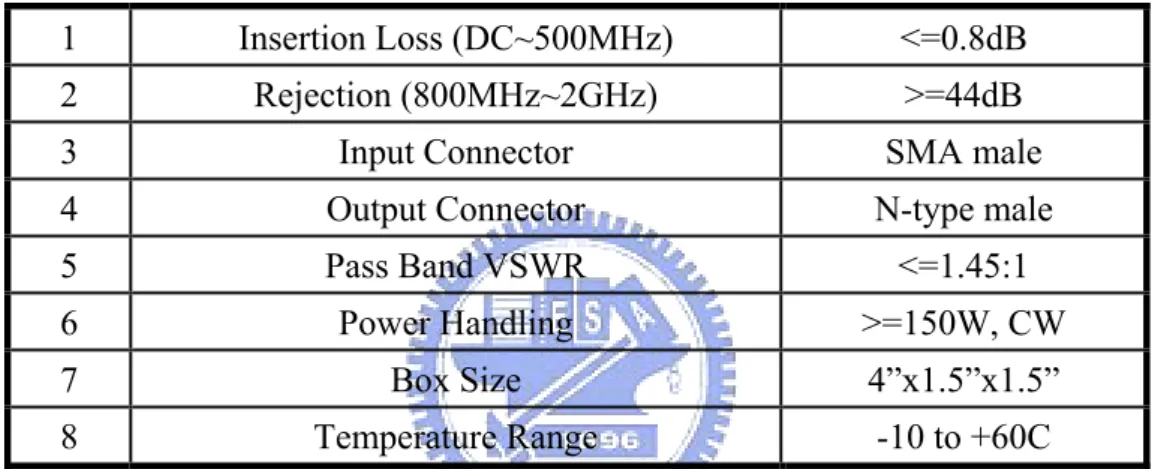
For the given high-power low-pass filter specifications, listed in Table 3.1.
1 Insertion Loss (DC~500MHz) <=0.8dB
2 Rejection (800MHz~2GHz) >=44dB
3 Input Connector SMA male
4 Output Connector N-type male
5 Pass Band VSWR <=1.45:1
6 Power Handling >=150W, CW
7 Box Size 4”x1.5”x1.5”
8 Temperature Range -10 to +60C
Table 3.1 Specifications of the high-power LPF.
The filter box mechanical drawing is shown in Figure 3.1.
3.2.1 Prototype Establishment
First, we must determine the appropriate low-pass response model which can
conform to the given specifications such as insertion loss, rejection and passband VSWR. For the practical implementation consideration, we use ladder network
prototype which is beginning with a series inductor shown in Figure 2.2(a). In addition, an odd-order low-pass filter model is constructed for a symmetric structure.
In this chapter, we give a moderate design model by using Chebyshev polynomial approximation. It provides better design sense about response selectivity and less
volume consumption of practical product.
The Equation (2.21) introduced last chapter can be used to determine an
appropriate degree for the proposed low-pass filter. The related specifications include passband insertion loss, stopband rejection, passband VSWR and the ratio of stopband
to passband, denotes S. The Equation (3.1) gives the relationship between VSWR and reflection coefficient, S11. 11 max min 11 1 1 S V VSWR V S + = = − (3.1) According to the given VSWR value, S11 is well determined and equal to
-14.719dB. In other words, we choose the proper value of LR which is equal to
15dB. We obtain N ≥7.147 by means of the known parameters such as LA, ωs
and ωp. So, the least filter degree is easily determined by (2.21) and it is chosen to a
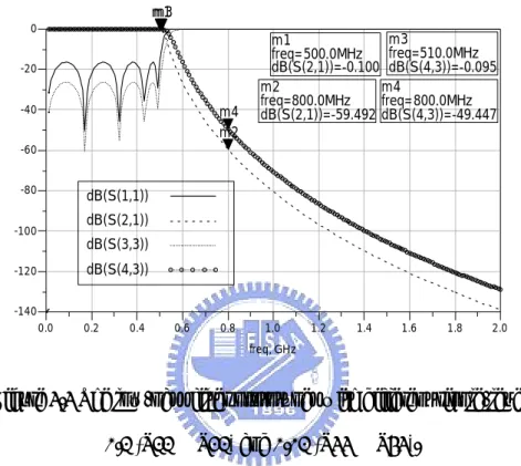
ninth-order model. The ladder network is plotted in Figure 3.2.
Second, for the sake of the given passband insertion loss limitation, we choose
the proper ripple-level model to analyze the filter. There are two models with different ripple-levels as shown in Figure 3.3. The ripple values are ε =0.1 and ε =0.01, respectively.
Figure 3.2 The ninth-order low-pass filter prototype network. 0.2 0.4 0.6 0.8 1.0 1.2 1.4 1.6 1.8 0.0 2.0 -120 -100 -80 -60 -40 -20 -140 0 freq, GHz m1 m2 m3 m4 m1 freq= dB(S(2,1))=-0.100500.0MHz m2 freq= dB(S(2,1))=-59.492800.0MHz m3 freq= dB(S(4,3))=-0.095510.0MHz m4 freq= dB(S(4,3))=-49.447800.0MHz dB(S(1,1)) dB(S(2,1)) dB(S(3,3)) dB(S(4,3))
Figure 3.3 The low-pass filter prototypes with different ripple-level,
0.1 (S11 & S21) and 0.01 (S33 & S43).
Comparing the responses of two different ripple-levels, it is observed that the larger ripple-level we choose, the better out-band selectivity but the worse passband
return loss level. Therefore, we should consider a moderate and reasonable choice in our design seriously. Finally, the ninth-order Chebyshev low-pass filter prototype with ripple-levelε =0.01 is accomplished. The detailed prototype component values of Figure 3.2 are listed in Table 3.2.
L1/L5 (nH) L2/L4 (nH) L3(nH) C1/C4 (pF) C2/C3 (pF) 12.962 28.717 30.331 9.084 10.902 Table 3.2 Prototype values of ninth-order Chebyshev low-pass filter.
3.2.2 Material and Component Selection
Now, the reasonable model has been well determined for our design. Next, we
will select suitable materials and components to implement it. In a lumped circuit filter, capacitors and inductors are the essential and fundamental components. The
choice of superior lumped elements is one of the major issues about filter implementation. For high-power condition, the strong and good heat-venting
materials and components are preferred to use. Later, some useful tips are introduced for achieving better filter performance and endurance.
According to these following steps, the summary estimations of capacitors are presented.
(1.) First, we should estimate the electric potential across each shunt capacitor. We suppose the maximal input power of detection is about 200Watts and the network
is set up on 50Ω-system. From simple electrical power equation, the r.m.s. value of electric potential is equal to 100Volts, which represents the reference withstanding
voltage. Consequently, the suitable capacitors will be chosen based on this reference value.
(2.) Second, we calculate the 10pF capacitor impedance around the passband edge, about 500MHz. From the following equation, X is easily obtained. C
6 12 1 1 31.83 2 2 500 10 10 10 C X fC π π − = = = Ω ⋅ ⋅ ⋅ ⋅ (3.2) (3.) When V and X are determined, we can also estimate the r.m.s. value of C
current across capacitors. From (1.) and (2.), we obtain the reference withstanding current Irms flowing through the capacitor which is equal to 3.1416 Amps.
According to this simple analysis, we choose ATC-100B-Porcelain-Superchip
-Multilayer-Capacitors to implement the filter. This kind of capacitors has many product attributes such as high-Q, low noise, high self-resonance, low ESR/ESL and
ultra-stable performance characteristics. The basic specifications about the ATC-100B series are listed in Table 3.3. Especially, the WVDC parameter of capacitors conforms
to the reference withstanding voltage we calculate before.
1 Capacitance Range 0.1~1000pF
2 High Q >=10000 @ 1MHz
3 DC Working Voltage (WVDC) 500V @ 0.1~100pF
4 Temperature Coefficient (TCC) +90 +/- 20ppm/oC @ -55oC to +125oC +90 +/- 30ppm/oC @ +125oC to +175oC Table 3.3 Specifications of ATC-100B series capacitors.
(4.) Finally, according to the estimated Irms and given ESR value plotted in
Figure 3.4, we can calculate the power loss ratio of each shunt capacitor. The complete calculations are given by
2 3.14162 0.1 0.98( )
L rms
P =I ×ESR= × ≈ watt (3.3.a) 0.98 0.49% 200 L T P P = = (3.3.b)
Figure 3.4 The ESR of ATC-100B series.
The larger degree the filter is, the more the power loses. Another clever tip is the arrangement of capacitors. We can erect two or three shunt capacitors to achieve
shunt stage includes three capacitors. In the Figure 3.2, C1 and C4 are composed of 2pF (2R0BW), 2.2pF (2R2BW) and 4.7pF (4R7CW) capacitors; C2 and C3 are
composed of 1.5pF (1R5BW), 2pF (2R0BW) and 6.8pF (6R8CW) capacitors.
To obtain arbitrary inductances for our design, we use the self-made inductors.
For the sake of convenience on fabrication and the high-power-resistant features, the inductors are made of the semi-rigid coaxial cable with a 0,034” outside diameter,
which is a 50-Ohm-Semi-Rigid Coaxial-Line from JYEBAO Corp. in Taipei Hsien, Taiwan. Then, we use the impedance analyzer, HP/Agilent 4191A RF Impedance
Analyzer with frequency ranging from 1 to 1000 MHz, to measure the accurate capacitance and inductance around the design cutoff frequency. According to
measuring experience, the half-turn of an inductor is about 10~15nH and a three-turn inductor is about 25~30nH. The inductances can be adjusted to fit the ideal prototype
responses by tuning the space at intervals of spiral inductors.
The last considerations are connector choice and box design. From specifications,
we buy the proper 50Ω SMA-male and N-type-male connectors from JYEBAO Corp. The related connector configurations are shown in Figure 3.5.
The box is an aluminum 6061-T6 material fabricated by machining which is plated with silver for possible soldering of capacitors and low loss. The metal housing,
on the one part, provides better heat-venting efficiency and, on the other part, provides better isolation characteristic as well as to avoid the parasitic short-circuited
effect. We can use basic concept of rectangle waveguide to estimate the cutoff frequency, which occurs in the aperture between cavities. The related rectangular
waveguide is shown in Figure 3.6. The cutoff frequencies of the rectangular waveguide with width a and height b is
2 2 1 ( ) 2 C mn m n f a b µε = + (3.4)
, where ( )fC mn is the cutoff frequency of the rectangular waveguide at aperture
region. That is, EM wave with a frequency higher than the lowest cutoff frequency
(TE10 mode, ie. m=1, n=0) can propagate in the waveguide. Otherwise, it will be a evanescent decayed wave. In this case, the first two dominant modes are
10 18.69
TE ≈ GHz and TM11≈26.43GHz . They are all much higher than the frequency range we are interested.
3.3 Simulation and Measurement Comparison
The implemented product photos are shown in Figure 3.7, including both the vertical and lateral view. In these photos, we can clearly observe that the ninth-order
low-pass filter arrangement and box structure. The mechanical design divides the whole cavity into five small cavities to push the cavity resonance to a much higher
frequency. If the cavity resonant frequency occurs inside or near the filter passabnd, the filter performance may be degraded. To solve this problem, we separate the each
cavity by metal wall and it can shift the resonance to higher frequency effectively.
(a) (b)
(c) (d)
Figure 3.7 Product photos. (a)Vertical view with cover. (b)Lateral view with cover. (c)Vertical view without cover. (b)Lateral view without cover.
There are four samples of the high-power low-pass filters being fabricated. In this paper, we present only two samples (S/N:-001/-002). The measured frequency
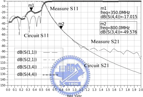
responses which include the model-001 and model-002 are shown in Figure 3.8 and Figure 3.9. 0.1 0.2 0.3 0.4 0.5 0.6 0.7 0.8 0.9 1.0 1.1 1.2 1.3 1.4 1.5 1.6 1.7 1.8 1.9 0.0 2.0 -140 -130 -120 -110 -100 -90 -80 -70 -60 -50 -40 -30 -20 -10 -150 0 freq, GHz m2 m1 dB(S(1,1)) dB(S(2,1)) dB(S(3,4)) dB(S(4,4)) m1 freq= dB(S(4,4))=-17.015350.0MHz m2 freq= dB(S(3,4))=-49.576800.0MHz 50 100 150 200 250 300 350 400 450 0 500 -0.8 -0.6 -0.4 -0.2 0.0 -1.0 0.2 freq, MHz dB(S(2,1)) dB(S(3,4))
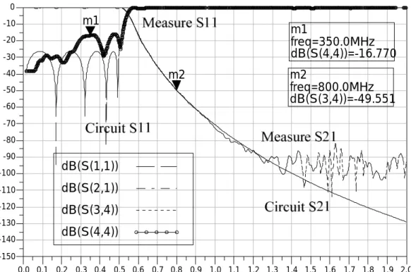
0.1 0.2 0.3 0.4 0.5 0.6 0.7 0.8 0.9 1.0 1.1 1.2 1.3 1.4 1.5 1.6 1.7 1.8 1.9 0.0 2.0 -140 -130 -120 -110 -100 -90 -80 -70 -60 -50 -40 -30 -20 -10 -150 0 freq, GHz m2 m1 m2 freq= dB(S(3,4))=-49.551800.0MHz m1 freq= dB(S(4,4))=-16.770350.0MHz dB(S(1,1)) dB(S(2,1)) dB(S(3,4)) dB(S(4,4)) 50 100 150 200 250 300 350 400 450 0 500 -0.8 -0.6 -0.4 -0.2 0.0 -1.0 0.2 freq, MHz dB(S(2,1)) dB(S(3,4))
Figure 3.9 Frequency responses of Model-002.
From the measured results, the passband (DC~500MHz) return loss and stopband (800MHz~2GHz) rejection all conform to the specifications. They are below
16.5dB and 49.5dB, respectively.
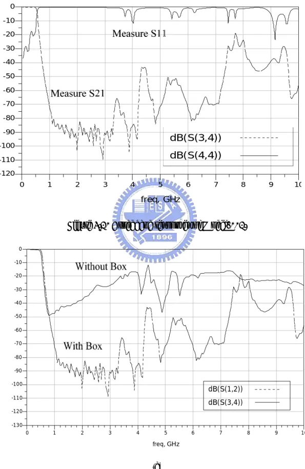
comparison to the filter without cover in Figure 3.11 and Figure 3.12. 1 2 3 4 5 6 7 8 9 0 10 -110 -100 -90 -80 -70 -60 -50 -40 -30 -20 -10 -120 0 freq, GHz dB(S(3,4)) dB(S(4,4))
Figure 3.10 Broadband responses of Model-001.
1 2 3 4 5 6 7 8 9 0 10 -120 -110 -100 -90 -80 -70 -60 -50 -40 -30 -20 -10 -130 0 freq, GHz dB(S(1,2)) dB(S(3,4)) (a)
0.1 0.2 0.3 0.4 0.5 0.6 0.7 0.8 0.9 0.0 1.0 -35 -30 -25 -20 -15 -10 -5 -40 0 freq, GHz dB(S(1,1)) dB(S(3,3)) (b)
Figure 3.11 Comparison between with cover and without cover of Model-001. (a)
Transmission coefficient. (b) Reflection coefficient.
1 2 3 4 5 6 7 8 9 0 10 0.2 0.4 0.6 0.8 0.0 1.0 freq, GHz sqr(mag(S(1,1)))+sqr(mag(S(2,1))) sqr(mag(S(3,3)))+sqr(mag(S(4,3)))
The measured frequency range is from 50MHz to 10GHz. In Figure 3.10, the box resonances occur at the high frequencies such as 4.4GHz, 5.6GHz, 7.6GHz and
9.4GHz. Because of the radiation loss at these frequencies, the transmission coefficients are not satisfied the -40dB level. The differences between the filter with
cover and without cover are shown clearly in Figure 3.11 and Figure 3.12. The detailed discussions and concepts are mentioned below.
(1.) There exist some noises propagating in free space. When inductor is exposed outside, it may couple with other power like an antenna. Because cover can give good
isolation between inductors and outside noises, the insertion loss of filter with cover is better than the without one above 1GHz.
(2) Due to the coupling and parasitic effect, it will change the inductances we measured. Therefore, it may lead to slightly frequency response distortion.
(3.) Figure 3.12 shows the power conservation result. The dot-line response represents the filter with cover is better than the solid-line response which has no
cover.
Finally, the high-power detection report is expressed in Figure 3.13. For
protection reason, it is necessary that the -40dBm attenuator device is added in front of power meter. There is a dBm calculation equation as shown below.
10
10log ( / 0.001 )
dBm= P Watt (3.5) To achieve 100Watts power, the detected value from power meter is must equal to
10dBm. From the measured report shown in Figure 3.13, both two models have good high-power-resistant property and their insertion differences are all below 1dBm from
Freq.(MHz) 400 410 420 430 440 450 460 470 480 490 500 L Di ff.(dBm) (Without LPF-With LPF) 0.2 0.4 0.6 0.8 1.0 MODEL-001 MODEL-002 Figure 3.13 High-power detection report of Model-001/-002.
3.4 Conclusion and Future Work
High-power studies of a filter are the latest and popular topic. Most of all, looking for proper materials and components is the key point to implement the better
designs. The basic specifications and characteristics of specific components can be well defined by using full-wave EM simulation tools and it provides better and faster
design sense to network implementation. Besides some high-power effects mentioned before, there are some practical issues such as the multicarrier operation, sharp edge
condition, design margin and prevention techniques are also covered. In this paper, low-pass filter is the most interesting design we focus on. The steeper selectivity and
better stopband rejection performance will be obtained by introducing the transmission zeros by general Chebyshev polynomial form [33, 34]. In addition,
according to the transformation methods in chapter two, some applications such as high-pass filters, bandpass filters, diplexers and multiplexers can be achieved [35, 36].
Chapter 4
Basic Balun Introduction
4.1 Introduction
With the recent growth in the telecommunication area, the demands for smaller, faster and more reliable device design and fabrication of circuits have been increasing.
Passive components play just as an important role as active devices in satisfying these requirements. In addition, great interest has been aroused from both academic and
industrial areas toward wide-band technology. As a key component in wide-band wireless communication system, balun with high performance, compact size and low
cost are highly demanded [14]-[20].
A balun is a device intended to act as a transformer which is matching an
unbalanced circuit to a balanced one, or vice versa. A large number of analog radio frequency (RF) and microwave circuits require balanced inputs and outputs in order to
reduce noises and high-order harmonics as well as improve dynamic range of circuits. It is a key component in many wireless communication systems for realizing critical
building blocks such as balanced mixers, balanced doublers, balanced frequency multipliers, balanced modulators, phase shifters, push-pull amplifiers and dipole
antenna feeding networks.
Various balun configurations have been reported for many applications in
microwave integrated circuits (MICs) and microwave monolithic integrated circuits (MMICs). Several kinds of balun structures have been developed over the pass
half-century such as coaxial baluns, unplanar baluns and planar baluns. Among them, the planar version of the Marchand balun is perhaps one of the most attractive baluns
due to its planar structure and wide-band performance [18, 19]. Furthermore, the multi-section half-wave or quarter-wave baluns are frequently used in microwave
circuits as they can easily be realized with various design procedures and fabrication processes. They also provide satisfactory performances, namely, small insertion loss,
low voltage standing wave ratio (VSWR) and good amplitude/phase imbalance between two balanced ports. In this chapter, because of the practical consideration of
implementation, we also discuss some basic concepts and characteristics about slotline transmission-line structure [21]-[26].
4.2 Marchand Balun
Current interest balun design is focused toward making it planar, compact and
broadband performance. In an ideal case, it can separate the incident power into equal portions and 180-degree phase difference responses. Due to the broadband
performance and simplicity of implementation, planar Marchand balun is the most popular design choice in recent years. In this chapter, the related theories and analyses
of Marchand balun are presented [18]-[20].
The first transmission-line balun was described in the literature by Lindenbald in
1939 and variations based on his original scheme soon followed. Among these was Marchand, who introduced a series open-circuited line to compensate for the
short-circuited line reactance. In coupled-line balun design, as compared with a short coupled-line one, Marchand structure has less stringent requirements for Zoe ,
generally 3 ~ 5Zoe ≈ Zoo is sufficient to obtain good performance. There is Marchand
L
Z
2 SZ
1 SZ
a b 0Z
1Z
2Z
BZ
Housing
(a) 2Z
2 SZ
BZ
1 SZ
1Z
Z
L 0Z
a
b
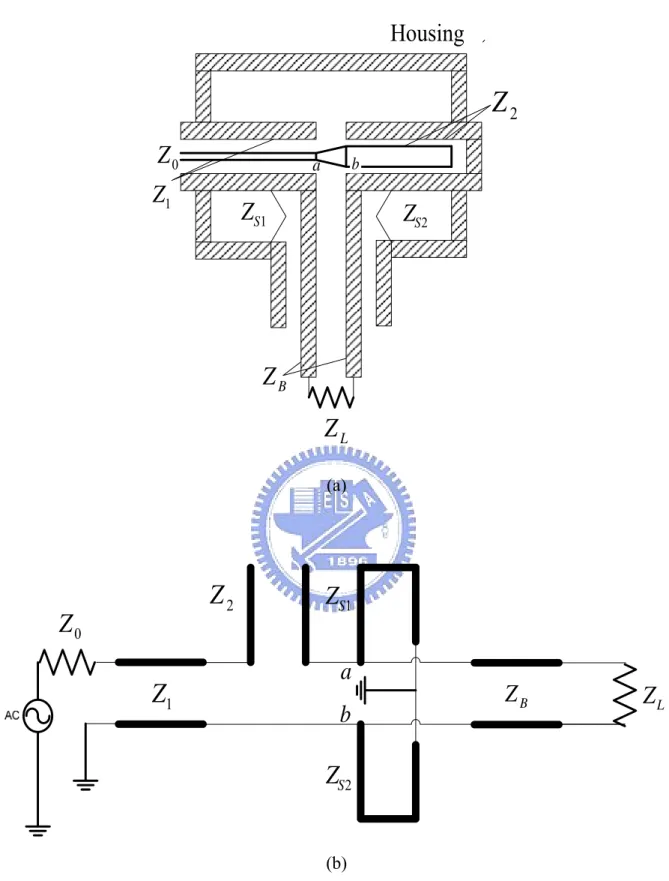
(b)Figure 4.1 Marchand compensated balun. (a) Coaxial cross section. (b) Equivalent transmission-line model.
The compensated coaxial balun [17] basically consists of an unbalanced (Z1), an open-circuited (Z2), two short-circuited (ZS1 and ZS2) and balanced (ZB)
transmission-line sections. Each section is about a quarter-wavelength long at the center frequency of operation. As shown in Figure 4.1(b), the open-circuited stub and
short-circuited stubs are in series and shunt connection to the balanced line, respectively. Most of all, the ratio of the characteristic impedances of short-circuited
and open-circuited stubs determines the bandwidth. In general, the higher the ratio is, the wider the bandwidth is. This is the basic but important concept to evaluate
bandwidth of Marchand balun. In later design, choosing the proper transmission-line types is also a major issue.
4.2.1 Analysis and Synthesis Method
A Marchand balun can easily be realized by using a pair of coupled lines as shown in Figure 4.2 [8]. We can design a planar balun to meet the desired responses
by properly selecting its parameters. First, the coupled-line type of Marchand balun will be presented. According to this equivalent model, we will use Richard’s
transformation method to establish the reasonable solutions of second-order and third-order Marchand balun. In this chapter, the Chebyshev polynomial is chosen as
the mathematical model for design a definable Marchand balun. The complete design procedures and calculating processes will be introduced in detail in later chapter.
Synthesis techniques of such baluns have been recently described and summarized in this section. A four-port coupled-line and its equivalent circuit are
, (
oe,
oo)
k Z Z
Z
1
2
3
4
Z
2 1Z
1
2
3
4
:1
N
1: N
( )
a
( )
b
Figure 4.2 (a) Four-port coupled-line. (b) Its equivalent circuit.
, where Z1 and Z2 are the characteristic impedances of distributed unit elements; N is the transformer turns ratio. The relationship between Zoc and the coupling
coefficient k of the coupled-line is given by
oc oe oo Z = Z Z (4.1) oe oo oe oo Z Z k Z Z − = + (4.2) and 1 1 oe oc k Z Z k + = − (4.3) 1 1 oo oc k Z Z k − = + (4.4)
The characteristic impedances Z1 and Z2 are defined as follows.
1 2 1 oc Z Z k = − (4.5) 2 2 2 1 oc k Z Z k − = (4.6) and 1 N k = (4.7) , where Z and oe Z are the even- and odd-mode impedances, respectively. oo
The coupled-line Marchand balun and its whole equivalent circuit are shown in Figure 4.3. The balun has four reactive elements and is known as a fourth-order
Marchand balun. Matching section Z which is a non-redundant element makes it with improved broadband performance. Figure 4.3(b) and 4.3(c) show the equivalent circuit representations and Figure 4.3(d) shows the simplification when Na =Nb =N.
In this case, the middle transformers in Figure 4.3(c) cancel each other.
The final equivalent circuit element values can be expressed in terms of coupled-line parameters Z , ac Z and k as follows. bc
' 2 2 1 2 1 a ac Z Z Z k N = = − (4.8.a) ' 2 2 2 2 1 b bc Z Z Z k N = = − (4.8.b) 2 ' 1 1 3 2 ( ) 2 1 a b ac bc Z Z k Z Z Z N k + = = + − (4.8.c) ' 2 4 2 Z Z Zk N = = (4.8.d) ' 2 5 2 R R Rk N = = (4.8.e) , where R is the load impedance; a a
ac oe oo
Z = Z Z and Zbc = Z Zoeb oob are the
characteristic impedances of the coupled-line a and b, respectively.
The equations above can be rearranged to solve for the coupled-line parameters
in terms of the equivalent element values as follows.
' 3 ' ' ' 1 2 3 Z k Z Z Z = + + (4.9.a) ' 1 2 1 ac Z Z k = − (4.9.b) ' 2 2 1 bc Z Z k = − (4.9.c)
, ( a, a) a ac oe oo k Z Z Z , ( b, b) b bc oe oo k Z Z Z Z R ( )a 2a Z 1a Z :1 a N 1:Na 2b Z 1b Z :1 b N 1:Nb Z R ( )b 2a Z 1a Z :1 a N 1:Na 2b Z 1b Z 1:Nb Z R ( )c ' 1 Z ' 2 Z ' 3 Z ' 4 Z ( )d ' 5 R 2 2 a Z N 2 2 b Z N 2 Z N 1 1 2 a b Z Z N + 2 R N
Figure 4.3 Coupled-line Marchand balun and its equivalent circuits.
The most important issue for establishing the final model of balun is choosing the suitable element values which conform to the specifications in terms of bandwidth,
load impedance and return loss. The coupled-line parameters can be calculated from these equations. In addition, it can be derived to the other practical transmission-line
configurations from the proposed Marchand prototype. Based on the Marchand balun theory, we will use microstrip line (MS) combined with slotline (SL) and coplanar
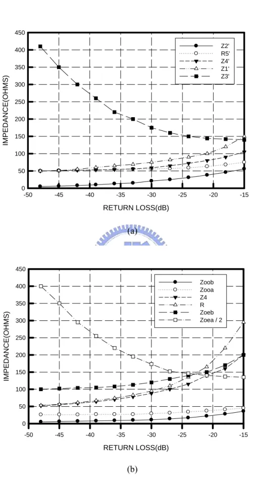
stripline (CPS) structures to implement the presented fifth-order balun network in next chapter. As the fourth-order Chebyshev filters having 5:1 bandwidth shown in
the Figure 4.4, the corresponding diagrams of the presented fifth-order balun between the design specifications and element values can be also established. The complete
RETURN LOSS(dB) -50 -45 -40 -35 -30 -25 -20 -15 IMP E DA NC E (OHMS ) 0 50 100 150 200 250 300 350 400 450 Z2' R5' Z4' Z1' Z3' (a) RETURN LOSS(dB) -50 -45 -40 -35 -30 -25 -20 -15 IM P E DA NC E (O HM S ) 0 50 100 150 200 250 300 350 400 450 Zoob Zooa Z4 R Zoeb Zoea / 2 (b)
Figure 4.4 The fourth-order chebyshev filters having 5:1 bandwidth. (a) Equivalent circuit parameters. (b) Coupled-line parameters.
The balun element values are all determined rapidly by checking the Figure 4.4. These two diagrams are established on 50Ω-system and the impedance transformation
ratio is equal to two. The impedance transformation is one of the important properties of balun. In next chapter, the presented balun is also mentioned that the design
procedures for different values of impedance transformation ratio.
4.2.2 Chebyshev Model Establishment
The mathematical model should be established before the network synthesis. In
general, Butterworth and Chebyshev polynomials are the common choices when we define the mathematical model for filter or balun design. In this section, Chebyshev
approximation is used to synthesize the following second-order and third-order baluns.
The exact broadband synthesis theory [29, 30] is a well design method to analyze the network responses using in the network consisting entirely of equal wavelength
lines, stubs and coupled lines. These are called commensurate lines. In next chapter, the complete design procedures of the novel fifth-order balun are presented.
Now, we have a short discussion about the Chebyshev model establishment of the second-order and third-order baluns by these following steps:
(1) An ideal balun is a three-port network which can separate the incident power into equal portions and 180-degree phase difference responses. For the two-port
condition of exact synthesis method, balun must be reduced to the equivalent two-port network. For example, the two 50Ω output impedances of balun can be viewed as a
series connection as a 100Ω load system.
(2) The Z-, Y-, and S-parameter representations are often used to characterize a
microwave network with arbitrary number of ports. However, in many practical microwave networks consist of several cascade connection forms. In this case, by
multiplying ABCD-matrix of the individual two-port sub-networks is a convenient way to easily derive the whole network representation. The basic definition for a
two-port network in terms of the total voltages and currents is given by
1 2 2 V =AV +BI (4.10.a) 1 2 2 I =CV +DI (4.10.b) or in matrix form as 1 2 1 2 V A B V I C D I = (4.11)
There are some useful transmission (ABCD-) parameters as shown in Table 4.1.
Z , o Z β Circuit Y l ABCD Parameters
1
0 1
Z
1 0
1
Y
0 0 cos sin sin cos l jZ l jY l l β β β β Table 4.1 The ABCD parameters of some useful two-port circuits.
(3) According to Richard’s transformation definition, the distributed network composed of commensurate length of transmission-lines and load resistance can be
treated as a lumped R-L-C network by using the complex frequency variable S for network analysis and synthesis. The complete exact synthesis method and Richard’s
transformation will be presented in chapter five.
The second-order model which is the minimum order of Marchand prototype
balun consists of only a series open-circuited and a shunt short-circuited stub. A series open-circuited stub can be regarded as a series capacitor in Richard’s domain and a
shunt short-circuited one is known as a shunt inductor. In the third-order model, a cascade transmission-line section is added behind the shunt short-circuited one.
From the Richard’s transformation theory, the corresponding transmission-line impedance transformations are introduced as follows [27].
0
1
- : C
Z
Series open circuited stub = (4.12)
0
- : L=Z
Shunt short circuited stub (4.13)
UE 0
: Z =Z
Cascade line (4.14) , where Z denotes the distributed transmission-line impedance in real frequency 0
domain; L and C are the corresponding lumped elements in complex plane (Richard’s) domain; Z is the corresponding impedance of unit element. The equivalent UE
circuits of second-order and third-order balun models are shown in Figure 4.5.
2 1 Z C = 3 Z =L C L 2 1 Z C = 3 Z =L C L 4 UE Z =Z (UE) Z ( )a ( )b
Figure 4.5 The equivalent circuits of Marchand baluns.
(4) Due to the unmatched impedance property of the equivalent two-port network, the conversions between S-parameter and ABCD-parameter should be
revised to the following equations.
02 01 02 01 11 02 01 02 01 AZ B CZ Z DZ S AZ B CZ Z DZ + − − = + + + (4.15) 01 02 21 02 01 02 01 2 Z Z S AZ B CZ Z DZ = + + + (4.16)
To simplify the analysis, the impedance transformation ratio 02 01
Z
Z is supposed to be 2 in this procedure. Finally, the complete mathematical representation of squared
magnitude of transmission coefficient parameter denoting as S212 can be derived by
several minute and complicated calculations in Richard’s domain. It is a polynomial of the complex frequency variable S. Table 4.2 shows some useful ABCD-parameters
in Richard’s domain.
Distubuted Circuit Lumped Circuit
1 1 0 1 SC 1 0 1 1 SL Z ABCD Parameters Z C L (UE) Z Z ( ) 2 ( ) 1 1 / 1 1 UE UE Z S S Z S −
The squared magnitude of transmission coefficient of the second-order balun network can be expressed as
2 21 2 2 4 2 2 2 2 2 4 1 (8 4 ) 4 1 8 S L C S LC L C S L C S = + − − + + (4.17)
, where L and C are lumped element values in Richard’s domain. They represent a quarter-wavelength shunt short-circuited and series open-circuited stub in real
frequency domain, respectively.
The third-order balun network can be defined as
2 21 ' 6 ' 4 ' 2 ' 6 4 2 0 4 2 1 1 (1 ) S F S F S F S F S S = + + + + − (4.18) ' 2 2 2 4 2 2 2 2 6 ' 2 2 2 2 4 2 3 2 2 3 2 4 2 4 ' 2 2 2 3 2 2 4 2 ' 2 0 2 2 2 (4 4 ) / ( 4 2 8 2 2 8 ) / (8 8 4 2 ) / (4 ) / 8 F Z L C Z L C L C F Z L C L Z C Z LC ZL C Z L C Z LC ZLC F Z LC ZL Z C Z L Z L Z F Z Z L C = − − ∆ = + + + + − − − ∆ = + − − − − ∆ = ∆ ∆ =
, where Z is the characteristic impedance of unit element in Richard’s domain. It represents a cascade quarter-wavelength transmission-line in real frequency domain.
∆
is the fractional bandwidth (FBW) of the balun; ' 6F , F , 4' F and 2' F are the 0'
coefficients of S to the power of six, four, square and zero, respectively. They are functions of Z, L and C.
(5) For the reason that the equivalent two-port network of balun can be viewed as a bandpass filter response, so we choose a high-pass Chebyshev prototype in complex
domain to model the desired design. The following two Chebyshev prototypes presented for second-order and third-order Marchand balun are shown in Figure 4.6
and 4.7. Specially, due to the special denominator form of ABCD-matrix of unit element, the Chebyshev polynomial is in need of some reasonable revisions. The
method of mathematical function establishment is dilated in chapter five.
This is a second-order high-pass Chebyshev polynomial form shown below.
2 21 4 2 2 4 2 2 2 4 1 1 4 4 1 ( C) 1 ( C C) N S S S S S S T S S ε ε = = + + + − + (4.19)
, where ε is expressed as ripple-level of Chebyshev response and its related response diagram is shown in Figure 4.6.