國立交通大學
顯示科技研究所
碩士論文
設計與製作結合有機電激發光元件及反射
式液晶之新型顯示器
Design and Fabrication a Hybrid Display of
Organic Electroluminescence Devices and
Reflective Liquid Crystal Displays
研究生:許傳偉
指導教授:謝漢萍 教授
設計與製作結合有機電激發光元件及反射
式液晶之新型顯示器
Design and Fabrication of a Hybrid Display of
Organic Electroluminescence Devices and
Reflective Liquid Crystal Displays
研 究 生: 許傳偉
Student: Chuan-Wei Hsu
指導教授: 謝漢萍 Advisor: Dr. Han-Ping D. Shieh
國立交通大學 電機學院
顯示科技研究所
碩士論文
A Thesis
Submitted to Display Institute
College of Electrical and Computer Engineering
National ChiaoTung University
in Partial Fulfillment of the Requirements
for the Degree of Master
In
Display Institude
June 2006
Hsinchu, Taiwan, Republic of China.
Design and Fabrication a Hybrid Display of
Organic Electroluminescence Devices and
Reflective Liquid Crystal Displays
Student: Chuan-Wei Hsu Advisor: Prof. Han-Ping D. Shieh
Display Institue
National Chiao Tung University
Abstract
A novel hybrid pixel structure of organic electroluminescence devices and RLCD is proposed and demonstrated. The hybrid pixel structure is designed to replace the backlight system of conventional transflective display with OLED as the emission component. Without the backlight module, the hybrid display is thinner and lighter than transflective LCDs. Moreover, the contrast ratio of the OLED in bright ambience can be improved by blocking undesired reflection with the modulation of LC layer. Prototypes of two proposed structures were fabricated and measured. From the experimental results, an enhancement of ambience contrast ratio of the emissive mode with gain factors of 14.35~19.04 and 6.14~7.10 for structure 1 and structure 2 were derived respectively, evidently demonstrated the readability of the hybrid display in all kinds of ambience intensity.
設計與製作結合有機電激發光元件及反射式液晶之新型顯示器
研究生:許傳偉 指導教授:謝漢萍 教授
國立交通大學顯示科技所
摘要
本篇論文中提出一結合有機電激發光元件及反射式液晶之新型顯示器,此結 合式畫素結構之設計目的為以有機發光二極體做為主動發光元件取代傳統透反 射式液晶顯示器中之背光系統。在除去背光模組後,本結合式顯示器會比透反射 式液晶顯示器得更加輕薄,此外,有機發光二極體在強環境光中操作之對比度問 題可以液晶層將不需要之反射光濾去而獲得改善。本論文所提出之兩種結構設計 皆製作出其原型並量測其效能,由實驗之結果可得,結構一與結構二之環境光對 比度之增益各可達 14.35~19.04 與 6.14~7.10 倍,此結果証實了結合式顯示器在 強度不同之環境光下之可讀性。致謝
首先要感謝指導教授謝漢萍老師兩年來在研究上、表達能力上及生活細節上 的細心指導,並提供良好的研究環境,讓我能同時學習液晶顯示器與有機發光二 極體之製作技術,並順利完成本論文。 在實驗室的日子裡,首先要感謝楊柏儒學長在各方面的指導與協助,還有黃 乙白、簡克偉、韋安琪、莊喬舜、楊柏儒、林泩宏、李企桓、鄭裕國、劉康宏、 鄭榮安及 Wallen 等實驗室的其他學長姐們提供他們保貴的經驗與意見,讓我受 益匪淺。同時感謝耀中、奕智、琬琳、宣儀、秀鳳、明倫、俞文等同學們在課業、 研究、生活上的幫助與分享,並陪伴我一起度過兩年碩士班的日子。我也感謝實 驗室的學弟妹與助理小姐讓實驗室充滿歡愉的氣氛。 此外,我要感謝工研院電光所的諸位合作同仁提供我寶貴的意見及實質的協 助,使我的研究更加的順利。 最後,對於我的家人與女友君頻,我要感謝你們多年來的栽培以及給我心理 上的支持與鼓勵,還有在生活上的細心照顧與關懷,使我能無後顧之憂的研究與 學習,並順利完成碩士學業。這份喜悅我將與每位關心我的人分享。Table of Contents
Abstract (Chinese) Abstract (English) Acknowledgments Table of Contents Figure Caption Chapter 1 Introduction ……….………11.1 Portable Display Technology………...1
1.2 Liquid Crystal Displays...………....1
1.2.1 Transmissive LCD………..1
1.2.2 Reflective LCD………...3
1.2.3 transflective LCD………...4
1.3 Organic Electroluminescence Displays ………..…...6
1.4 Motivation and Objective of this thesis ……….8
1.5 Organization of this thesis………..9
Chapter 2 Principle……….10
2.1 Overview...………10
2.2 Principle of Reflective Liquid Crystal Displays…..………..10
2.3 Operation Principle of EL devices……….…………14
2.3.1 Electroluminescence…………..……….……….14
2.3.2 Transparent and Top Emission EL structure………16
2.3.3 Transparent Cathode EL devices……….………..………...16
2.3.4 Passivation of EL Devices…………..……….……….18
2.4 Hybrid Display of R-LCD and Electroluminescence Device
2.4.1 The Structure of the Hybrid Display………....….……….22
2.4.2 The Operation Principle of the Hybrid Display……….23
Chapter 3 Simulated Results and Discussion 3.1 Overview….………...29
3.2 Fabrication Process………..29
3.3 Optical Performance Measurement System………..34
Chapter 4 Experimental Results and Discussions 4.1 Introduction….………...38
4.2 Results of Components……….…….…38
4.2.1 Results of Reflective LCD………38
4.2.2 Results of Reflective OLED……….42
4.3 Results of Hybrid Pixel Structure………46
4.3.1 The Contrast Ratio of the Hybrid Pixel Structure……….46
4.3.2 The Viewing Angle of the Hybrid Pixel Structure………....49
4.3.3 The Visual Appearance of the Hybrid Pixel Structure………..51
4.4 Discussion………...………52
4.5 Summary………57
Chapter 5 Conclusion and Future Work 5.1 Conclusion…....………...58
Figure Caption
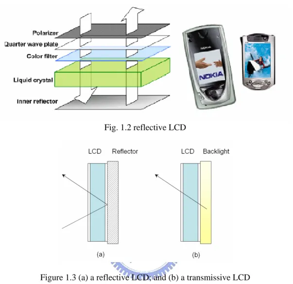
Fig. 1.1 Transmissive LCD………2
Fig. 1.2 reflective LCD………..4
Figure 1.3 (a) a reflective LCD; and (b) a transmissive LCD ………...4
Fig. 1.4 Transflective LCD………5
Fig. 1.5 Photos of an OLED display at the indoor and outdoor environments. ………7
Fig. 1.6 the ambient light is reflected by the EL device pixel ………...7
Fig. 2.1 (a) Schematic drawing of a direct view reflective LCD. (b) Schematic drawing of a projective reflective LCD. (c) The Azimuth angle of various components in the reflective LCD……...11
Fig. 2.2 The principle of electroluminescence (a) hole and electron Injection, (b) the charge transportation, and (c) recombination of hole and electron………15
Fig. 2.3 Structure of (a) bottom emission, (b) top emission, and (c) transparent devices………16
Fig. 2.4 the conventional encapsulation of OLEDs………..18
Fig. 2.5 Schematic of layer stack of a OLED with thin film encapsulation………….19
Fig. 2.6 The anti-reflective function of a circular polarizer can increase the CR of the EL device……….………....21
Fig. 2.7 Two different structural configurations of the hybrid display (a) structure 1 : EL device on R-LCD, and (b) Structure 2 : R-LCD on EL device………...23
Fig. 2.8 (a) the reflective mode of the hybrid display (b) the emissive mode of the hybrid display of structure 2………24 Fig. 2.9 (a) the reflective mode of the hybrid display and
(b) the emissive mode of the hybrid display of structure 1………26
Fig. 3.1 the flow chart of the new proposed fabrication process in which single-substrate LCD is employed……….33
Fig. 3.2 Schematic diagram of a conoscope……….34
Fig. 3.3 A directional receiver scanning the viewing cone of a display………...35
Fig. 3.4 Illustrations of the conoscope detector………....36
Fig. 3.5 the optical system of the conoscope………....36
Fig. 4.1 The R-V characteristic of the RLCDs……….39
Fig. 4.2 The iso-contrast graphs of (a) RLCD 1 and (b) RLCD 2………40
Fig. 4.3 The contrast ratio (a) in the horizontal and (b) in the vertical direction with respect to different viewing angle of RLCD 1 and (c) RLCD 2……….40
Fig. 4.4 The contrast ratio of the RLCD samples under different ambience intensity………..41
Fig. 4.6 the structure of the semi-transparent OLED………...42
Fig. 4.7 The transmittance of the semi-transparent OLED………..43
Fig. 4.8 (a) The front view and (b) the rear view of the emitting transparent OLED………..43
Fig. 4.9 The ambience contrast ratio of OLED………44
Fig. 4.10 The iso-contrast contour graph of the OLED………45
Fig. 4.11 The contrast ratio of the OLED measure under 600 Cd/m2 ambience luminance with respect to difference viewing angle………45
Fig. 4.12 The ambience contrast ratio of the hybrid pixel structures and the OLED………...47
(b) emissive mode of structure 1………..………50 Fig. 4.15 The viewing angle of the (a) reflective and
(b) emissive mode of structure 2………..50 Fig. 4.16 The photographs of the (a) reflective and (b) emissive mode of the two
hybrid pixel structures………..51 Fig. 4.17 Transflective LCDs using (a) single cell gap and (b) double cell gap……..52 Fig. 4.18 (a) Structure 1: hybrid display with OLED (top) and RLCD (bottom)
(b) Structure 2: hybrid display with RLCD(top) and OLED(bottom)………53 Fig. 4.19 Configurations of hybrid display proposed by (a) E. Lueder,
List of Tables
Table 2.1 Different transparent cathodes……….17 Table 4.1 The improvement in contrast ratio of the hybrid pixel structures…………47 Table 4.2 Comparison of different kinds of transflective display………53 Table 4.3 The comparison of different hybrid pixel structures of RLCD and OLED..56
Chapter 1
Introduction
1.1 Portable Display Technology
In the dawn of twenty-first century, a new era of 4C, which contains computer, communication, consumer electronics, car electronics, and 3G (the third generation mobile phone) is coming. It is the trend of future to transport greater amount of information through thinner and lighter interface. Thus, flat panel displays (FPD) with better performance which is more suitable for future life style are desired for people to fulfill the demand of these portable multimedia usages. In addition to the basic image quality, the required features of portable FPDs also include light weight, sunlight readability, and low power consumption. While the mainstream of FPD industry is recently held by LCDs (liquid crystal displays) [1], conventional transmissive LCDs which utilize backlight system as the light source do not seem to meet the requirements of portable displays due to its size and power consumption. Therefore, several display technologies have been developed in order to meet the requirements which are mentioned above. For example: transflective LCD, OLED displays are two of the most competitive display technologies in portable display applications.
1.2 Liquid Crystal Displays
1.2.1 Transmissive Liquid Crystal Display
applications. A transmissive LCD, which equipped with an illuminator called backlight is placed at the rear surface of the LCD panel, is used to exhibit information. The amount of light emitted from backlight is controlled by the liquid crystal panel to show images, as shown in Fig. 1.1. Although the transmissive LCD can provide higher contrast ratio and better color saturation by using backlight, the amount of transmitted light is relatively small. The backlight consumes 50% or more of the total power consumption of the display. Besides, the transmittances of polarizer and color filter are 50% and 30%, respectively. Therefore, a typical transmissive type LCD only has a light efficiency of about 7.4%. In order to get acceptable luminance, it can be solved by utilizing a brighter backlight, but the power consumption will be further increased. Moreover, the image of transmissive LCD will be washed-out under brighter environment. As a result, transmissive type LCD is not enough for portable applications.
LC panel Backlight system Analyzer Glass Color filter LC cell Pixel electrode Glass Polarizer Backlight Fig. 1.1 Transmissive LCD
1.2.2 Reflective Liquid Crystal Display
In order to overcome the issues of transmissive LCD, a reflective type LCD was proposed [2, 3], as shown in Fig. 1.2. The reflective type LCD is composed of a bottom reflector and a liquid crystal panel. Thus, the incident beam of light passes through the LC cell and is reflected by the bottom reflector. The beam of light undergoes a double passage through the LC layer twice before exiting the cell. The optical path difference between a transmissive LCD and a reflective LCD is shown in Fig. 1.3. It should be noted that the bottom reflector is the essential part in the reflective LCDs. On the whole, all transmissive LCDs can be employed for reflective LCDs. Due to the double passage of the beam of light, only one polarizer, the top polarizer, is needed to obtain polarization difference to switch between the bright state and the dark state. Because the image is exhibited by using reflector to reflect ambient light, the luminance of reflected light is close to that of the environment. Hence, the washout effect can be reduced substantially. Besides, the power consumption issue can be eliminated due to the removing of the backlight system. However, since the reflective type LCD uses the ambient light as the light source to present the images, the luminance of the reflected light thus highly depends on the ambient light, and always loses its readability in the dark environment. Furthermore, to control the optical properties of ambient light is difficult. As a result, the reflective LCD, which can not provide higher contrast ratio and color saturation under all environments, is limited for portable applications.
Fig. 1.2 reflective LCD
Figure 1.3 (a) a reflective LCD; and (b) a transmissive LCD
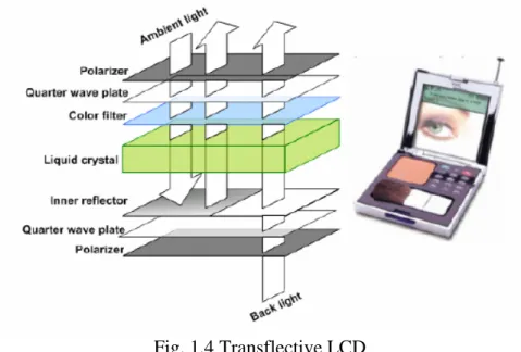
1.2.3 Transflective Liquid Crystal Display
In order to improve the issues of transmissive and reflective LCDs, a configuration
which realizes both the transmissive and reflective type display in a single liquid crystal device has been developed and named as transflective LCD [4, 5], as shown in Fig. 1.4.
Fig. 1.4 Transflective LCD
The liquid crystal displays using both the transmitted light and reflected light are generally referred to transflective LCDs, which can provide better image quality under any circumstance. A transflective LCD which comprises a transflector between liquid crystal cell and glass substrate is shown in Fig. 1.4. The transflector functions partially transmission and reflection. In the transmissive mode, backlight passes through transflector to display information. On the other hand, ambient light is reflected by transflector to realize images in the reflective mode.
1.3 Organic Electroluminescence Device
Electroluminescence (EL) is the generation of light by electrical excitation. The first report of EL from organic semiconductors was from Helfrich and Schneider in 1963 [6]. They demonstrated electroluminescence in thick (50μm to 1mm) crystals of anthracene. However, due to the high operating voltage (50~1000V) and the poor performance, these early devices were not practical. Breakthroughs of organic EL was made in 1980’s by Tang, VanSlyke, and Chen [7, 8]. They fabricated a dual-layer-device structure using molecular thin films (a few hundred angstroms) of 8-hydroxyquinoline aluminum (Alq3) as the emissive layer and aromatic diamine as the hole-transport layer. The organic layers were sandwiched between the anode ITO and the cathode Mg-Ag alloy. Its low operating voltage (<10V) and high luminance (up to 2000 cd/m2) immediately attracted researchers to continuously improve the device performance for practical applications.
In 1990, Burroughes and the co-workers at Cambridge University successfully demonstrated a polymer-based OLED using the conjugated polymer with low voltage operating [9, 10]. Again, this successful demonstration also triggered a lot of research on polymer light emitting diodes (PLED).
The operating voltage, brightness, and the color performance of current OLEDs are eligible for many display applications, either as backlight sources or directly as emitter in emissive displays. Compared with the currently dominant LCD technology, FPDs made of OLEDs have the inherent advantages of emissive displays, its wide viewing angle. In addition, due to the flexible nature of the OLED materials, flexible flat panel displays for portable electronics is made possible [11, 12, 13]. The
The contrast ratio (CR) of OLED display exhibited by Samsung in 2005 can reach 5000:1 in dark ambience, as the photo shown in Fig 1.5, while the contrast ratio of LCD is only 1000:1. This difference is due to the display principles. But EL displays have its own drawbacks. As a result of the multilayer structure of EL devices, these layers, especially the metal cathode, are high reflectance surfaces, thus, while operating outdoors or under bright ambience, the inactivated pixel will reflect the ambient light which makes the CR lower. Besides, the photoluminescence is induced because of the absorption of the UV in the sunlight. The phenomenon will induce a serious decrement of the contrast ratio of the EL displays and make the image illegible. This is called as wash-out phenomenon of EL devices, as shown in Figs. 1.5 and 1.6.
Fig. 1.5 Photos of an OLED display at the indoor and outdoor environments.
1.4 Motivation and Objective of this Thesis
Transflective LCDs can be operated both indoors and outdoors. When operating indoors, a transflective LCD works as conventional transmissive LCD, the backlight system serves as the light source. While for outdoors operation, it is switched to the reflective mode. Backlight is turned off and the total power consumption is fairly low. But comparing with a reflective LCD where no backlight is used, the size and low aperture ratio of transflective LCDs are two concerns.
On the other hand, EL devices such as OLED or PLED are self-emitting devices which can operate without the backlight system. Thus, the thickness is comparatively thin to transflective LCDs. But, as it was mentioned previously, the contrast ratio of OLED display for outdoor operation is poor, and the washout phenomenon makes the image illegible.
Since both displays are superior to the other in different ambient light, we present a hybrid display which combines a reflective LCD and an EL device in a single structure by stacking two devices together. The hybrid display can be switched between two modes : the reflective mode and the Emissive mode. The reflective LCD can compensate the poor contrast ratio of EL device in bright ambient light. While the EL device replaced the backlight system of transflective LCD, which make the total thickness and weight reduced from the original transflective LCD.
In such a stacking configuration, the pixel area of the hybrid display is not divided into the transmission region and the reflective region as transflective LCDs. Thus, the aperture ratio will not be decreased and the light efficiency is higher than the conventional transflective LCDs.
1.5 Organization of this thesis
The thesis is organized as following: the principles and the features of the proposed hybrid display will be presented in Chapter 2. The mode of operation will also be discussed. In Chapter 3, the fabrication process to realize our hybrid display of R-LCD and EL device is summarized. The measurement equipments will be illustrated. In Chapter 4, the fabricated hybrid display of R-LCD and EL device will be demonstrated. Further, the measurement results including optical and electrical performances will be evaluated. The summary of the dissertation and the future works are given in Chapter 5.
Chapter 2
Principle
2.1 Overview
An overview of the basic display principle of reflective LCD and EL display will be given in this chapter respectively. Then, two different structures of the proposed hybrid display and their operation principle will be shown.
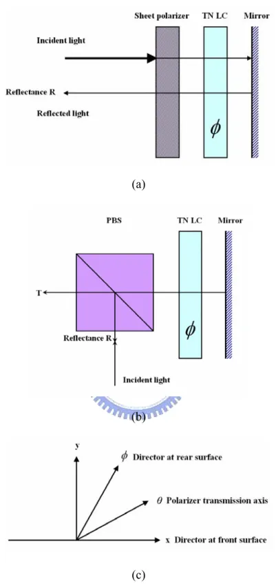
2.2 Principle of Liquid Crystal Displays 2.2.1 Reflective LCD
Liquid crystals can be employed for display applications after combining with the backlight. Transmissive mode LCDs require two polarizers to control the intensity modulation at each pixel. The input polarizer prepares a linear polarization state before entering the LC layer. The analyzer is employed to achieve the polarization interference to produce the black or the dark state. If the backlight is replaced with a mirror and the light is illuminated from the front, only one polarizer is needed since the light passes through the LC layer twice. For direct-view applications, the light is provided by the ambient light. Reflective LCDs can also be employed for projection displays. Next, the property of general twist nematic (TN) LCD with a back mirror which is employed in our design will be introduced. Referring to Fig. 2.1a, a reflective display that employs a TN-LC of STN-LC sandwiched between a sheet polarizer and a mirror is set up. This configuration is used for direct view reflective displays [16, 17, 18]. For projective applications, the sheet polarizer is replaced with a polarizing beam splitter (PBS), as shown in Fig. 2.1b.
(a)
(b)
(c)
Fig. 2.1 (a) Schematic drawing of a direct view reflective LCD. (b) Schematic drawing of a projective reflective LCD. (c) The Azimuth angle of various components in the reflective LCD. The x axis is chosen to be parallel to the director at the input surface. φ is the total twist angle of the LC layer, θ is the angle of the transmission axis of the polarizer.
First, the reflection and transmission properties of the reflective LCD in the off state at normal incidence are considered. According to Fig. 2.1b, the incident and reflected polarization states, as determined by the orientation angles of the polarizer reflection axis, are given by
⎟⎟ ⎠ ⎞ ⎜⎜ ⎝ ⎛ = ⎟⎟ ⎠ ⎞ ⎜⎜ ⎝ ⎛ θ θ sin cos y x V V , ⎟⎟ (2- 1) ⎠ ⎞ ⎜⎜ ⎝ ⎛ = ⎟⎟ ⎠ ⎞ ⎜⎜ ⎝ ⎛ θ θ sin cos ' ' y x V V
where θ is the angle of the plane of polarization of the incident and reflected beam. Assuming an incident beam of polarized light, the intensity of reflectivity of the LCD shown in Fig. 2.1 is given by, according to the Jones matrix method
2 ~ ' 2 1 MV M V R= • (2- 2) ⎟⎟ ⎟ ⎟ ⎠ ⎞ ⎜⎜ ⎜ ⎜ ⎝ ⎛ Γ + − Γ − = X X i X X X X X X X i X M 2 sin cos sin sin 2 sin cos φ φ (2- 3)
where M is the Jones matrix of the LC cell, the tilde ~ indicates a transpose operation, and V and V’ are the incident and reflected Jones vectors, respectively. Using Eq. (2- 1) for M, and Eq. (2- 3) , after a few steps of matrix multiplication, the reflectivity is obtained that 2 2 1 iB A R= + 2 2 2 2 2 2 2 sin 4 sin cos X X X X X A= +φ −Γ (2- 4) ⎥⎦ ⎤ ⎢⎣ ⎡ + Γ = X X X X X
B sin cos2θcos sin2θφsin
where θ is the angle between the angle of the reflection axis of the PBS measured from the local director at the input surface, φ is the total twist angle of the LC cell, and X is given by
The reflectivity can also be written as 2 2 2 2 2 2 2 2 sin 4 sin cos 2 1 ⎥ ⎦ ⎤ ⎢ ⎣ ⎡ + −Γ = X X X X X R φ 2 sin 2 sin cos 2 cos sin 2 1 ⎭ ⎬ ⎫ ⎩ ⎨ ⎧ ⎥⎦ ⎤ ⎢⎣ ⎡ + Γ + X X X X X θ θφ (2- 6)
By using the Mauguin parameter u such that
2 1 u X =φ + with φλ π φ nd u= Γ = Δ 2 (2- 7) The reflectivity can be written as
2 2 2 2 2 2 2 2 2 2 1 sin 2 sin 1 sin cos 2 cos 2 sin 1 1 cos 2 1 ⎭ ⎬ ⎫ ⎩ ⎨ ⎧ + + + + ⎭ ⎬ ⎫ ⎩ ⎨ ⎧ + − + = u X u X X u X u u X R θ θ (2- 8)
The transmission is given by
T=1-R (2- 9) In the case when a sheet polarizer is used, as shown in Fig. 2.1a, Eq. (2- 8) is the reflectivity of the reflective display system, where θ is the angle of the transmission axis of the polarizer measured from the local director at the input surface.
By examining Eq. (2- 8) for the reflectivity, it is found that for a given TN-LC or STN-LC cell with a twist angle φ and a Mauguin parameter u, the reflectivity R is a periodic function of the angle θ. By differentiating Eq.(2- 8) with respect to the angle θ, the following maximum and minimum reflectivity is obtained:
2 2 2 2 2 min 1 sin 1 cos 2 1 ⎭ ⎬ ⎫ ⎩ ⎨ ⎧ + − + = X u u X R , when X u tan 1 2 tan θmin =− + 2 (2- 10) And 2 1 max = R when 2 max 1 tan 2 tan u X + = θ (2- 11)
0 min = R when 1 1 tan 22 − + ± = u u X (2- 12) In summary, Rmin is always possible provided the polarizer orientation angle θ
satisfies the condition Eq.(2- 11). On the other hand, full reflection (Rmax=0.5) is
possible provided that the Mauguin parameter satisfies the condition (2- 12).In other words, a normally black TN-RLCD which can switch reflectivity from 0 to 0.5 is possible through the designed setup.
2.3 Operation Principle of EL Devices 2.3.1 Electroluminescence
The emitting principle of electroluminescence can be explained in three steps. As show in Fig. 2.2, when a positive voltage is applied across the electrodes, the holes and electrons will be injected into the highest occupied molecular orbital (HOMO) of the hole transporting layer (HTL) and the lowest unoccupied molecular orbital (LUMO) of the electron transporting layer (ETL) respectively. In the second step, electric charge is driven by the electric field and transported to the interface of the HTL and the ETL. Due to the difference in energy levels at the interface, there will be charge accumulation at the interface. After that, when the holes and electrons recombine in the emissive material, excitons are generated. The excited state of the excitons is an unstable state. So, the energy will be released in the form of light and heat and return to the ground state. Thus, the electroluminescence is a current-driven process.
(a)
(b)
(c)
Fig. 2.2 The principle of electroluminescence (a) hole and electron Injection, (b) the charge transportation, and (c) recombination of hole and electron.
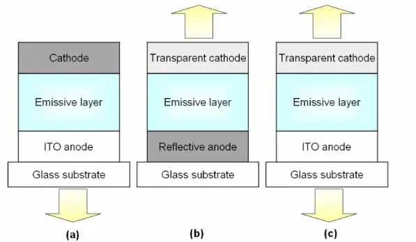
2.3.2 Transparent and Top Emission EL Structure
Conventional EL devices emit light from the bottom substrate, this is so called the bottom emission. While the top emission referred to the emitted light does not pass through the bottom substrate but goes in the other direction. As shown in Fig. 2.3b, if the anode on the substrate has high reflectance and the cathode is transparent, the emitted light will pass through the cathode. If the electrodes are conventional ITO anode and transparent cathode, both sides of the device emit light. This is so called the transparent devices [19], as shown in Fig. 2.3c.
Fig. 2.3 Structure of (a) bottom emission, (b) top emission, and (c) transparent devices
2.3.3 Transparent Cathode and Passivation of EL Devices
Among the transparent and top emission device structures, the most important part is the transparent cathode. In order to let the light pass through the cathode, the most direct way is to make the cathode of a bottom emission device extremely thin. So there will not be any work function issue. The most suitable metals for the injection of the electrons into the organic layers are Al, Ag, Mg, and Ca. Single and
conductivities and transmittance. All metal layers were deposited by the vacuum thermal evaporation technique which is harmless to the emissive layer of the EL devices. However, when the cathode is extremely thin, the metal tends to be oxidized easily. Thus, ITO is often deposited onto the cathode as the assistant electrode to increase the conductivity of the cathode. Nevertheless, sputtering ITO onto organic layer without damaging the device is not easy and needs techniques to overcome. Different kinds of transparent electrodes and their corresponding transmittance are shown in table 2.1.
In our proposed structures, two kinds of EL devices are used. One is bottom emission EL device, the other is transparent EL device. For the cathode of the transparent device, in order to obtain a high transmittance without any damaging process, the transparent cathode adopted is Ca/Ag cathode structure [20, 21].
Table 2.1 Different transparent cathodes [22]
Cathode structure Tmax Device struture
Mg:Ag(10nm) /ITO (40nm) 70% transparent
CuPc/ITO 85% transparent
CuPc/Li (1nm) /ITO -- transparent
BCP/Li (0.5~1nm) /ITO 90% transparent
Ca (10nm)/ITO (50nm) 80% transparent
LiF (0.3nm) / Al (0.6nm) /Ag (20nm) /Alq3 -- top emission
LiF (0.5nm) / Al (3nm) /Al:SiO (30nm) -- top emission Ca (12nm) /Mg (12nm) /ZnSe 78% top emission
Ca (20nm) /Ag (15nm) -- top emission
Ca (10nm) / Ag (10nm) 80% top emission
2.3.4 Passivation of EL Devices
In order to inject holes and electrons into the emission layer, the most direct method is to lower the injection energy barrier. Because most the energy level of the emission materials’ LUMO are about 2.5-3.5 eV, and the energy level of HOMO is 5-6 eV. Thus, the material of cathode must be metals with low work function corresponding to the anode with high work function. While the low work function means the activity of the cathode material is high, the cathode will be oxidized easily. The oxidation of cathode will result in the failure of the EL device. Thus, the encapsulation of the EL device which isolates the device from the intrusion of water vapor and oxygen is very essential to the EL device.
Conventional EL device is encapsulated with a glass or metal lid, as shown in Fig. 2.4. The EL device is encapsulated by sealing the glass or metal lid on the EL device with glue in an inert atmosphere, such as nitrogen or argon. The method makes the thickness of the device increased. Besides, metal or glass lids will require a relative wide glue edge which makes it unsuitable for small size OLED displays.
Fig. 2.4 the conventional encapsulation of OLEDs
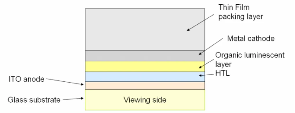
By replacing these coverings with a thin film encapsulation (TFE) layer [23, 24], the advantage of EL display in thickness is restored. Another benefit of thin film packaging is that smaller displays are enabled without the sealing border. Furthermore,
If the TFE is transparent, it can also be used for top emitting displays.
In metal or glass packaging, a getter such as calcium oxide or barium oxide is needed to absorb gas produced by the display sealing processing. The getter absorbs also residual water that is present after sealing or desorbed from the glass. Usually, this getter is situated on top of the cathode since placing the getter on the side would increase the sealing border width of the device. For thin film packaging, no getter is required, since it is in direct contact with the active layers of the device, no residual water is present. On the other hand, there are a few stringent demands, which the thin film encapsulation has to fulfill. First, it has to be a very good diffusion barrier to water and oxygen penetration. Secondly, it has to be free of pinholes. Furthermore, the encapsulation layer must be made as mechanically robust as glass or metal lids. This could be done with extra protection layers on top of the thin film packaging layer. Moreover, the TFE must be compatible with the processing of the active layers beneath. It is quite clear that the encapsulation layer has to be deposited after the organic deposition and cathode deposition. This procedure limits the processing possibilities, since the organics cannot withstand high process temperature and also require an inert processing environment. A schematic of TFE of EL device is shown in Fig. 2.5.
TEF is essential to the proposed hybrid display because the spacing between the two devices, the LCD and the EL device, must be as small as possible to eliminate the parallax effect resulting from the difference in depth of view. Furthermore, the hybrid display is possible for flexible and active matrix driven application as long as the TFE can provide a flexible encapsulation which enables the via connecting from the TFT backplane. While conventional glass lid is non-flexible and too thick for via to connect the cell to the backplane AM driving circuit. But to avoid the complexity of multilayer TFE and to facilitate the whole process, glass lid encapsulation of EL device will be adopted in our prototype demonstration.
2.3.5 Contrast Ratio of EL Display
After the structural consideration, image quality improvement for the hybrid display will be introduced. Contrast ratio (CR), defined as the ratio of the luminance of the display in bright state to that in the dark state, is an important feature of a display and also an index of the readability of the image. A good CR can compensate the shortage of brightness, while under poor CR, the appearing image quality will be poor even with sufficient brightness. As it is mentioned in chapter 1, the CR of EL devices under bright ambient light suffers from the reflection of each layer of itself. The contrast ratio with ambience reflection is defined as Eq. (2-13).
amb off amb on L R L L R L CR × + × + = (2- 13)
Where Lon is the luminance of the activated pixel, Loff is the luminance of the
inactivated pixel, R is the reflectance of the interface, and Lamb is the luminance of the
ambient light. Thus, a higher contrast ratio of EL can be obtained with a brighter bright state and a darker dark state.
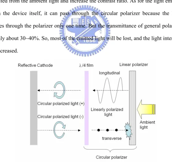
CR. Hence, the image will be washed-out while the CR is severely decreased. This problem can be solved by adding a polarizer which is often used in LCDs, as shown in Fig. 2.6. Taking circular polarizers for example, the circular polarizer is comprised of a linear polarizer and a quarter wave retarder. the angle between the axis of the retarder and the polarizer is 45°. After the incident light passes through the circular polarizer, the beam of light is turned into a circular polarized light. After being reflected by the cathode, the beam of light passes through the retarder for the second time. The circular polarized light returned to a linear polarized light and the polarization is 90° different from the original incident light. Thus, the reflected light can not pass through the linear polarizer. This method can reduce the reflectance resulted from the ambient light and increase the contrast ratio. As for the light emitted from the device itself, it can pass through the circular polarizer because the light passes through the polarizer only one time. But the transmittance of general polarizer is only about 30~40%. So, most of the emitted light will be lost, and the light intensity is decreased.
Fig. 2.6 The anti-reflective function of a circular polarizer can increase the CR of the EL device.
The mechanism of the CR improvement of hybrid display is similar to that of the circular polarizer. While the TN LC plays the role of the quarter wave plate. But unlike the circular polarizer, the hybrid display provides not only the antireflection function but also the reflective mode operation which utilize ambient light as the light source.
2.4 Hybrid Display of R-LCD and Electroluminescence Device 2.4.1 The Structure of the Hybrid Display
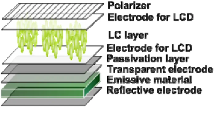
The proposed hybrid display stacks EL device and R-LCD with two types of configurations. The first structure is a stack of an EL device over a RLCD, as shown in Fig. 2.7 (a). The whole structure comprises the reflective electrode, the LC layer, the top electrode of LCD, the passivation layer, the transparent anode of the EL device, the emissive material of the EL device, the ITO anode of the EL device, the top glass, and the polarizer sequentially from the bottom to top. It should be noted that the EL device used for the first structure (EL device on RLCD) is a transparent type structure where a highly transparent metal serves as the cathode. The R-LCD in the hybrid display can be any mode of nematic liquid crystal displays, such as TN, STN, VA mode LCD or cholesteric liquid crystal display. The second structure is the reverse of the first structure. the R-LCD is stacked on the EL device. As the Fig. 2.7b shows, the EL device for structure 2 is a top emission structure of which the anode cathode is transparent.
(b)
Fig. 2.7 Two different structural configurations of the hybrid display (a) structure 1 : EL device on R-LCD and (b) Structure 2 : R-LCD on EL device
2.4.2 The Operation of the Hybrid Display
In the following section, the operation principle of both structures will be introduced respectively. For the explanation, a NB-TN LCD will be applied as the R-LCD part.
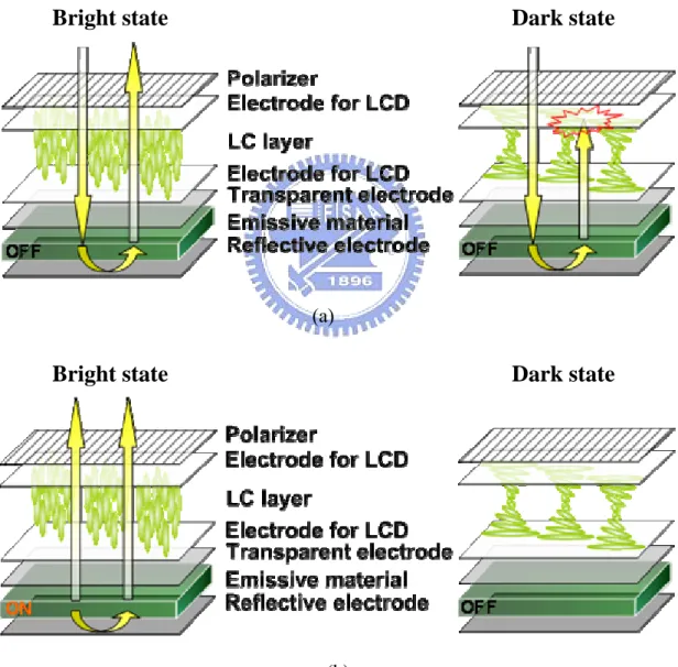
For the operation of the second structure, it can be operated in two modes : the reflective mode and the emissive mode. For the reflective mode operation, the EL device is turned off. Thus, the whole device is operated as a R-LCD. To obtain the bright state, a voltage is applied to the TN-LC layer and an electric field is induced so the LC molecules are aligned homeotropically perpendicular to the plate. Therefore, the incident ambient light, for example at normal incidence, will pass through the polarizer and be linearly polarized. Then, the polarized light will pass through the LC layer and reach the bottom reflector. After being reflected by the bottom reflector, the beam of light will retrace and pass through the polarizer again and the bright state is attained. To obtain the dark state, the voltage between electrodes is removed and the electric field turns to zero. The 45° TN-LC can be taken as a λ/4 plate. Thus, the linearly polarized incident light will undergo a phase retardation and become circular
polarized. After being reflected by the reflector, the beam of light passes through the LC layer for the second time. The circular polarized light returns to a linear polarized light and is 90°different from the original incident light. The principle is similar to that of the circular polarizer method which is mentioned in section 2.3.5. Thus, the reflected light will be blocked by the linear polarizer. The schematic of the operation is shown in Fig. 2.8 (a). The reflective mode is activated when the ambient light is sufficient to reduce the power consumption.
Dark state
Bright state
(a)
Bright state
Dark state
(b)
emissive mode. Comparing with the transmissive mode of transflective LCDs in which the whole backlight system is turned on, the emissive mode of the hybrid display selectively activate those pixels which need to be turned on. For the emissive mode operation of the structure 2, the TN-LCD still needs to switch on and off respectively for bright and dark state to reduce the undesired reflection of ambient light. While the EL device remains its ordinary operation in the emissive mode. So, in the bright state, the EL device is driven by the current and emits light. Generally, the light emitted from the EL device is isotropic. Thus, the upper half of the light will directly go up and pass through the LC layer and the polarizer. The lower half of the light will go down to the reflector, and go up after the reflection. Furthermore, both the EL device and the R-LCD are switched off in the dark state. Therefore, there will be neither emissive light from the EL device nor reflected ambient light. This schematic of the emissive mode operation is shown in Fig. 2.8b.
Because of the R-LCD/EL device configuration of structure 2, the light emitted from the EL device is partially absorbed by the LC layer and the polarizer. The transmitted proportion of the light emitted from the EL device is less than 50% in the first structure. Furthermore, the features of EL device such as wide viewing angle or fast switching will be eliminated due to the coverage of LC layer. In order to retain all the superior features of EL displays, we proposed a modified structure which reverses the structure and make EL device on the top of LC layer.
The operation principle of the structure 1, the EL device over R-LCD one, is shown in Fig. 2.9. Unlike structure 2, structure 1 adopts EL device as the main component. Thus, the operation mode is different from that of structure 1. When the ambient light of the surrounding is dim, the emissive mode can be activated. EL device actively emits light. The light can directly reach viewer’s eyes without being blocked by the LC layer. Thus, the emissive mode operation of structure 1 is much
like conventional OLED displays. While the ambient light is bright enough, it can be switched to the reflective mode. Owing to the dual mode operation of structure 1, it enables the readability under any condition.
Dark state
Bright state
(a)
Bright state
Dark state
(b)
Fig. 2.9 (a) the reflective mode of the hybrid display and (b) the emissive mode of the hybrid display of structure 1.
To demonstrate the operation of the hybrid display in detail, the emissive mode will be first introduced. In the emissive mode operation, the bright state is obtained by turning on the EL device and switching the R-LCD part to the bright state. The upper half of the light emitted from the EL device will directly be output. While the lower half of the light emitted from the EL device will be reflected by the R-LCD and out put. There will be a loss of light which is about 50% resulted from the absorption of the linear polarizer on the top of the structure. If in-cell polarizer is employed, only half of the light emitted from the EL device will be absorbed. Then, the loss can be reduced to 25%. But in our prototype demonstration, the polarizer is put on the top of the structure to facilitate the whole process. But comparing with the transmissive mode of the first structure of which the loss of light is 50%, structure 1 has better light efficiency.
As for the reflective mode of structure 1, the whole device can be regarded as a R-LCD covered with a semi-transparent film as the EL device is inactivated. Thus, the incident ambient light will be partially absorbed by the EL device. The transmittance of the EL device depends on the emission layer and the cathode, especially the cathode. The reflected light undergoes a double passage through the EL device which means the intensity of reflected light is attenuated twice by the EL device. So, the cathode of the EL device must be made thin enough otherwise the reflected intensity will be very weak.
Tthe configuration decides the two structures’ performance of each mode. The component on the top of the other can retain its original feature, while the performance of the lower component will be debased due to the top shielding of the upper component. Structure 2 is more favorable for reflective mode operation while structure 1 is more favorable for emissive mode operation. This hypothesis will be verified in chapter 4.
2.5 Summary
The basic operation principle of R-LCD and EL device are introduced in this chapter. The thickness and transmittance of the EL device’s electrodes decide the light emitting behavior of the devices. Two structures of the hybrid display have been proposed. The first structure of the hybrid display is comprised of a transparent type EL device and a R-LCD. The second is comprised of a R-LCD over a top emission type EL device. Both structures are designed for dual mode operation, reflective mode and emissive mode, under bright and dim ambience. The optical performance of each structure is more favorable of certain mode due to the difference in structural configuration. The performance of the hybrid display will be measured and shown in chapter 4.
Chapter 3
Fabrication and Measurement
3.1 Overview
A preliminary structure will be used to demonstrate the features of the hybrid display of R-LCD and EL device. The embodiment including several fabrication processes will be shown in the following sections, and all the fabrication process, technologies and instruments which are available to develop such a preliminary structure will be introduced in this chapter. First, the fabrication process includes wet etching, thermal evaporation, spin coating, exposure, development, sputtering, and liquid crystal injection. Besides, the features and performance of the fabricated structure and each component, such as the luminance, contrast ratio and contrast ratio enhancement were measured by Conoscope. The major features of the Conoscope will be illustrated in this chapter.
3.2 Fabrication Process
The fabrication of the hybrid display is basically the integration of the R-LCD and EL device processes. As it was mentioned, the best integration of R-LCD and EL device is done through thin film encapsulation which provides a robust barrier to prevent the intrusion from the water vapor and oxygen and remains the thin structure. However, in our prototype demonstration, conventional glass lid will be employed as the encapsulation of EL device to avoid the multilayer TFE process and simplify the fabrication process. Moreover, EL devices comprehend organic light emitting diodes and polymer light emitting diodes. The prototype of our hybrid display will adopt OLED as the EL device part.
As it was mentioned in chapter 2 that there are two different structures of the hybrid display, each of them is the reverse of one another. For our prototype demonstration, both of the structures are fabricated to compare their optical performance. Due to the similarity of fabrication process, only the fabrication of the structure 1 (EL device on R-LCD) will be given in the following section.
The detail steps to produce the prototype are listed below.
(a) The R-LCD part
(1) Alignment layer process: the material of the alignment layer is polyimide (PI). To form the alignment layer, PI is spin coated onto the first glass substrate. Then, a hard baking is applied to solidify the PI film. Next, the PI film is rubbed with a roller to form tiny grooves which LC molecules align with. It should be noticed that any high temperature process might cause the degradation of the OLED after the PI rubbing process. Thus, the RLC is proceeded first so that the OLED will not be damaged during the alignment layer process.
(2) Providing the second substrate: R-LCD requires a reflector. In our designed structure, the reflector is the reflective electrode on the second substrate. Thus, the second substrate is coated with aluminum and then patterned through wet etching. Then, photo spacer is formed to provide the LC cell a homogeneous cell gap. After that, the alignment layer process is proceeded on the reflective electrode.
(3) Cell assembly and LC injection: next, the LC cell is assembled by sealing the prepared second substrate to the first substrate with UV glue.
(b) The OLED part
(1) Glass preparation: For the display application, the glass is widely used as substrate. In the fabrication, the sodaline double-side polished glass with 0.7mm thick was chosen.
(2) ITO coating: The anode for transparent type OLED is made with ITO which is highly transparent for visible spectrum. The ITO is sputter on to the glass substrate and then patterned as the anode of the OLED.
(3) Hole transport layer depositing: the material of HTL, NPB, is thermal evaporated ted on the first substrate.
(4) Emission layer depositing: the emissive material of OLED in the prototype is Alq3. The emissive material is thermal evaporated onto the HTL
by a thermal evaporator.
(5) Thermal evaporation of cathode: the cathode of the transparent type OLED must be thin enough to let the light pass through. A double layer structure of calcium and silver is coated by thermal evaporation. The thickness of calcium and silver are both 50 nm.
(5) Encapsulation of OLED: the encapsulation of the OLED part of the hybrid display is made with the RLCD cell as the glass lid and sealed by UV glue.
(c) Characterization : after the fabrication the optical performance will be measured.
Another fabrication process which employs the single-substrate LCD process [25] is developed. The fabrication process of the prototype is a sequential process which R-LCD is encapsulated on the OLED. The temperature resistance of OLED is weak. Thus, the sequential process may cause damage to the OLED during the high
temperature alignment layer process. While the fabrication of the single-substrate LCD can be entirely independent from the process of the EL device, and the two devices are combined thereafter. It ensures that the EL device will not be damaged during the R-LCD process.
The fabrication of the hybrid display which uses single-substrate LCD is proceeded by separating the process into
(a) The EL part :
each layer of the EL device is sequentially coated onto the substrate. Thereafter, the passivation of the EL device is proceeded with TFE. The objective of this second fabrication process is to isolate EL device process from LCD process and also reduce the thickness of the whole device. Hence, glass or metal lid encapsulation is not suitable here.
(b) The LCD part :
single-substrate LCD is fabricated by confining the LC between a substrate and a protection layer. Because the alignment layer is only provided on the side of the substrate, the corresponding LC mode will be single-sided alignment mode, such as in-plane switching (IPS) mode. The single-substrate LCD process is an ideal fabrication process but is not performed in our present work. Each step can proceed in several ways. Thus, only the sequence is given but not the practical methods. The steps of the single-substrate LCD process are listed below:
(1) The second substrate is provided.
(4) The alignment layer is formed on the electrode. (5) The liquid crystal is dripped on the alignment layer. (6) The protection layer is formed on the LC layer.
(c) The combination :
after the two components are fabricated respectively, the LCD and the EL device are combined. The reflector for the R-LCD is formed at last.
The flow chart of the new fabrication process is shown in fig. 3.1.
Fig. 3.1 the flow chart of the new proposed fabrication process in which single-substrate LCD is employed.
3.3 Measurement System
components of the hybrid display, the R-LCD and OLED, are also fabricated. Thus, the inspection will be performed to measure each components and the hybrid display and demonstrate the image quality improvement of the hybrid display. Therefore, the optical performance measurement system, the conoscope will be demonstrated.
3.3.1 Optical performance measurement systems
After the preliminary fabrication of the hybrid display of R-LCD and EL device, we used a measurement instrument, conoscope, to measure the luminance, contrast ratio, and reflectance.
3.3.1.1 ConoScope
(a) Introduction:
Fig. 3.2 Schematic diagram of a conoscope
The ConoScope can be used for visual performance evaluation, such as luminance, contrast ratio, color shift, gray scale and many characteristics, as shown in
typical scanning device called "gonioscopic system" would scan the half cone above the display to detect the variations of luminance and color for each specific direction, as it can be seen in the upper right part of Fig. 3.3. Plotting each azimuthal angle on a circle was the radius from the center additionally indicates the polar angle results in the polar coordinate system, as shown in the left upper part of Fig. 3.3. Using such a polar plot to mark for each direction luminance and color will result (in the case of color) a colored figure, shown in the lower part of Fig. 3.3
Fig. 3.3 A directional receiver scanning the viewing cone of a display
An arrangement of several lenses (here represented by one single lens) modifies the light propagation directions in a way that all beams emerging from the sample in the same direction will meet in one spot in the focal plane. The Conoscope lens projects all parallel beams on one spot in the focal plane. The resulting figure is called the "conoscopic figure". This means, that each spot on the focal plane or within the "conoscopic figure" corresponds to one specific direction of the viewing cone. The conoscopic figure directly shows color and luminance as they would have been
plotted in a polar coordinate system as described under figure 3.4. Sample Measurement spot Conoscopic lens All parallel rays
forming one spot in the focal plane The conoscopic figure as a result of the interfering light beams for all propagations Sample Measurement spot Conoscopic lens All parallel rays
forming one spot in the focal plane The conoscopic figure as a result of the interfering light beams for all propagations
Fig. 3.4 Illustrations of the conoscope detector.
The apparatus is based on the well known conoscopic method where a cone of elementary collimated light beams C, transmitted by the sample S (S is located in the front focal plane of the conoscopic lens L1) and originating from the measuring spot is collected simultaneously over a large solid angle by the lens L1 as sketched in Fig 3.5.
Fig. 3.5 the optical system of the conoscope where
C: Cone of converging elementary parallel beams illuminating the transmissive sample S;
A2: variable aperture,
L2: relay lens for projection of IF1 to detector array in the plane of IF2
A pattern IF1 is generated in the rear focal plane F'1 of the lens L1 with the intensity of each area element corresponding to the intensity of one elementary parallel beam with a specific direction of light propagation.
The light propagating parallel to the optical axis of the conoscopic receiver forms the center of that circular pattern IF1 and beams with constant angle of inclination q form concentric circles around the center with the radius of the circles being proportional to the inclination q.
In the pattern IF1 the directional intensity distribution of the cone of elementary parallel light beams C is projected into a two-dimensional intensity distribution with each location in the pattern corresponding to one direction of light propagation (q, f).
A second optical system L2 optionally projects the pattern IF1 on a two-dimensional detector array (e.g. electronic camera) for evaluation of the spatial intensity distribution which corresponds to the directional intensity distribution of the light emerging from the measuring spot on the sample.
Chapter 4
Experimental Results and Discussions
4.1 Introduction
To demonstrate the optical performance of the hybrid pixel structure, the two types of hybrid pixel proposed in chapter 2 were fabricated in this thesis work. Standard reflective LC pixel structure and OLED component were also made to compare with the proposed hybrid pixel. For the R-LCD, the V-R characteristic, viewing angle, and the ambient contrast ratio were measured. The optical performance including transmittance, I-V-L characteristic, and contrast ratio of the OLED were derived through the measurements. Also, the emissive and reflective mode of the hybrid pixel operated in different ambience condition are examined and measured. At the end of the chapter, the experimental results will be compared with the prior arts.
4.2 Results of Components 4.2.1 Results of Reflective LCD
Two types of RLCD were fabricated for each hybrid pixel structure. For the structure 1, a RLCD equipped with diffusive micro slant reflector (DMSR) [26] was fabricated. Because the RLCD was set on the bottom of the hybrid pixel structure1, DMSR which is developed to enhance the light efficiency can compensate the light intensity attenuation result from the absorption of the OLED on the top. For the hybrid structure 2, the RLCD was configured on the top surface of the OLED. To retain the wide viewing angle of OLED, the RLCD chosen for structure 2 showed
two RLCDs are 36% and 21% respectively. This R-V characteristic is shown in Fig. 4.1. 0 5 10 15 20 25 30 35 40 0 2 4 6 8 10 1
driving voltage (volt)
re fl ec ti vi ty (% ) 2
RLCD (DMSR) for structure 1 RLCD for structure 2
Fig. 4.1 The R-V characteristic of the RLCDs
The viewing angle is defined as the angle between which the contrast ratio is equal to or larger than ten. From the iso-contrast contour graph shown in Fig. 4.2 (a), the RLCD with DMSR structure appears an asymmetric property resulted from the slant structure. The slant structure will redistribute the reflected light so that an asymmetric viewing cone can be generated to increase the brightness in this area. This asymmetric characteristic will be taken as the basis of the viewing angle effect of the RLCD to the hybrid pixel structure. The contrast ratios of the RLCD samples were measured and shown in Figs. 4.3 and 4.4. From Fig. 4.3, it is obvious that the viewing angle of RLCD 2 is wider than that of RLCD 1.
(a) (b)
Fig. 4.2 The iso-contrast graphs of (a) RLCD 1 and (b) RLCD 2.
Fig. 4.3 The contrast ratio (a) in the horizontal and (b) in the vertical direction with (a) (b)
C
o
n
tra
st
ra
ti
o
Viewing angle (degree)
(c)
C
o
n
tra
st
ra
ti
o
Viewing angle (degree)
C
o
n
tra
st
ra
ti
Viewing a gle (degree)
n
The contrast ratios of the RLCDs under different ambience luminance were measure by conoscope. The source intensity given by conoscope was 30~600 Cd/m2. In the region of the applied ambience intensity, the contrast ratio of the two samples remained unchanged. The contrast ratio of RLCD 1 with DMSR averaged 77.83. the contrast ratio of RLCD 2 averaged 23.01.
0
10
20
30
40
50
60
70
80
90
100
0
100
200
300
400
500
600
700
ambience luminance (cd/m
2)
co
n
tr
as
t r
at
io
RLCD 1 with DMSR
RLCD 2
4.2.2 Results of OLED
OLEDs with semi-transparent cathodes were fabricated by thermal evaporation. The structure of the OLED and thickness of each layer are shown in Fig.4.6. The thickness of the transparent cathode was designed to be made 40 Å thick, but the life time of the device with such thin cathode is too short for the measurement. Thus, the transparent cathode of the OLED was made 100Å to provide sufficient transparency and lifetime at the same time. The transmittance of the OLED and the OLED without the cathode were measured by a spectrometer. As shown in Fig. 4.6 , the transmittance of OLED device is 15.03% which is not transparent enough for our ideal design. Thereby, the transparent part of the OLED without the metal cathode was also measured as the ideal optical performance of the transparent OLED. The measured transmittance averages 90.47% in visible spectrum which is close to the most transparent OLED (85%) to date [27]. The photographs of the transparent OLED whose pixel can emit light in both directions are shown in Fig. 4.8.
0 10 20 30 40 50 60 70 80 90 100 300 400 500 600 700 800 wavelength (nm) tr an sm it tan c e ( % )
OLED without metal cathode semi-tranparent OLED
Fig. 4.7 The transmittance of the semi-transparent OLED.
(a) (b)
Fig. 4.8 (a) The front view and (b) the rear view of the emitting transparent OLED.
The ambience contrast ratio of the transparent OLED was measured with conoscope by applying different light intensity. The light intensity which conoscope can provide was 30~600 Cd/m2. A decrescent trend of the contrast ratio as the ambience luminance increases is observed in Fig. 4.9. The contrast ratio dropped substantially from 1348.32 to 67.66. This is so called the washout effect which makes the OLED device illegible in bright ambience.
The viewing angle of the transparent OLED can also be interpreted from the same data. The iso-contrast contour graph of the OLED is shown in Fig. 4.10. In order to compare with the RLCD, the contrast ratio is measured under the ambience luminance of 600 Cd/m2. The contrast ratio of the OLED under such bright ambience is 67.66 uniformly distributed in all viewing angles. Due to the self-emission feature, the viewing angle of the OLED is larger than 160° which is the widest range that a conoscope can detect. This result of the wide viewing angle of the OLED is shown in Fig. 4.10. 0 200 400 600 800 1000 1200 1400 1600 0 100 200 300 400 500 600 700 ambience luminance (cd/m2) cont ra st r at io
Fig. 4.10 The iso-contrast contour graph of the OLED
Viewing angle (degree)
Co
ntrast ratio
Fig. 4.11 The contrast ratio of the OLED measure under 600 Cd/m2 ambience luminance with respect to difference viewing angle.
4.3 Results of the Hybrid Pixel
The results of the hybrid pixel structure will be explained in three aspects: the contrast ratio, the viewing angle and the visual appearance.
4.3.1 The Contrast Ratio of the Hybrid Pixel Structure
The contrast ratio characteristic of the hybrid pixel structures are sorted by their operation modes. First, the emissive mode of the two hybrid pixel structures is compared with the OLED. Although the washout effect was still observed in all three samples due to the reflective intrinsic of the OLED structure as shown in Fig. 4.12, a great improvement in contrast ratio is achieved by the combined pixel structures. The contrast ratio of the hybrid pixel structure 1 achieved a gain factor of 14.35 and 19.04 in dim and bright ambience respectively, while the contrast ratio of the hybrid pixel structure 2 achieved a gain factor of 6.14 and 7.10 in dim and bright ambience respectively. From the results shown in Table 4.1, the hybrid pixel structure 1 appeared better ambience contrast ratio characteristic than hybrid pixel structure 2 did. The gain factor difference of the two structures resulted from their stacking configuration. Because the emissive mode of the structure 2 is covered by the LC layer and the middle substrate, the light emitted from the OLED is partially absorbed these layers. Thus, the bright state of structure 2 is darker than that of structure 1.
Table 4.1 The improvement in contrast ratio of the hybrid pixel structures.
Dim Ambience ( 30 Cd/m2 ) Bright Ambience (600 Cd/m2)
CR Gain Factor CR Gain Factor OLED 1348.32 - OLED 67.66 - Structure 1 19354.84 14.35 Structure 1 1288 19.04 Structure 2 8277.23 6.14 Structure 2 480.71 7.10 0 2000 4000 6000 8000 10000 12000 14000 16000 18000 20000 0 200 400 600 800 ambience luminance (cd/m2) c o n tra s t ra ti o
structure 1 with top polarizer structure 2 OLED
The contrast ratio of the reflective mode of each structure was also obtained in the ambience contrast ratio experiment. Both RLCD 1 and RLCD 2 showed a decrement in their contrast ratio after combined with the OLED. For structure 1, the contrast ratio dropped from 77.14 to 47.30. For structure 2, the contrast ratio dropped from 23.01 to 18.63. The main reason of the decrement in contrast ratio is the weakened bright state. The weakened bright state is caused by the light attenuation resulted from the absorption of OLED which can be solved by using OLED with higher transmittance. The incomplete dark state also affected the results. The incomplete dark state is caused by the birefringence feature of OLED. Even slight birefringence effect will lead to the light leakage in the dark state. Thus, to compensate the incomplete dark state, the LC layer must not be switched to full off but a state with very little transmittance instead.
0 10 20 30 40 50 60 70 80 90 100 0 100 200 300 400 500 600 700 ambience luminance (cd/m2) co n trast rat io
structure 1 with top polarizer RLCD 1 with DMSR
structure 2 RLCD 2
4.3.2 The Viewing Angle of the Hybrid Pixel Structure
The upper component in the stacking pixel structure limits the performance of the lower component because the light emitted from the lower component must pass through the upper component. This phenomenon applies to the viewing angle characteristic of the hybrid pixel structures. Comparing Fig. 4.3 (a) with Fig. 4.14 (a), the viewing angle of the reflective mode of the structure 1 remained the same as RLCD 1. Comparing Fig. 4.11 and Fig. 4.14 (b), the viewing angle of the emissive mode of the structure 1 remained larger than 160°. This result of the unchanged viewing angle indicated that the OLED on the top and RLCD on the bottom did not affect the viewing angle of each other in the hybrid pixel structure 1.
Comparing Fig. 4.3 (c) with Fig. 4.15 (a), the viewing angle of the reflective mode of structure 2 shrunk from 132° to 104°. The shrinkage in viewing angle resulted from the absorption of the OLED. The viewing angle of the emissive mode of the structure 2 remained larger than 160°. But unlike the uniform contrast ratio of the original OLED device, the contrast ratio of the emissive of structure 2 varied substantially as the viewing angle changed. This result of the varied viewing angle indicated that the RLCD on the top and the OLED on the bottom limited the viewing angle of each other in the hybrid pixel structure 2.
(a)
(b)
Fig. 4.14 The viewing angle of the (a) reflective and (b) emissive mode of structure 1.
4.3.3 The Visual Appearance of the Hybrid Pixel Structure
For the reflective mode, the bright state of structure 2 looked slightly brighter than that of structure 1, while the dark state of structure 2 looked apparently darker than that of structure 1. The actual images of the hybrid pixel structure operated in bright ambience were shown in Fig. 4.16 (a). This difference in visual appearance showed the favorableness of the structure 2 to its reflective mode.
For the emissive mode, the bright state of structure 1 looked much brighter than that of structure 2, while the dark state of structure 1 looked slightly darker than that of structure 1. The actual images of the hybrid pixel structure operated in dim ambience were shown in Fig. 4.16 (b). This difference in visual appearance showed the favorableness of the structure 1 to its emissive mode.
(a) (b)
Fig. 4.16 The photographs of the (a) reflective and (b) emissive mode of the two hybrid pixel structures.