行政院國家科學委員會專題研究計畫 成果報告
寬頻共面波導至矩形波導功率分配器 研究成果報告(精簡版)
計 畫 類 別 : 個別型
計 畫 編 號 : NSC 99-2221-E-011-061-
執 行 期 間 : 99 年 08 月 01 日至 100 年 10 月 31 日 執 行 單 位 : 國立臺灣科技大學電子工程系
計 畫 主 持 人 : 王蒼容
計畫參與人員: 碩士班研究生-兼任助理人員:謝駿逸 碩士班研究生-兼任助理人員:林哲宇 碩士班研究生-兼任助理人員:葉治成 碩士班研究生-兼任助理人員:莊竣凱 博士班研究生-兼任助理人員:方瑞穎
報 告 附 件 : 出席國際會議研究心得報告及發表論文
公 開 資 訊 : 本計畫涉及專利或其他智慧財產權,2 年後可公開查詢
中 華 民 國 100 年 11 月 03 日
中文摘要: 本研究使用偶極槽線天線,以達成寬頻的共面波導至矩形波導 功率分配器。這個功率分配器的 15-dB 返回損耗頻段為 8~12.1 GHz,幾乎涵蓋整個 X-band (8.2-12.4 GHz)。並且在這個頻段 之內,其插入損耗為 3.08~3.27 dB,插入損耗相位差小於 2.4°。為了增加這個功率分配器的頻寬,我們使用領結型槽線 天線,以達成更寬頻的共面波導至矩形波導功率分配器。這個 功率分配器的 19-dB 返回損耗頻段為 8~13 GHz,遠遠超過 X- band 的頻率範圍。並且在 X-band 的頻率範圍內,其插入損耗 為 3.05~3.29 dB,插入損耗相位差小於 2.29°。為了驗證這兩 個電路,我們實際製作與量測這兩個電路,量測結果證明了模 擬結果的正確性。
英文摘要: This research proposes a broadband CPW-to-rectangular waveguide power divider using the dipole slot antenna.
The CPW-to-rectangular waveguide power divider using the dipole slot antenna, has a return loss larger than 15 dB and an insertion loss equal to 3.08~3.27 dB from 8 to 12.1 GHz, which almost covers the whole X-band (8.2–12.4 GHz). And the phase difference between the two output ports is smaller than 2.4°. Furthermore, in order to enhance the bandwidth, the dipole slot
antenna is replaced by the bow-tie slot antenna. The CPW-to-rectangular waveguide power divider using the bow-tie slot antenna, has a return loss larger than 19 dB from 8 to 13 GHz, which exceeds the X-band. The corresponding insertion loss in the X-band is equal to 3.05~3.29 dB and the phase difference between the two output ports is smaller than 2.29°. In order to verify our design, we fabricate and measure power dividers that use the dipole slot antenna or the bow-tie slot antenna. The measurement results of both power
dividers are in good agreement with the simulation results.
1
行政院國家科學委員會專題研究計畫成果報告
寬頻共面波導至矩形波導功率分配器
Broadband coplanar waveguide-to-rectangular waveguide power divider
計畫編號:NSC 99-2221-E-011-061 執行期限:99 年 8 月 1 日至 100 年 7 月 31 日
主持人:王蒼容 台灣科技大學電子系
計畫參與人員:方瑞穎、謝駿逸、林哲宇、莊竣凱、葉治成
一、中文摘要
本研究使用偶極槽線天線,以達成寬 頻的共面波導至矩形波導功率分配器。這 個功率分配器的 15-dB 返回損耗頻段為 8~12.1 GHz , 幾 乎 涵 蓋 整 個 X-band (8.2-12.4 GHz)。並且在這個頻段之內,其 插入損耗為3.08~3.27 dB,插入損耗相位差 小於 2.4°。為了增加這個功率分配器的頻 寬,我們使用領結型槽線天線,以達成更 寬頻的共面波導至矩形波導功率分配器。
這個功率分配器的 19-dB 返回損耗頻段為 8~13 GHz,遠遠超過 X-band 的頻率範圍。
並且在X-band 的頻率範圍內,其插入損耗 為3.05~3.29 dB,插入損耗相位差小於 2.29
°。為了驗證這兩個電路,我們實際製作與 量測這兩個電路,量測結果證明了模擬結 果的正確性。
關鍵詞:共面波導、矩形波導、共率分配 器、偶極槽線天線、領結型槽線天線
Abstract
This research proposes a broadband CPW-to-rectangular waveguide power divider using the dipole slot antenna. The CPW-to-rectangular waveguide power divider using the dipole slot antenna, has a return loss larger than 15 dB and an insertion loss equal to 3.08~3.27 dB from 8 to 12.1 GHz, which almost covers the whole X-band (8.2–12.4 GHz). And the phase difference between the two output ports is smaller than 2.4°. Furthermore, in order to enhance the bandwidth, the dipole slot antenna is replaced by the bow-tie slot antenna. The
CPW-to-rectangular waveguide power divider using the bow-tie slot antenna, has a return loss larger than 19 dB from 8 to 13 GHz, which exceeds the X-band. The corresponding insertion loss in the X-band is equal to 3.05~3.29 dB and the phase difference between the two output ports is smaller than 2.29°. In order to verify our design, we fabricate and measure power dividers that use the dipole slot antenna or the bow-tie slot antenna. The measurement results of both power dividers are in good agreement with the simulation results.
Keywords: Coplanar Waveguide,
Rectangular Waveguide, Power Divider, Dipole Slot Antenna, Bow-Tie Slot Antenna二、緣由與目的
矩形波導是由中空金屬所構成,具有 阻絕外部雜訊、低損耗及高功率傳輸的優 點,因此,被廣泛地應用在高品質因素的 微波元件上。近年來,由於印刷電路製程 技術成熟且製作成本低,因此,平面傳輸 線被廣泛地用來整合積體電路、低雜訊放 大器、震盪器及表面黏着元件,以組成多 工能且縮小化的射頻模組。為了整合上述 兩種不同傳輸結構所形成的電路模組,許 多學者提出各種平面傳輸線至矩形波導轉 接,包含微帶線至矩形波導轉接[1]–[4]、
共面波導至矩形波導轉接[5]–[12]、槽線至 矩形波導轉接[13]。
除了單一轉接電路之外,許多學者提 出平面傳輸線至矩形波導功率分配器,來 整合平面傳輸線與矩形波導所組成的電路
2
模組[14]–[16]。首先,有學者運用探針 (probe)激發矩形波導的 TE10模態,來實現 微帶線至微帶線的功率分配器[14]。作者使 用一個微帶線餽入矩形波導共振腔,再將 矩形波導共振腔的能量均分到多個微帶 線,以形成微帶線至微帶線的功率分配 器,這個結構的缺點是返回損耗頻寬較 小 。 另 外 , 有 學 者 使 用 平 板 天 線(patch antenna)激發矩形波導 TE10模態,以形成矩 形波導至微帶線的功率分配器[15],此種結 構的 15-dB 返回損耗的頻寬仍然有限。為 了達成寬頻的功率分配器,有學者運用矩 形波導的多階轉換,提出矩形波導至共面 波導的功率分配器[16]。作者使用矩型波導 餽入能量,再將矩形波導的能量均分到多 個共面波導,以形成矩形波導至共面波導 的功率分配器。這個功率分配器的優點是 頻寬大,但是需要額外加工矩形波導的多 階轉換電路。
綜合以上功率分配器的優缺點,我們 瞭解要得到一個良好的功率分配器,這個 功率分配器必須要滿足架構簡單、寬頻且 尺寸小的特性。因此本研究將使用偶極槽 線天線與領結型槽線天線,設計架構簡 單、寬頻且縮小化的共面波導至矩形波導 功率分配器。
三、研究方法
本研究計畫的目的為達成設計簡單、
小面積且寬頻的功率分配器,設計可以區 分為兩部分,第一部分使用偶極槽線天 線,達成設計簡單、小面積且寬頻的共面 波導至矩形波導功率分配器,第二部分使 用領結型槽線天線,達成設計簡單、小面 積且更加寬頻的共面波導至矩形波導功率 分配器,其詳細的內容如下所示:
I. 使用偶極槽線天線的寬頻功率分配器:
為了達成設計簡單、小面積且寬頻的 功率分配器,首先,我們運用先前提出的 轉接電路[12],使用偶極槽線天線,來實現 共面波導至矩形波導功率分配器。使用偶 極槽線天線的寬頻共面波導至矩形波導功
率分配器,其架構如圖一所示,平面電路 上視圖如圖二所示。由圖一我們可知,順 著能量傳遞的方向,訊號從 75Ω共面波導 餽入,接著傳入一段共面波導阻抗匹配 線,再藉由槽線天線將能量傳入兩個矩形 波導中,如此便完成共面波導至矩形波導 的功率分配器。這個架構的尺寸如表一所 示,其返回與插入損耗的頻率響應圖如圖 三所示,由圖我們可知其返回損耗大於 15 dB 的頻段涵蓋 8~12.1 GHz,幾乎涵蓋整個 X-band (8.2-12.4 GHz);在這個頻段之內,
其插入損耗都在於3.08 至 3.27 dB,顯示這 個功率分配器為一寬頻的等功率分配器。
另外,其插入損耗之相位差對頻率的響應 圖如圖四所示,由圖我們可以發現端埠 2 與端埠3 的相位差小於 2.4°。
為了驗證這個結果,我們將共面波導 至矩形波導功率分配器接上 SMA 接頭模 擬,如圖五所示;實際電路照相圖如圖六 所示。電路製作好之後,我們使用 Agilent E8326B PNA 向量網路分析儀結合 APC 3.5 female 85033D/E 與 HP X11644A 矩形波導 校準件先行校準之後再行量測。量測與模 擬的結果比較圖如圖七、八、九所示。由 由圖七、八、九我們可知,模擬與量測的 結果大致上還滿吻合的,因此可以驗證這 個設計結果的正確性。
II. 使用領結型槽線天線的更寬頻功率分 配器:
由於使用偶極槽線天線的共面波導至 矩形波導功率分配器,其返回損耗大於 15dB 的頻寬尚未涵蓋整個 X-band,因此,
我們使用寬頻的領結型槽線天線取代窄頻 的偶極槽線天線,以設計更寬頻的共面波 導至矩形波導功率分配器,其架構如圖十 所示。使用領結型槽線天線的功率分配 器,其尺寸如表二所示,其返回與插入損 耗的模擬結果如圖十一所示,由圖我們可 知其返回損耗大於 19 dB 的頻段為 8~13 GHz,遠遠超過 X-band 的頻率範圍。並且 在X-band 的頻率範圍內,其插入損耗都在 3.05 至 3.29dB 之間,顯示這個功率分配器 為一更寬頻的等功率分配器。另外,其插
3
入損耗之相位差對頻率的響應圖如圖十二 所示,由圖我們可以發現端埠 2 與端埠 3 的相位差小於2.29°。
為了驗證這個結果,我們仿效圖六將 圖十的共面波導至矩形波導功率分配器接 上 SMA 接頭模擬,並且實際製作電路量 測。電路製作好之後,我們使用 Agilent E8326B PNA 向量網路分析儀結合 APC 3.5 female 85033D/E 與 HP X11644A 矩形波導 校準件先行校準之後再行量測。量測與模 擬的結果比較圖如圖十三、十四、十五所 示。由圖十三、十四、十五我們可知,模 擬與量測的結果大致上還滿吻合,因此可 以驗證這個設計結果的正確性。
四、結果與討論
本研究使用偶極槽線天線,來實現寬 頻的共面波導至矩形波導功率分配器,其 返回損耗大於 15 dB 的頻段涵蓋 8~12.1 GHz , 幾 乎 涵 蓋 整 個 X-band (8.2-12.4 GHz);在這個頻段之內,其插入損耗都在 於3.08 至 3.27 dB,並且輸出端埠 2 與端埠 3 的相位差小於 2.4°。
為了增加這個轉接的頻寬,我們使用 領結型槽線天線取代偶極槽線天線,以形 成更寬頻的共面波導至矩形波導功率分配 器。這個功率分配器的返回損耗大於19 dB 的頻段涵蓋 8~13 GHz,遠遠超過 X-band 的頻率範圍。並且在 X-band 的頻率範圍 內,其插入損耗都在3.05 至 3.29dB 之間,
並且輸出端埠 2 與端埠 3 的相位差小於 2.29°。
為了驗證這兩個電路的效能,我們實 際製作這兩個電路,並且量測其返回損 耗、插入損耗以及插入損耗相位差,量測 與模擬結果有很好的一致性,如此證明了 模擬結果的正確性。
五、參考文獻
[1] T. Q. Ho, and Y.-C. Shih, “Spectral-domain analysis of E-plane waveguide to microstrip transitions,” IEEE Trans. Microwave Theory Tech., vol. 39, no. 2, pp. 388–392, Feb. 1989.
[2] N. Kaneda, Y. Qian and T. Itoh, “A broad-band microstrip-to-waveguide transition using quasi-Yagi antenna,” IEEE Trans. Microwave Theory Tech., vol. 47, no. 12, pp. 2562–2567, Dec. 1999.
[3] Y. Lou, Q. Xue, and C. H. Chan, “A broadband waveguide-to-microstrip transition power splitter using finline arrays,” IEEE Microw.
Wireless Compon. Lett., vol. 17, no. 4, pp.
310–312, Apr. 2007.
[4] H. Iizuka, K. Sakakibara, and N. Kikuma,
“Millimeter-wave transition from waveguide to two microstrip lines using rectangular patch element,” IEEE Trans. Microwave Theory Tech., vol. 55, no. 5, pp. 899–905, May. 2007.
[5] G.E. Ponchak and R. N. Simons, “A new rectangular waveguide to coplanar waveguide transition,” IEEE MTT-S Int. Microwave Symp.
Dig., vol. 1, pp. 491–492, May 1990.
[6] T. H. Lin and R. B. Wu, “CPW to waveguide transition with tapered slotline probe,” IEEE Microw. Wireless Compon. Lett., vol. 11, no. 7, pp. 314–316, Jul. 2001.
[7] V. S. Möttönen and A. V. Räisänen, “Novel wideband coplanar waveguide-to-rectangular waveguide transition,” IEEE Trans. Microwave Theory Tech., vol. 52, no. 8, pp. 1836–1842, Aug. 2004.
[8] V. S. Möttönen, “Wideband coplanar waveguide-to-rectangular waveguide transition using fin-line taper,” IEEE Microwave Guided Wave Lett., vol. 15, no. 2, pp. 119–121 Feb.
2005.
[9] C. F. Hung, A. S. Liu, C. H. Chien, C. L. Wang and R. B. Wu, “Bandwidth enhancement on waveguide transition to conductor backed CPW with high dielectric constant substrate,” IEEE Microwave Guided Wave Lett., vol. 15, no. 2, pp. 128–130, Feb. 2005.
[10] Y. Li, B. Pan, C. Lugo, M. Tentzeris, and J.
Papapolymerou, “Design and characterization of a W-band micromachined cavity filter including a novel integrated transition from CPW feeding lines,” IEEE Trans. Microwave Theory Tech., vol. 55, no. 12, pp. 2902–2910, Dec. 2007.
[11] K. M. K. H. Leong, W. R. Deal, V. Radisic, X.
B. Mei, J. Uyeda, L. Samoska, A. Fung, T.
Gaier, and R. Lai, “A 340-380 GHz integrated CB-CPW-to-waveguide transition for sub millimeter-wave MMIC packaging,” IEEE Microw. Wireless Compon. Lett., vol. 19, no. 6, pp. 413–415, Jun. 2009.
[12] R.-Y. Fang and C.-L. Wang, “A Direct CPW-to-Rectangular Waveguide Transition Using a Dipole Slot Antenna,” 39
thEuropean Microwave Conference, pp. 157 – 160, Sep.
2009.
[13] R.-Y. Fang and C.-L. Wang, “Wideband
slotline-to-rectangular waveguide transition
4
8 9 10 11 12 13
40 35 30 25 20 15 10 5 0
|S21|
|S31| |S11|
R etu rn & Insert ion L o sses (d B)
Frequency (GHz)
圖三 返回與插入損耗的頻率響應圖。
8 9 10 11 12 13
0.0 0.5 1.0 1.5 2.0 2.5 3.0
Ph a se ( S
21) - Phase ( S
31) ( D egre e)
Freqency (GHz)
圖四 插入損耗的相位差之頻率響應圖。
using truncated bow-tie antenna,” Asia-Pacific Microwave conf., vol. 2, pp.1399 – 1402, Dec.
2006.
[14] J. P. Becker and A. M. Oudghiri, “A planar probe double ladder waveguide power divider,”
IEEE Microw. Wireless Compon. Lett., vol. 15, no. 3, pp. 168 – 170 Mar. 2005.
[15] D. Wu and K. Seo, “Waveguide to microstrip line transition and power divider,” Electron. Lett 1
st, vol. 43, no. 3, pp. 169 – 170 Feb. 2007.
[16] M. Sanagi, R. Omori, and S. Nogi,
“Traveling-wave power divider with coplanar waveguide probes inserted into rectangular waveguide,” Asia-Pacific Microwave conf., vol.
1, pp.149 – 152, Dec. 2001.
圖一 使用偶極槽線天線的共面波導至矩形 波導功率分配器。
W g
S
1G
1S
G U
x y
L
Z
bZ’
aZ
0= 75 Ω
圖二 平面電路上視圖。
圖五 接上 SMA 接頭的共面波導至矩形 波導功率分配器。
5
8 9 10 11 12 13
40 35 30 25 20 15 10 5 0
Return Loss (dB)
Freqency (GHz)
|S11|(Simulation) |S11|(Measurement)
圖七 返回損耗之模擬與量測比較圖。
8 9 10 11 12 13
6 5 4 3 2 1 0
Insertio n Loss (dB)
Freqency (GHz)
|S21| (Simulation) |S31| (Simulation) |S21| (Measurement) |S31| (Measurement)
圖八 插入損耗之模擬與量測比較圖。
8 9 10 11 12 13
0.0 0.5 1.0 1.5 2.0 2.5 3.0
Phas e ( S
21) - Pha se ( S
31) (Degre e)
Freqency (GHz)
Phase difference (Measurement) Phase difference(Simulation)
圖九 插入損耗相位差之模擬與量測比較 圖。
圖十 使用領結型槽線天線的共面波導至矩 形波導功率分配器。
8 9 10 11 12 13
40 35 30 25 20 15 10 5 0
|S21| |S31| |S11|
Return & Insertion Losses (dB)
Frequency (GHz)
圖十一 返回與插入損耗的頻率響應圖。
圖六 接上 SMA 接頭的共面波導至矩形 波導功率分配器之量測架設圖。
6
8 9 10 11 12 13
0.0 0.5 1.0 1.5 2.0 2.5 3.0
Ph a se
(S
21)- Pha se
(S
31)(Degre e)
Freqency (GHz)
圖十二 插入損耗的相位差之頻率響應圖。
8 9 10 11 12 13
40 35 30 25 20 15 10 5 0
Return Loss (dB)
Freqency (GHz)
|S11| (Simulation) |S11| (Measurement)
圖十三 返回損耗之模擬與量測比較圖。
8 9 10 11 12 13
0.0 0.5 1.0 1.5 2.0 2.5 3.0
Phase ( S
21) - Pha se ( S
31) (Degree)
Freqency (GHz)
Phase difference (Measurement) Phase difference(Simulation)
圖十五 插入損耗相位差之模擬與量測比較 圖。
8 9 10 11 12 13
6 5 4 3 2 1 0
Inserti o n L o ss (dB)
Freqency (GHz)
|S21| (Simulation) |S31| (Simulation) |S21| (Measurement) |S31| (Measurement)
圖十四 插入損耗之模擬與量測比較圖。
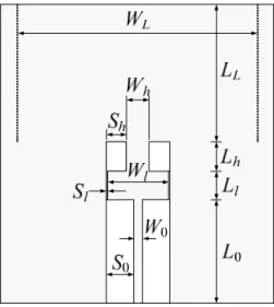
表一 使用偶極槽線天線的共面波導至矩形 波導功率分配器之尺寸。
(UNIT: MIL) Substrate: Rogers RT/Duroid 5880, 31 mil
L
875U
270g
15G
1 33.5W
120S
1 28G
73S
11表二 使用領結型槽線天線的共面波導至矩 形波導功率分配器之尺寸。
(UNIT: MIL) Substrate: Rogers RT/Duroid 5880, 31 mil
L
875U
246g
15G
1 33.5W
1 80S
1 28W
2 370G
73S
11出席國際學術會議心得報告
計畫編號 NSC 99-2221-E-011 -061
計畫名稱 寬頻共面波導至矩形波導功率分配器 出國人員姓名
服務機關及職稱
王蒼容
台灣科技大學 電子工程系 助理教授 會議時間地點 Oct. 23~Oct. 26, 2011, 美國 聖荷西
會議名稱 20th Conference on Electrical Performance of Electronic Packaging and Systems 2011 (EPEPS 2011)
發表論文題目
1. Bended Differential Transmission Line Using Short-Circuited Coupled Line for Common-Mode Noise Suppression
2. Compact Stepped-Impedance Resonator Transformer 一、參加會議經過
Oct. 24 (MON):
參加 EPEPS 2011 Power Integrity in High-Speed Designs 討論會。
參加 EPEPS 2011 Design Strategies for Processor, Chip/Package Co-design 討論會。
參加 EPEPS 2011 Novel RF and Chip-to-Chip Interconnects 討論會。
參加 EPEPS 2011 Macromodeling and Circuit Analysis 討論會。
參加 EPEPS 2011 Jitter Modeling and Analysis 討論會。
參加 EPEPS 2011 Poster Session,並在會議中發表我們的文章:
1. Bended Differential Transmission Line Using Short-Circuited Coupled Line for Common-Mode Noise Suppression
2. Compact Stepped-Impedance Resonator Transformer
Oct. 25 (TUE):
參加 EPEPS 2011 Measurements Methodologies for Signal Integrity 討論會。
參加 EPEPS 2011 Emerging Technologies: 3D ICs & Packages 討論會。
參加 EPEPS 2011 TSV Modeling 討論會。
參加 EPEPS 2011 Modeling and Simulation of MTLs 討論會。
參加 EPEPS 2011 Advanced Simulation Methodologies for SI Analysis 討論會。
參加 EPEPS 2011 High-Speed Links Design 討論會。
Oct. 26 (WED):
參加 EPEPS 2011 EM Methods for Variability Analysis 討論會。
參加 EPEPS 2011 Parallel EM Computing for Packages 討論會。
參加 EPEPS 2011 Advances in EM Algorithms 討論會。
二、與會心得
這次承蒙貴會補助,到美國聖荷西參加 20th Conference on Electrical Performance of Electronic Packaging and Systems 2011,在會議中發表論文並參與數場討論會,著實地令我獲 益良多。首先,我們在會議中發表自己的論文,展現我們創新的研究成果;在這個過程當中,
我們亦和相關領域的專家學者互相討論,並且接受專家的建議與指教,改良我們研究上的不 足之處,使我們的研究更加地精進。另外,除了本身的研究領域之外,我亦參加了數場討論 會,以瞭解其他研究領域的進展,並且從中吸收其他領域的知識。
除此之外,大會也舉辦了廠商展覽會,讓我們可以對產業界的趨勢有所的瞭解。這樣子 的安排,除了讓我們可以學習到專業的知識,也幫助我們瞭解產業界的動態。因此能夠參與 這次的會議,真的是相當的值得。
最後深切地感謝貴會的補助,讓這次的國際研討會可以成行,希望在未來的年度當中,
可以再度受到貴會的補助,讓我們的研究可以在國際上發表,並且從參與國際會議之中學習 到更多的新知,以充實我們的研究與產業知識。
September 2, 2011 Chun-Long Wang
No. 43, Sec. 4, Keelung Rd.
Taipei Taipei 106 Taiwan Dear Dr. Wang:
We are pleased to inform you that your papers entitled "Bended Differential Transmission Line
Using Short-Circuited Coupled Line for Common-Mode Noise Suppression" and “Compact Stepped-Impedance Resonator Transformer” have been accepted for presentation at the 2011
IEEE 20th Conference on Electrical Performance of Electronic Packaging Systems being held October 23-26, 2011 in San Jose, California and being administered by the University of Illinois.We also confirm the receipt of your registration information and fee. We look forward to your presentations in the conference.
If you need any additional information, please don’t hesitate to contact me.
Sincerely,
Mandy Wisehart EPEPS Administration
Bended Differential Transmission Line Using Short- Circuited Coupled Line for Common-Mode Noise
Suppression
Chia-Han Chang, Ruei-Ying Fang, and Chun-Long Wang
Department of Electronics Engineering, National Taiwan University of Science and Technology Taipei City, 106, Taiwan
[email protected], [email protected], and [email protected]
Abstract—In this paper, a bended differential transmission line using a short-circuited coupled line is proposed to efficiently suppress the common-mode noise. It has been shown that the bended differential transmission line using the short-circuited coupled line can greatly reduce the mode conversion from –5.47 dB to –14.75 dB and the TDT common-mode noise from 0.068 V to 0.02 V as compared with the bended differential transmission line using the right-angle bend. In order to verify the simulation results, measurement is done in the frequency and time domains where the measurement results are in good agreement with the simulation results.
Keywords-Compensation inductance; differential transmission line; common-mode noise; coupled line; shorted-end.
I. I
NTRODUCTIONDifferential signaling has been generally used in the high- speed digital interconnection on the PCBs, such as IEEE1394, USB 2.0, Serial ATA, and PCI-Express. In these applications, if the differential transmission line could maintain a symmetrical layout, the common-mode noise would not be induced. However, in practical circuit layouts, the differential transmission line may need to bend due to limited PCB space, which in turn results in an asymmetric structure. The asymmetric structure will then induce the common-mode noise when the differential signal passes through the asymmetric structure, leading to serious EMI and SI problems.
Some researchers have proposed various techniques to eliminate the common-mode noise [1]–[4]. At first, a common- mode suppression filter using periodically dumbbell-shaped defected ground structure (DGS) is proposed [1]. The periodically dumbbell-shaped DGS can filter out the common- mode noise without disturbing the differential-mode signal.
The advantage of this design is that it can be realized through the low cost PCB process but the drawback is that the size is so big that it will consume the available area in the ground plane.
In order to reduce the circuit size, the authors proposed another common-mode suppression filter by using two U-shaped and one H-shaped DGS [2]. This method has a broadband response and compact size but the area occupied is still about 0.44 λ
g× 0.44 λ
g. In order to further reduce the size, the authors use the multilayered LTCC process to realize a broadband and miniaturized common-mode filter [3]. The size of the filter is
further reduced to 0.16 λ
g× 0.26 λ
gbut there may be ground bounce problem since vias are used to penetrate the multilayered structure.
Other than the common-mode suppression filters mentioned previously, a bended differential transmission line using a compensation capacitance is proposed to eliminate the common-mode noise [4]. The compensation capacitance can then be implemented with a parallel plate capacitor, which conforms to the commonly-used PCB process. Besides, the circuit size of the parallel plate capacitor is approximately 0.10 λ
g× 0.10 λ
gat the center frequency of the interested frequency band.
In this paper, a bended differential transmission line using the short-circuited coupled line is proposed to eliminate the common-mode noise. Both the common-mode noise is greatly reduced and the circuit size is as small as that of the parallel- plate capacitor. In order to verify the simulation results, measurement is done both in the frequency and time domains where the measurement results are in good agreement with the simulation results.
II. B
ENDEDD
IFFERENTIALT
RANSMISSIONL
INEU
SINGR
IGHT-A
NGLEB
ENDA. Equivalent Circuit Model
The bended differential transmission line using the right- angle bend is shown in Fig. 1(a) along with the cross-sectional view shown in Fig. 1(b). The bended differential transmission line using the right-angle bend can be divided into three parts where the first and last parts denote the coupled transmission (Tx) lines and the middle part denotes the right-angle bend.
When the size of the right-angle bend is small as compared with the wavelength of the highest frequency of interest, the right-angle bend can be modeled by a lumped equivalent circuit model as shown in Fig. 1(c). As can be seen from Fig.
1(c), L
12and L
34denote the self inductances of the conducting wires; C
11, C
22, C
33, and C
44denote the self capacitances between the conducting wires and the ground plane; C
13, C
24, and L
mdenote the mutual capacitances and inductance between the conducting wires. Since the conductor and dielectric losses for the right-angle bend are small, their effects could be neglected.
This work was supported in part under the Grand NSC 99-2221-E-011-061 by National Science Council, Taiwan.
0 1 2 3 4 5 6 -70
-60 -50 -40 -30 -20 -10 0
Simulation (Full Wave)
Simulation (Model)
Mode Conversion (dB)
Frequency (GHz)
Fig. 2. Comparison between the simulated mode conversions of the full wave and model for the bended differential transmission lines using the right-angle bend.
The dimensions for the bended differential transmission line using the right-angle bend shown in Fig. 1(a) and (b) are w
= 1.75 mm, s = 0.75 mm, and l’ = 21.9948 mm. The substrate used is FR4 with a relative dielectric constant of ε
r= 4.3 and a thickness of h = 1.5 mm. Given the dimensions, the structure in Fig. 1(a) is simulated by Momentum and the simulation result is then used to extract the equivalent circuit parameters. The equivalent circuit parameters can be extracted through the procedures mentioned in the literature [4] where the extracted parameters are listed in Table I.
B. Differential-to-Common Mode Conversion
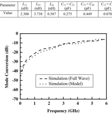
In order to investigate the differential-to-common mode conversion, Fig. 1(a) is simulated by Momentum to extract the four-port S parameters and then the four-port S parameters are converted to the mixed-mode S parameters [5]. The frequency responses of differential-to-common mode conversions for the bended differential transmission line using the right-angle bend shown in Fig. 1(a) and that using the equivalent circuit model shown in Fig. 1(c) are shown in Fig. 2. As can be seen from Fig. 2, the simulation result of Fig. 1 (a) is in good agreement with the simulation result of Fig. 1(c), and therefore the equivalent circuit model can properly represent the right-angle bend. Besides, it can be seen that the simulated differential-to- common mode conversions for Fig. 1(a) and Fig.1(c) are smaller than –5.47 dB and –6.07 dB, respectively, from DC to 6 GHz.
III. B
ENDEDD
IFFERENTIALT
RANSMISSIONL
INEU
SINGC
OMPENSATIONI
NDUCTANCEA. Design Rules
In order to eliminate the common-mode noise, the bended differential transmission line using the compensation inductance is proposed. By simply increasing the value of the inductance L
12in Fig. 1(c) to a value denoted by the compensation inductance, the common-mode noise can be greatly reduced. The value of the compensation inductance L
12can be calculated by
L12L342Zodd2 (C33C11)
(1) where L
12is the self inductance of the inner wire after compensation; L
34is the self inductance of the outer wire; C
11and C
22are the capacitances between the inner wire and the ground; Z
odddenotes the odd-mode impedance of the coupled Tx line. Equation (1) is derived by simply rearranging the formula for acquiring the compensation capacitance since the technique of using the compensation inductance is dual to the technique of using the compensation capacitance [4].
Given the equivalent circuit parameters of the right-angle bend, i.e. L
34= 3.738 nH, C
11= 0.275 pF, C
33= 0.449 pF, and Z
d= 49.7699 Ω as shown in Table I, the value of the compensation inductance L
12is calculated to be 4.600 nH through equation (1).
(a) (b)
(c)
Fig. 1. Bended differential transmission line using the right-angle bend. (a) Top view. (b) Cross-sectional view. (c) Equivalent circuit model.
TABLEI
EXTRACTED VALUES FOR THE EQUIVALENT CIRCUIT MODEL OF THE BENDED DIFFERENTIAL TRANSMISSION LINE USING RIGHT-ANGLE BEND
Parameter L12
(nH) L34
(nH) Lm
(nH) C11 = C22
(pF) C33 = C44
(pF) C13 = C24
(pF) Value 2.300 3.738 0.587 0.275 0.449 0.070
The equivalent circuit of the inner wire as shown in Fig.
1(c), which consists of the compensation inductance L
12along with the capacitances C
11and C
22, can then be implemented by a short-circuited coupled line as shown in Fig. 3. The parameters of the equivalent circuit of the inner wire and those of the short-circuited coupled line can be related by [6]–[7]
11
11 12 0
11 2 11 12
tan
2 o
Z Z j C jZ
C C
L
(2)
12
12 11 2 0 0
11 12
cot tan
2 2 e o
j
L j
Z Z Z
C C
L
(3)
where Z
0oand Z
0eare the odd- and even-mode impedances of the coupled line; θ is the electrical length of the coupled line.
By substituting the values of L
12and C
11into equations (2) and (3), and equating the equations at the frequency of 2 GHz, one set of (Z
0o, Z
0e) can be obtained by giving the electrical length θ = 19.78° as shown in the first three columns of Table II. By using LineCalc, these combinations of Z
0o, Z
0eand θ can then be transformed into the practical dimensions as shown in the last four columns of Table II where w
Land l
Lare the width and length of the coupled line, respectively, and s
Lis the space between the two wires of the coupled line.
B. Differential-to-Common Mode Conversion
By replacing the equivalent circuit of the inner wire in Fig.
1(c) with the short-circuited coupled line in Fig. 3, the layout
for the bended differential transmission line using the short- circuited coupled line can be realized as shown in Fig. 4 where the dimensions are shown in the second row of Table II.
The bended differential transmission line using the compensation inductance L
12as shown in Fig. 1(c) and that using the short-circuited coupled line as shown in Fig. 4 are simulated by using ADS. The simulated frequency responses of the differential-to-common mode conversion are shown in Fig. 5. As can be seen from Fig. 5, the mode conversion for the bended differential transmission line using the compensation inductance L
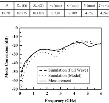
12and that using the short-circuited coupled line are below –15.59 dB and –14.75 dB, respectively.
It is clear that both the bended differential transmission line using the compensation inductance L
12and that using the short-circuited coupled line can effectively reduce the mode conversion.
In order to verify the simulation results, the bended differential transmission line using the short-circuited coupled line is fabricated on FR4 as shown Fig. 6. This circuit is then measured with Agilent/E5071B VNA after this equipment is calibrated with the N4431A electronic calibration kit where the measurement result is also shown in Fig. 5. As can be seen from Fig. 5, the measurement result is in good agreement with the simulation result, and the measured differential-to- common mode conversion is below –16.67 dB.
C. Time-Domain-Through Common-Mode Noise
Regarding the time domain simulation, the bended differential transmission line using the short-circuited coupled
Fig. 3. Schematic view of the short-circuited coupled line.
Fig. 4. Layout for the bended differential transmission line using the short- circuited coupled line.
TABLEII
PARAMETERS AND PRACTICAL DIMENSIONS OF SHORT-CIRCUITED COUPLED LINE
Z0o () Z0e () wL (mm) sL (mm) lL (mm) 2wL + sL
19.78° 89.275 103.889 0.730 2.789 4.762 4.249
0 1 2 3 4 5 6
-70 -60 -50 -40 -30 -20 -10 0
Simulation (Full Wave
)
Simulation (Model)
MeasurementMode Conversion (dB)
Frequrncy (GHz)
Fig. 5. Comparison between the simulation and measurement results of the mode conversions for the bended differential transmission lines using the short-circuited coupled line.
line shown in Fig. 4 is now simulated by using ADS where the driving source is a differential step function having a 0.5 volt amplitude with a rise time of 40 ps. The driving source is acquired from the waveform generated by the time-domain reflectometry (TDR) TEK/CSA8000 after the waveform has passed through two cables. It is noted that this driving source will include the cable loss, which will closely approximate the real source used in the measurement. The simulated TDT common-mode noise for the bended differential transmission line using the short-circuited coupled line is shown in Fig. 7 where the magnitude of the TDT common-mode noise is 0.02 V. Also shown in Fig. 7 is the simulated TDT common-mode noise for the bended differential transmission line using the right-angle bend, which is 0.068 V.
In order to verify the simulation result, Fig. 6 is measured in the time domain with TEK/CSA8000 where the measurement result is also shown in Fig. 7. As can be seen from Fig. 7, the simulation and measurement results are in good agreement where the magnitude of the measured TDT common-mode noise is 0.028 V. It is noted that the bended differential transmission line using the short-circuited coupled line can greatly reduce the differential-to-common mode conversion from –5.47 dB to –14.75 dB and the common- mode noise by (0.068 – 0.02)/0.068 = 70.5% as compared with the bended differential transmission line using the right- angle bend.
IV. C
ONCLUSIONIn order to eliminate the common-mode noise, a new bended differential transmission line using a short-circuited coupled line is proposed. The differential-to-common mode conversion for the bended differential transmission lines using the short-circuited coupled line is below –14.75 dB, which is much smaller than that for the bended differential transmission line using the right-angle bend. Besides, the TDT common- mode noise for the bended differential transmission line using the short-circuited coupled line is 0.02 V, which has 70.5%
reduction as compared with that of the bended differential transmission line using the right-angle bend.
Verifications are done both in the frequency and time domains where the measurement results are in good agreement with simulation results. Therefore, it is verified that the proposed structure could efficiently reduce mode conversion and the TDT common-mode noise at the receiving end.
A
CKNOWLEDGMENTThe authors would like to thank Prof. Ruey-Beei Wu, National Taiwan University, for providing the measurement instruments.
R
EFERENCES[1] W.-T. Liu, C.-H. Tsai, T.-W. Han, and T.-L. Wu, “An embedded common-mode suppression filter for GHz differential signals using periodic defected ground plane,” IEEE Microw. Wireless Compon. Lett., vol. 18, No. 4, pp. 248–250, Apr. 2008.
[2] S.-J. Wu, C.-H, Tsai, T.-L. Wu, and T. Itoh, “A novel wideband common-mode suppression filter for gigahertz differential signals using coupled patterned ground structure,” IEEE Trans. Microw. Theory Tech., vol. 57, no.4, pp. 848–855, Apr. 2009.
[3] C.-H. Tsai and T.-L. Wu, “A broadband and miniaturized common- mode filter for gigahertz differential signals based on negative- permittivity metamaterials,” IEEE Trans. Microw. Theory Tech., vol. 58, no.1, pp. 195–202, Jan. 2010.
[4] G.-H. Shiue, W.-D. Guo, C.-M. Lin, and R.-B. Wu, “Noise reduction using compensation capacitance for bend discontinuities of differential transmission lines,” IEEE Trans. Adv. Packag., vol. 29, pp. 560–569, Aug. 2006.
[5] W. Fan, A. Lu, L. L. Wai, and B. K. Lok, “Mixed-mode S-parameter characterization of differential structures,” in Proc. IEEE 5th Electron.
Packag. Technol. Conf., Dec. 2003, pp. 533–537.
[6] D. M. Pozar, Microwave Engineering, 3rd ed. New York: Wiley 2005.
[7] G. L. Matthaei, L. Young, and E. M. T. Jones, Microwave Filters, Impedance-Matching Networks, and Coupling Structures. Artech House, 1980.
Fig. 6. Photograph of the fabricated circuit for the bended differential transmission line using the short-circuited coupled line.
0.0 0.2 0.4 0.6 0.8 1.0
-0.05 0.00 0.05 0.10 0.15
Right-angle bend (Simulation)
Short-circuited coupled line (Simulation) Short-circuited coupled line (Measurement)
TDT Commom-Mode Noise (V)
Time (ns)
Fig. 7. Comparison between the simulated and measured TDT common-mode noise for the bended differential transmission line using the short-circuited coupled line and that using the right-angle bend.
1
Abstract—In this paper, a compact stepped-impedance resonator (SIR) transformer is proposed The implemented CB-CPW to SIW transition using the SIR transformer has shown a 50%
reduction in size with only 2.09% reduction in the 15-dB fractional bandwidth as compared with using the quarter-wavelength transformer.
Keywords-Conductor-backed coplanar waveguide (CB-CPW);
substrate integrated waveguide (SIW); quarter-wavelength transformer; stepped-impedance resonator (SIR); transition
I. I
NTRODUCTIONQuarter-wavelength transformers have been commonly used in microwave and millimeter-wave circuit designs. These designs include transition designs [1], antenna designs [2], and etc. However, since the electrical length of the quarter-wavelength transformer is of a quarter wavelength, it may occupy a broad area when it is implemented on the printed circuit boards. In order to miniaturize the size of the quarter-wavelength transformer, an SIR transformer by using the SIR concept is proposed. The SIR concept has been widely used in the designs of compact and high rejection band filters [3]–[8]. Therefore, by incorporating the design equation of the SIR [8] with the design theory of the multi-section transformer [9], the design theory of the SIR transformer can be formed.
In order to demonstrate the capability of the new SIR transformer, a CB-CPW to SIW transition using the SIR transformer is proposed. Besides, a CB-CPW to SIW transition using a quarter-wavelength transformer is simulated for
comparison. A back-to-back circuit is fabricated and measured where the measurement results agree with the simulation results.
II. T
RANSITIONU
SINGQ
UARTER-W
AVELENGTHT
RANSFORMERA. Quarter-wavelength transformer
A schematic view of the quarter-wavelength transformer is shown in Fig. 1 where θ denotes the electrical length and Z
qdenotes the characteristic impedance of the quarter-wavelength transformer.
The load impedance R
Land the characteristic impedance Z
0are arbitrarily chosen as 4.3 and 52 Ω, respectively. The characteristic impedance Z
qof the quarter-wavelength section is calculated to be 14.95 Ω through the geometric mean of the load impedance R
Land the characteristic impedance Z
0[9].
The center frequency f
0of the quarter-wavelength transformer is arbitrarily chosen to be 3.12 GHz at which the electrical length θ is π/2 (90
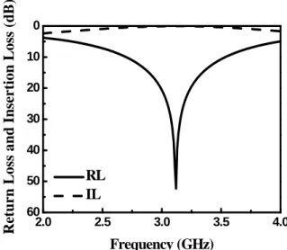
°). By simulating Fig. 1 with the commercial software ADS, the frequency response of the return and insertion losses are shown in Fig. 2. As can be seen from Fig. 2, the fractional bandwidth for which the return loss is larger than
Compact Stepped-Impedance Resonator Transformer
Ruei-Ying Fang, Chia-Fen Liu, and Chun-Long Wang
Department of Electronics Engineering, National Taiwan University of Science and Technology, Taipei City, 10607, Taiwan
[email protected], [email protected], and [email protected]
l
R
LZ
0Z
inZ
qFig. 1 A quarter-wavelength transformer.
θ
2.0 2.5 3.0 3.5 4.0
60 50 40 30 20 10 0
Re tur n Loss and Inse rti o n Loss (dB)
Frequency (GHz) RL
IL
Fig. 2 Frequency response of the quarter-wavelength transformer.
This work was supported in part under the Grand NSC
97-2221-E-011-022 by National Science Council, Taiwan.
2
15 dB is 14.74%.
B. CB-CPW to SIW transition using quarter-wavelength transformer
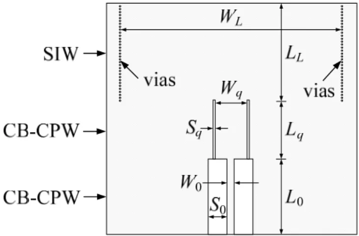
The quarter-wavelength transformer can then be implemented with a CB-CPW to SIW transition operating in S-band (2.60
–3.95 GHz) as shown in Fig. 3. As can be seen from Fig. 3, the characteristic impedance Z
0is realized as a 52.4-Ω CB-CPW; the quarter-wavelength transformer is realized as a 14.95-Ω quarter-wavelength CB-CPW; the load impedance R
Lis realized as a 4.3-Ω SIW. The reason why SIW is chosen to realize R
Lis that since the load impedance R
Lis so low, it is not easily to be implemented with CB-CPW.
The substrate used to realize these circuits is RT 5880, which has a thickness of 0.508 mm and a relative dielectric constant of 2.2. The dimensions of the CB-CPW to SIW transition using the quarter-wavelength transformer are listed in Table I. Besides, the diameter of the via is 0.3 mm and the distance between adjacent vias is 0.3 mm, which is limited by
the available fabrication process.
Fig. 3 is then simulated by using the commercial software HFSS and the resulting frequency responses of the return and insertion losses are shown in Fig. 4. As can be seen from Fig. 4, the 15-dB fractional bandwidth of the return loss is 25.86% in which the corresponding insertion loss is 0.2 dB. The center frequency f
0slightly move from 3.12 GHz to 3.48 GHz.
III. T
RANSITIONU
SINGS
TEPPED-I
MPEDANCER
ESONATORT
RANSFORMERA. Stepped-impedance resonator transformer
Reconsider Fig. 1 and assume that the characteristic impedance Z
0is greater than the load impedance R
L. In order to miniaturize the quarter-wavelength transformer, the quarter-wavelength transformer shown in Fig. 1 is replaced with a combination of low impedance line Z
lwith electrical length θ
land high impedance line Z
hwith electrical length θ
has shown in Fig. 5. In such an arrangement, Z
0will be much greater than Z
l, and Z
hwill be much greater than R
L.
In the design of the multi-section transformer, Γ
0is set equal to Γ
2in order to have a symmetrical structure [9]. By enforcing Γ
0= Γ
2, we have
0
h l L
Z Z Z R
. (1) Since Z
0is much greater than Z
land Z
his much greater than R
L, Fig. 5 can be approximated as an SIR where the minimum electrical length of the SIR resonator θ
T= θ
h+ θ
lcan be achieved by enforcing
tan-1 /
h l Z Zl h
(2)
[8]. Given the load impedance R
L= 4.3 Ω and the characteristic impedance Z
0= 52 Ω, the low impedance Z
land high impedance Z
hcan be calculated for various total electrical
Fig. 3 CB-CPW to SIW transition using the quarter-wavelength transformer.
TABLEI
DIMENSIONS OF THE CB-CPW TO SIWTRANSITION USING THE QUARTER-WAVELENGTH TRANSFORMER (UNIT: MM)
WL LL Wq Sq Lq W0 S0 L0
48.9 26.7 7.2 0.2 13 1.5 4 20
2.0 2.5 3.0 3.5 4.0
60 50 40 30 20 10 0
R et u rn Loss and Ins ertion Loss (dB)
Frequency (GHz) RL
IL
Fig. 4 Frequency responses of the return and insertion losses for the CB-CPW to SIW transition using the quarter-wavelength transformer.
Fig. 5 A stepped-impedance resonator transformer.
3
length θ
Tthrough equations (1) and (2) as listed in Table II.
Fig. 6 shows the frequency responses of the return losses for various electrical lengths θ
T, which are obtained by simulating Fig. 5 along with the first, second and third columns in Table II. As can be seen from Fig. 6, the center frequencies of the return losses deviate slightly even though the electrical length θ
Tchanges greatly. Furthermore, the 15-dB fractional bandwidth for various electrical lengths θ
Tare calculated and listed in the fourth column of Table II. As can be seen from Table II, when the total electrical length θ
Tof the SIR transformer is greatly reduced, which in turn saves the circuit size, the corresponding fractional bandwidth of the SIR transformer is slightly narrowed down as a tradeoff. For example, by comparing the case of θ
T= 60
°with that of θ
T= 90
°, the electrical length has a 33% reduction whereas the fractional bandwidth has only 2.14% reduction.
B. CB-CPW to SIW transition using stepped-impedance resonator transformer
The SIR transformer shown in Fig. 5 can then be implemented with a CB-CPW to SIW transition as shown in Fig. 7. As can be seen from Fig. 7, the characteristic impedance Z
0is realized as a 52.6-Ω CB-CPW. The high and low impedances Z
hand Z
lare realized as CB-CPWs; the load impedance R
Lis realized as a 4.3-Ω SIW. The dimensions of the CB-CPW to SIW transition corresponding to θ
T= 60
°in the fifth row of Table II are listed in Table III. In addition, the substrate used to realize these circuits and the dimensions of the vias are the same as those mentioned in Section II, B.
The frequency responses of the return and insertion losses for the CB-CPW to SIW transition using the SIR transformer is shown in Fig. 8. As can be seen from Fig. 8, the center frequency f
0is slightly shifted from 3.12 GHz to 3.45 GHz where the fractional bandwidth for which the return loss is larger than 15 dB is 23.77% and the corresponding insertion loss is smaller than 0.2 dB. As compared with the CB-CPW to SIW transition using the quarter-wavelength transformer, the total length (L
h+ L
l) of the CB-CPW to SIW transition using the SIR transformer is half the length (L
q) of the CB-CPW to
TABLEII
PARAMETERS OF THE SIRTRANSFORMER
θT High impedance Zh
(Ω)
Low impedance Zl
(Ω)
15-dB Fractional Bandwidth (%)
90° 14.95 14.95 14.74 80° 17.81 12.54 13.80 70° 21.35 10.47 13.22
60° 25.89 8.63 12.60
50° 32.00 6.97 12.52
2.0 2.5 3.0 3.5 4.0
60 50 40 30 20 10 0
Ret u rn Loss (d B )
Frequency (GHz)
Fig. 6 The frequency response of the return loss for various electrical lengths θT.
Fig. 7 CB-CPW to SIW transition using the SIR transformer.
2.0 2.5 3.0 3.5 4.0
60 50 40 30 20 10 0
Ret u rn Loss and Ins ert ion Loss (d B )
Frequency (GHz) RL
IL
Fig. 8 Frequency responses of the return and insertion losses for the CB-CPW to SIW transition using the SIR transformer with θT = 60°.
4
SIW transition using the quarter-wavelength transformer whereas the fractional bandwidth of the CB-CPW to SIW transition using the SIR has only 2.09% reduction from that of the CB-CPW to SIW transition using the quarter-wavelength transformer.
IV.
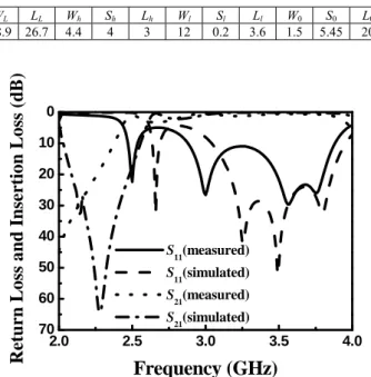
MEASUREMENT RESULTIn order to verify the simulation results, two CB-CPW to SIW transitions using the quarter-wavelength transformer are connected back-to-back and fabricated as shown in Fig. 9. The dimensions for this back-to-back transition are the same as those mentioned in Table I. The length of the L
back1in Fig. 9 is equal to 38.1 mm. The fabricated circuit is then measured with Anritsu 37347C VNA after it is calibrated with the TRL calibration kit. The measured insertion and return losses are shown in Fig. 10 along with the simulated insertion and return losses. As can be seen from Fig. 10, both the simulation and measurement results are in good agreement for both the insertion and return losses, which therefore verify our design.
V. C
ONCLUSIONIn this paper, an SIR transformer is proposed to miniaturize the quarter-wavelength transformer. In order to demonstrate the capability of the SIR transformer, the SIR transformer is implemented with the CB-CPW to SIW transition using the SIR transformer. The CB-CPW to SIW transition using the SIR transformer yields a 50% area reduction and a 2.09%
15-dB fractional bandwidth reduction as a tradeoff as compared with the CB-CPW to SIW transition using the quarter-wavelength transformer. In order to verify our simulation results, we fabricate a back-to-back CB-CPW to SIW transition using the quarter-wavelength transformer where the measurement results are in good agreement with the simulation results.
A
CKNOWLEDGMENTWe thank Chih-Lin Chang for assisting the TRL calibration and measurement. We also thank Prof. Chao-Hsiung Tseng for providing the measurement instruments.
R
EFERENCES[1] Y. Lou, C. H. Chan, and Q. Xue, “An in-line waveguide-to-microstrip transition using radial-shaped probe,” IEEE Microw. Wireless Compon.
Lett, vol. 18, no. 5, pp. 311–313, May 2008.
[2] C. H. Chang and K. L.Wong, “Quarter-wavelength printed loop antenna with an internal printed matching circuit for GSM/DCS/PCS/UMTS operation in the mobile phone,” IEEE Trans. Antennas Propag., vol. 57, no. 9, pp. 2541–2547, Sep. 2009.
[3] M. Makimoto and S. Yamashita, “Bandpass filters using parallel coupled stripline stepped impedance resonators,” IEEE Trans. Microw. Theory Tech., vol. MTT-28, no. 12, pp. 1413–1417, Dec. 1980.
[4] J.-T. Kuo, C.-L. Hsu, and E. Shih, “Compact planar quasi-elliptic function filter with inline stepped-impedance resonators,” IEEE Trans.
Microw. Theory Tech., vol. 55, no. 8, pp. 1747–1755, Aug. 2007.
[5] A.-S. Liu, T.-Y. Huang, and R.-B. Wu, “A dual wideband filter design using frequency mapping and stepped-impedance resonators,” IEEE Trans. Microw. Theory Tech., vol. 56, no. 12, pp. 2921–2929, Dec. 2008.
[6] S.-C. Lin, P.-H. Deng, Y.-S. Lin, C.-H. Wang, and C. H. Chen,
“Wide-stopband microstrip bandpass filters using dissimilar quarter-wavelength stepped-impedance resonators,” IEEE Trans.
Microw. Theory Tech., vol. 54, no. 3, pp. 1011–1018, Mar. 2006.
[7] S.-F. Chao, C.-H. Wu, Z.-M. Tsai, H. Wang, and C. H. Chen,
“Electronically switchable bandpass filters using loaded stepped-impedance resonators,” IEEE Trans. Microw. Theory Tech., vol.
54, no. 12, pp. 4193–4201, Dec. 2006.
[8] C. F. Chen, T. Y. Huang, and R. B. Wu, “Compact microstrip cross-coupled bandpass filters using miniaturized stepped impedance resonators,” in Proc. Asia–Pacific Microw. Conf., vol 1, pp 47, Dec.
2006.
[9] D. M. Pozar, Microwave Engineering, 3rd ed., New York: Wiley 2005.
TABLEIII
DIMENSIONS OF THE CB-CPW TO SIWTRANSITION USING THE SIR TRANSFORMER (unit: mm)
WL LL Wh Sh Lh Wl Sl Ll W0 S0 L0
48.9 26.7 4.4 4 3 12 0.2 3.6 1.5 5.45 20
2.0 2.5 3.0 3.5 4.0
70 60 50 40 30 20 10 0
R eturn Loss and Insertion Loss (d B)
Frequency (GHz)
S11(measured) S11(simulated) S21(measured) S21(simulated)
Fig. 10 Comparison between the simulation and measurement results for the CB-CPW to SIW transition using the quarter-wavelength transformer.
L
back1L
back1Fig. 9 Photograph of the fabricated circuit.
國科會補助計畫衍生研發成果推廣資料表
日期:2011/10/07
國科會補助計畫
計畫名稱: 寬頻共面波導至矩形波導功率分配器 計畫主持人: 王蒼容
計畫編號: 99-2221-E-011-061- 學門領域: 電磁
無研發成果推廣資料