Growth and Characterization of Sparsely Dispersed ZnO
Nanowires
Ting-Jen Hsueh,aCheng-Liang Hsu,bShoou-Jinn Chang,aYan-Ru Lin,c Tzer-Shen Lin,dand I-Cherng Chene,z
a
Institute of Microelectronics and Department of Electrical Engineering, National Cheng Kung University, Tainan 70101, Taiwan
b
Department of Electronic Engineering, National University of Tainan, Tainan 700, Taiwan c
Photovoltaics Technology Center, Industrial Technology Research Institute, Chutung, Hsinchu 31040, Taiwan
d
Material and Chemical Research Laboratories, Industrial Technology Research Institute, Chutung, Hsinchu 31040, Taiwan
e
Micro Systems Technology Center, Industrial Technology Research Institute South, Tainan, 709, Taiwan
This investigation describes the growth of sparsely dispersed vertical ZnO nanowires on sputtered-ZnO:Ga/sapphire templates by self-catalyzed vapor liquid solid method. Experimental results indicate that these ZnO nanowires grew with the preferred共002兲 orientation with good crystal quality. Conductive diamond-coated point probe forms Schottky contact on single ZnO nanowire with a sharp turn-on voltage of⬃2.5 V and a barrier height of approximately 0.38 eV.
© 2007 The Electrochemical Society. 关DOI: 10.1149/1.2424415兴 All rights reserved. Manuscript submitted September 13, 2006; revised manuscript received October 23, 2006. Available electronically January 5, 2007.
Much attention has focused on the improvement of growth meth-ods and the optical characteristics of wide bandgap semiconductors to develop high-performance short wavelength photonic devices, such as light emitters and photodetectors. Various wide bandgap semiconductors, including such as 6H–SiC and GaN, have been in-tensively investigated in the past decade.1-3 Zinc oxide 共ZnO兲 is another potentially useful wide bandgap semiconductor material. ZnO is an n-type II-VI wide bandgap compound semiconductor with a hexagonal wurtzite structure and a high melting temperature.4,5 ZnO also has a strong exciton binding energy of 60 meV, which is much larger than those of conventional compound semiconductors such as GaAs共5 meV兲, ZnSe 共19 meV兲 and GaN 共24 meV兲.6Such a large exciton binding energy makes ZnO a promising photonic material for various applications. Indeed, high-quality ZnO epitaxial thin films and optical devices based on these thin films have already been demonstrated.4 One-dimensional 共1D兲 ZnO nanowires have also been synthesized. One-dimensional nanowires are potentially useful for applications in nanoscale optoelectronic, piezoelectric and mechanical devices.7,8For example, 1D photodetectors can provide a stronger photoresponse because their aspect ratio length to diam-eter and surface to volume ratio are higher than those of the bulk or thin film photodetectors. To our knowledge, ZnO 1D nanowires can be synthesized by various techniques, such as chemical vapor deposition,9template-assisted growth,10 solution-based synthesis,11 catalyst-driven molecular beam epitaxy,12metallorganic vapor phase epitaxy,13,14vapor-liquid-solid共VLS兲 methods15,16and catalyst-free growth by thermal evaporation.17-19 Very recently, Hsu et al. re-ported the growth of ZnO nanowires on ZnO:Ga/glass templates by self-catalyzed VLS method.20The effects of the growth parameters have also been reported.21,22 Self-catalyzed VLS can be used to produce high-density vertical well-aligned ZnO nanowires. How-ever, elucidating the details of the growth mechanism of a single ZnO nanowire is difficult. This study reports the growth of sparsely dispersed ZnO nanowires on sapphire substrates by two-step oxygen injection in self-catalyzed VLS, without any metal catalyst.23The details of the growth procedure of sparsely dispersed ZnO nano-wires is discussed. The physical and electrical properties of the de-posited ZnO nanowires is also discussed.
Experimental
Prior to the growth of ZnO nanowires, 50 nm thick electrically conductive Ga-doped ZnO thin films were deposited onto sapphire
substrates by radio frequency magnetron sputtering. During the deposition of the ZnO:Ga thin films, the flow rates of O2/Ar, the
substrate temperature, the distance between the target and the sub-strate, the sputtering power, the deposition time and the chamber pressure were 30/30 sccm, 250°C, 12 cm, 400 W, 20 min and 10 mTorr, respectively. X-ray diffraction共XRD兲 indicated that the deposited ZnO:Ga film was oriented in the共002兲 direction. The zinc vapor source for the growth of ZnO nanowires was Zn metal powder with a purity of 99.9%, obtained from Strem Chemicals. ZnO:Ga/ sapphire template and Zn powder were then loaded onto an alumina boat and inserted into a quartz tube. The evaporation was performed in the quartz tube in a horizontal tube furnace. Argon and oxygen gases were then introduced into the reaction system. The argon flow rate and the chamber pressure were kept at 54.4 sccm and 10 Torr, respectively, throughout the growth. The growth of ZnO nanowires proceeded in two steps. In the first step, the temperature was ramped up at 30°C/min. Initially, only Ar was introduced into the furnace. When the temperature reached 450°C, the oxygen gas began to be poured into the chamber at a flow rate of 0.8 sccm. When the tem-perature reached 600°C, the temtem-perature ramping process was ter-minated and the chamber temperature was maintained at 600°C to grow the ZnO nanowires continuously. The total growth time was 20 min.
An MAC MXP18 X-ray diffractometer共XRD兲 was then used to characterize the samples. The surface morphology of the samples was characterized by a JEOL JSM-6500F field emission surface electron microscope 共SEM兲, operated at 5 keV. Cathodolumines-cence共CL兲 was applied to evaluate the quality of the deposited ZnO nanowires. During CL measurements, the electron beam power was maintained at 1.62 W. 共The electrons were accelerated at 30 kV with an emission current of 81A.兲 Current-voltage 共I-V兲 charac-teristics of the fabricated ZnO nanowires were then measured using an SII SPA-300HV scanning probes microscope共SPM兲 with a con-ductive diamond-coated point probe共CDT-NCHR, Nanosensor兲 in contact mode. The current limit of the SPM system was 100 pA and the diameter of the conductive diamond-coated point probe was 100–200 nm.
Results and Discussion
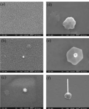
Since oxygen gas was introduced into the chamber when the temperature reached 450°C, ZnO nanowires started to grow at this temperature共0 min兲. A series of SEM micrographs are obtained to clarify the growth mechanism of the ZnO nanowires. Figure 1a shows a top-view SEM micrograph of the sputtered ZnO:Ga film
zE-mail: [email protected]
Journal of The Electrochemical Society, 154共3兲 H153-H156 共2007兲
0013-4651/2007/154共3兲/H153/4/$20.00 © The Electrochemical Society H153
without ZnO nanowires. The sputtered ZnO:Ga thin film was poly-crystalline with a reasonably smooth surface. Figures 1b-d show top-view SEM micrographs of a single ZnO nanowire, photo-graphed at 1.5, 3 and 4.5 min., respectively. As shown in Fig. 1b, Zn droplets react with O2 to initiate the nucleation of ZnO nanowire
after O2gas was introduced and the temperature was increased
sta-bly for 1.5 min. After 3 min, the nucleated ZnO nanowire continued to adsorb oxygen to reach the supersaturation state. The hexagonal wurtzite structure of ZnO was clearly observed as the temperature was increased. As shown in Fig. 1d, a pyramid-like ZnO structure was formed after 4.5 min. Figures 1e and f show top-view and 30°-tilted SEM micrographs, respectively, of the single ZnO nanowire, photographed at 20 min. Clearly, a vertical ZnO nanowire was grown directly on top of the pyramid-like ZnO structure. Further-more, the length and diameter of the as-grown ZnO nanowires were around 1.2m and 90 nm, respectively. Figure 2 summarizes the results obtained from these six SEM micrographs.
The sputtered-ZnO:Ga/sapphire template was loaded into our furnace without the Zn powder to clarify the growth mechanism of the ZnO nanowires. The sputtered-ZnO:Ga/sapphire template was heat-treated with only Ar gas. Figure 3 shows a top-view SEM mi-crograph of the sputtered-ZnO/sapphire template that was heat-treated with neither O2gas nor Zn powder. A comparison with the
micrograph shown in Fig. 1a reveals that sparse defects were gen-erated on the surface of the sputtered ZnO:Ga film. With the small activation energy, these sparse defects may serve as the nucleation sites. The melting point of Zn is around 420°C. When the tempera-ture rises above 420°C, the Zn vapor pressure inside the furnace should increase rapidly共The saturation steam pressure was around 0.1667 Torr.兲 Thus, some of the zinc metal power will be volatilized prior to the introduction of oxygen at around 450°C. As the tem-perature is increased further, the ZnO epitaxial layer begins to grow homoepitaxially on the sputtered ZnO:Ga film. However, lattice mismatch between ZnO and sapphire-induced defects will be gener-ated at the ZnO surface as the thickness of ZnO film increases. These defects serve as the nucleation sites for the subsequent growth of ZnO nanostructures. Restated, ZnO begins to nucleate and to form the pyramid-like ZnO structure. Since the underlying sputtered ZnO thin film was oriented in the共002兲 direction, the growth rate of ZnO nanowires along the c axis should exceed that of other pris-matic sides. Sparsely dispersed vertical ZnO nanowires can thus be achieved, as shown in Fig. 1e and f. Figure 4a shows the measured XRD spectrum of the sputtered ZnO:Ga film without ZnO nano-wires while Fig. 4b shows the measured XRD spectrum of the ZnO nanowire sample, shown in Fig. 1b. These samples yielded both ZnO共0002兲 and sapphire 共0006兲 XRD peaks. The relative intensity
Figure 1. Top-view SEM micrographs of共a兲 sputtered ZnO:Ga films without ZnO nanowires,共b兲 single ZnO nanowire grown for 1.5 min, 共c兲 single ZnO nanowire grown for 3 min,共d兲 single ZnO nanowire grown for 4.5 min, 共e兲 single ZnO nanowire grown for 20 min. Figure e shows 30°-tilted SEM micrographs of a single ZnO nanowire grown for 20 min.
Figure 2. Summary of the results presented in Fig. 1a-f.
Figure 3. Top-view SEM micrograph of the sputtered-ZnO:Ga/sapphire tem-plate heat-treated with neither O2nor Zn powder.
Figure 4.共Color online兲 XRD spectra measured at room temperature for 共a兲 sputtered-ZnO:Ga/sapphire sample, and共b兲 ZnO nanowires and epitaxial-ZnO/sputtered-ZnO:Ga/sapphire sample.
H154 Journal of The Electrochemical Society, 154共3兲 H153-H156 共2007兲
H154
of the ZnO peak from the ZnO nanowire sample was larger. This observation also indicates that the ZnO nanowires were grown along the c axis of ZnO关0002兴. The extremely narrow XRD line shown in Fig. 4b also suggests the good crystal quality of our nanowires.20,22
The VLS method is a well-known and commonly used method for growing nanowires.23It uses nanosized metal clusters as a cata-lyst to absorb gas phase reactants and to form eutectic alloy droplets. As the reactant in the liquidized droplets becomes super saturated, precipitation begins and the 1D nanowires will be formed. Notably, nanoparticles are always present at the tip of the 1D nanowires prepared by VLS method. In this experiment, however, no transition metal was used as a catalyst during growth. Furthermore, no addi-tional metal particle was found on top of the nanowires. Restated, the growth mechanism should differ from that of the conventional metal-catalytic VLS method. Other groups have reported the similar self-catalyzed VLS growth of ZnO nanowires.24,25Also, since the ZnO nanowires were sparsely dispersed, a single nanowire could be characterized. Figure 5 shows the cross-sectional CL panchromatic image of a single ZnO nanowire grown on a sputtered-ZnO:Ga/ sapphire template. The observed clearly uniform single nanowire image again suggests the good crystal quality of the ZnO nanowires. A 1.8 µm thick photo resist AZ 1500 was spin coated on top of the ZnO nanowires, and then baked for 3 min at 120°C to evaluate the electrical properties of the as-grown ZnO nanowires. The sample in diluted acetone共acetone: water = 1: 1兲 is etched for 1 min. Figure 6a shows a top-view SEM micrograph of the sample. The tips of the sparsely dispersed vertical ZnO nanowires could only be observed after etching. A SPM was then used to characterize the sample. Figure 6b shows a SPM image of a single ZnO single nanowire. The tip diameter of this single ZnO nanowire was around 90 nm. SPM was also used to evaluate I-V characteristics of this single ZnO nanowire. Figure 6c schematically depicts the 90 nm. SPM was also used to evaluate I-V measurement. Notably, photoresist AZ 1500 is
Figure 5. Cross-sectional CL image of a single ZnO nanowire grown on sputtered-ZnO:Ga/sapphire template.
Figure 6. 共Color online兲 共a兲 Top-view SEM micrograph and共b兲 SPM image of a single ZnO nanowire coated with photore-sist; 共c兲 schematic I-V measurement; 共d兲 measured I-V characteristic of single ZnO nanowire using diamond-coated point probe as the top contact.
H155
Journal of The Electrochemical Society, 154共3兲 H153-H156 共2007兲 H155
insulating. However, the resistances of the sputtered ZnO:Ga thin film共around 1 k⍀兲 and the bottom contact electrode 共around 1 k⍀兲 were both much smaller than that of the undoped ZnO nanowire 共⬎1 M⍀兲. Thus, the resistances of the bottom contact electrode and the sputtered ZnO:Ga thin film are negligible. Figure 6d plots mea-sured I-V characteristics of the single ZnO nanowire with a diamond-coated point probe used as the top contact. An asymmetri-cal Schottky-like rectifying behavior was formed with a sharp turn-on voltage of ⬃2.5 V and a reverse breakdown voltage of larger than 5 V. Since the diameter of the conductive diamond-coated point probe was 100⬃ 200 nm, the electric field was uni-formly spread on top of the single ZnO nanowire. Thus, the tunnel-ing current between the diamond-coated point probe and the ZnO nanowire could be minimized. Restated, the dark forward current observed in Fig. 6d should be dominated by thermionic emission. Thermionic emission theory demonstrates the Schottky barrier height26
Is= AA*T2exp
冉
−eb0
kT
冊
关1兴where Isis the saturation current, k is the Boltzmann constant, T is the absolute temperature, A is the Schottky contact area, A* = 4qm*k2h−3is the effective Richardson constant, and
b0is the
zero-biased Schottky barrier height. The electron effective mass
me*= 0.27 m0reported by Sze indicates that the effective Richard-son constant of ZnO A*= 32 A cm2K−2.27However, the electron effective mass and effective Richardson constant of ZnO are still under debate. For example, Sheng et al.28measured current-voltage temperature共I-V-T兲 to determine the Schottky barrier height of Ag on ZnO, and found that A*= 0.15 A cm−2K−2. They attributed the
smaller A*to the electrons29
tunneling through an inhomogeneous barrier. However, Oshikiri et al.29measured cyclotron resonance and found that the electron effective mass of ZnO, me*= 0.23 m0, which is close to the theoretically calculated value me*= 0.24 m0. More recently, Meyer et al. reported an electron effective mass of ZnO of 0.28m0in the direction parallel to the c axis and a value of 0.24 m0
in the direction perpendicular to the c axis.30Since the tunneling current is negligible in this study, me*= 0.27 m0 and A*
= 32 A cm−2K−2are used. The data shown in Fig. 6d and Eq. 1
indicate that the Schottky barrier height between the diamond-coated point probe and the undoped ZnO nanowire was 0.38 eV at room temperature.
Conclusions
In summary, sparsely dispersed vertical ZnO nanowires were prepared on sputtered-ZnO:Ga/sapphire templates by the self-catalyzed VLS method. The growth mechanism of the ZnO nano-wires was investigated by SEM. The length and diameter of the as-grown ZnO nanowires were around 1.2m and 90 nm,
respec-tively. These ZnO nanowires were grown with the preferred共002兲 orientation with good crystal quality. Furthermore, the diamond-coated point probe forms a Schottky contact on single ZnO nano-wire, with a sharp turn-on voltage of⬃2.5 V and a barrier height of around 0.38 eV.
Industrial Technology Research Institute South assisted in meeting the publication costs of this article.
References 1. D. C. Look, Mater. Sci. Eng., B, 80, 383共2001兲.
2. C. H. Liu, C. S. Chang, S. J. Chang, Y. K. Su, Y. Z. Chiou, S. H. Liu, and B. R. Huang, Mater. Sci. Eng., B, 100, 142共2003兲.
3. S. J. Chang, T. K. Ko, Y. K. Su, Y. Z. Chiou, C. S. Chang, S. C. Shei, J. K. Sheu, W. C. Lai, Y. C. Lin, W. S. Chen, and C. F. Shen, IEEE Sens. J., 6, 406共2006兲. 4. T. K. Lin, S. J. Chang, Y. K. Su, B. R. Huang, M. Fujita, and Y. Horikoshi, J. Cryst.
Growth, 281, 513共2005兲.
5. J. Yahiro, Y. Oaki, and H. Imai, Small, 2, 1183共2006兲.
6. H. J. Ko, S. K. Hong, Y. Chen, and T. Yao, Thin Solid Films, 409, 153共2002兲. 7. H. Kind, H. Yang, B. Messer, M. Law, and P. Yang, Adv. Mater. (Weinheim, Ger.),
14, 158共2002兲.
8. H. J. Fan, W. Lee, R. Hauschild, M. Alexe, G. L. Rhun, R. Scholz, A. Dadgar, K. Nielsch, H. Kalt, A. Krost, M. Zacharias, and U. Gosels, Small, 2, 561共2006兲. 9. J. Wu and S. Liu, J. Phys. Chem. B, 106, 9546共2002兲.
10. Y. Li, G. W. Meng, L. D. Zhang, and F. Phillipp, Appl. Phys. Lett., 76, 2011 共2000兲.
11. L. Vayssieres, Adv. Mater. (Weinheim, Ger.), 15, 464共2003兲.
12. Y. W. Heo, V. Varadarajan, M. Kaufman, K. Kim, D. P. Norton, F. Ren, and P. H. Fleming, Appl. Phys. Lett., 81, 3046共2002兲.
13. W. I. Park, Y. H. Jun, S. W. Jung, and G. C. Yi, Appl. Phys. Lett., 82, 964共2003兲. 14. S. Muthukumar, H. Sheng, J. Zhong, Z. Zhang, N. W. Emanaetoglu, and Y. Lu,
IEEE Trans. Nanotechnol., 2, 50共2003兲.
15. M. H. Huang, Y. Wu, H. Feick, N. Tran, E. Weber, and P. Yang, Adv. Mater.
(Weinheim, Ger.), 13, 113共2000兲.
16. C. Geng, Y. Jiang, Y. Yao, X. Meng, J. A. Zapien, C. S. Lee, Y. Lifshitz, and S. T. Lee, Adv. Funct. Mater., 14, 589共2004兲.
17. J. Grabowska, K. K. Nanda, E. McGlynn, J. P. Mosnier, and M. O. Henry, Surf.
Coat. Technol., 200, 1093共2005兲.
18. W. Lee, M. C. Jeong, and J. M. Myoung, Nanotechnology, 15, 1441共2004兲. 19. T. J. Hsueh, S. J. Chang, Y. R. Lin, S. Y. Tsai, I. C. Chen, and C. L. Hsu, Cryst.
Growth Des., 6, 1282共2006兲.
20. C. L. Hsu, S. J. Chang, Y. K. Tseng, C. J. Huang, H. M. Cheng, and I. C. Chen,
IEEE Trans. Nanotechnol., 4, 649共2005兲.
21. Y. K. Tseng, H. C. Hsu, W. F. Hsieh, K. S. Liu, and I. C. Chen, J. Mater. Res., 18, 2837共2003兲.
22. C. L. Hsu, S. J. Chang, H. C. Hung, Y. R. Lin, T. H. Lu, Y. K. Tseng, and I. C. Chen, J. Vac. Sci. Technol. B, 23, 2292共2005兲.
23. P. Yang, Proc. SPIE, 4806, 222共2002兲.
24. J. Q. Hu, Q. Li, N. B. Wong, C. S. Lee, and S. T. Lee, Chem. Mater., 14, 1216 共2002兲.
25. B. D. Yao, Y. F. Chan, and N. Wang, Appl. Phys. Lett., 81, 757共2002兲. 26. S. H. Kim, H. K. Kim, and T. Y. Seong, Appl. Phys. Lett., 86, 112101–1共2005兲. 27. S. M. Sze, Physics of Semiconductor Devices, p. 849, Wiley, New York共1981兲. 28. H. Sheng, S. Muthukumar, N. W. Emanetoglu, and Y. Lu, Appl. Phys. Lett., 80,
2132共2002兲.
29. M. Oshikiri, Y. Imanaka, F. Aryasetiawan, and G. Kido, Physica B, 298, 472 共2001兲.
30. B. K. Meyer, H. Alves, D. M. Hofmann, W. Kriegseis, D. Forster, F. Bertram, J. Christen, A. Hoffmann, M. Straßburg, M. Dworzak, U. Haboeck, and A. V. Rodina,
Phys. Status Solidi B, 241, 231共2004兲.
H156 Journal of The Electrochemical Society, 154共3兲 H153-H156 共2007兲
H156