A DC-DC Converter with Wide Input Voltage Range for Fuel Cell and Supercapacitor Application
Zhe Zhang, Ole C. Thomsen and Michael A. E. Andersen Department of Electrical Engineering
Technical University of Denmark Kgs. Lyngby, Denmark, DK2800
[email protected]
Abstract — This paper proposes a novel phase-shift plus duty cycle controlled hybrid bi-directional DC-DC converter based on fuel cells and supercapacitors. The described converter employs two high frequency transformers to couple the half-bridge and full-bridge circuits together in the primary side and voltage doubler circuit in secondary side. Boost type converter can limit the output ripple current of the fuel cells; hybrid full-bridge structure can change operating modes according to the different input voltage; phase-shift with duty cycle control scheme is utilized to control the bidirectional power flow flexibly. All the switches can turn on under zero-voltage-switching condition (ZVS). The operating principles of the converter are described in details, and the experimental results based on the prototype controlled by DSP are presented to verify the validity of the analysis and design.
Keywords-converter; dc-dc; bidirectional; soft-switching I. I NTRODUCTION
Nowadays, the hybrid system based on fuel cells (FCs) and supercapaciotrs (SCs) as an environmentally renewable energy system has been applied in many fields, such as hybrid electric vehicle (HEV), uninterruptible power supply (UPS) and so on.
Fuel cells can convert the chemical potential of the hydrogen into electric power directly, with consequent high conversion efficiency and possibility to obtain the extended range with the combustible feed from the outside [1]. But one of the main weak points of the fuel cell is its slow dynamics because of the limitation of hydrogen delivery system. So during the fuel cells warming up or load requirement transient, the supercapacitors can be utilized as the auxiliary power source for smoothing output power. On the other hand, because the fuel cell output voltage varying widely, almost 2:1, depending on different load conditions, and the terminal voltage of supercapacitors bank is variable during charging and discharging periods, it is very important for the conversion system to be capable of harvesting power from different power sources and have good performance in widely variable input voltage range and load variations. Many hybrid system structures have been proposed, and they can be divided into four categories: DC bus structure [2], [3], transformer-coupled structure [4], [5], [6], multi-port structure [7] and multi-stage structure, [8], [9]. For the DC bus structure, each power source is connected by a separate converter to the common voltage DC bus. In this architecture, each subsystem could be design as an individual module, but the complicated control is the main disadvantage. In high
frequency transformer coupled system, transformer design and power flow control are the keys to decide the performance of the system. For the multi-stage structure, efficiency is limited by the cascaded converters.
It is proposed that a novel DC-DC converter, as shown in Fig. 1, with fuel cells as main input power source and supercapacitors are connected directly to the low voltage side in this paper. The converter utilizes the boost-type input structure to limit the ripple current of the FCs [10] and hybrid full-bridge structure [11], [12] to change operating modes in terms of the different input voltage values. Phase-shift plus duty cycle modulation scheme can control the bidirectional power flow flexibly. This paper is organized into five sections.
Section II gives the operation principle of the proposed converter; Theoretical analysis, calculation and design results are present in Section III. Section VI shows the experimental results. Section V gives the conclusions.
II. O PERATION P RINCIPLES
As seen through Fig, 1, the boost type half bridge high frequency inverter with the switches operating by 50% duty cycle is in the primary side of the transformer, and supercapacitors C
SC1and C
SC2connect on the variable low voltage DC bus as the secondary energy source. S
3and S
4are controlled by duty-cycle, d, to change the operating modes, when input voltage is variable in the wide range. Two transformers, T
1and T
2, with the paralleled primary windings and series-wound secondary windings are utilized to realize isolation and boost the low input voltage. Voltage doubler circuit in secondary side of the transformer is to get higher voltage conversion ratio. The leakage inductances of the transformers are the interface and energy transfer elements between the two high frequency inverters.
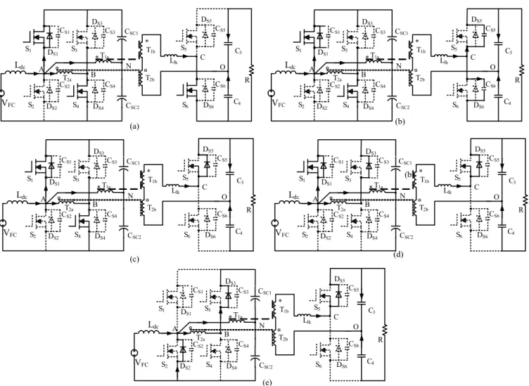
Fig1. Hybrid bidirectional dc-dc converter topology.
According to different power flow directions, operational modes of the proposed converter can be divided into two modes, Boost mode and Buck mode. In Boost mode, the power is delivered from the fuel cells and supercapacitors to the high voltage DC bus, which means energy is from low voltage side to the high voltage side. The counterpart is defined as Buck mode. In different modes, Boost or Buck, there are several sub- modes as well depending on different input or output voltage value to limit the peak currents of the converter, respectively.
The detailed operational modes are described as follows.
A. Boost mode
In Boost mode, when input voltage is around 30 V, S
1, S
4and S
2, S
3will turn on synchronously. Phase-shift modulation is used to control the power delivered, as shown in Fig. 2. When the input voltage is higher than 30 V, the converter will work under the multi-level operation sub-mode to limit the rms current value in the primary side of the transformers, through the duty cycle control on S
3and S
4, as shown in Fig. 3. If the output voltage, V
O, is controlled well, that means it can be seen as constant, we can define d as:
4 ) 1 ( 2 2
1 3
O FC s
on S
V n
v T
d T
⋅
− ⋅
⋅
=
⋅
= π π (rad) (1) Where n
1is turn ratio of the transformer T
1.
Because the 2-level operation is one special condition (duty cycle of S
3and S
4equal to 0.5) of the multi-level mode, only the multi-level sub-mode is analyzed in this paper. For the convenience of analysis, the following assumptions are given:
(1) all the switches are ideal with anti-parallel body diodes and parasitic capacitors; (2) The inductance L
dcis large enough to be treated as a current source; (3) Output voltage is controlled well which can be seen constant; (4) The two transformers are ideal and with series leakage inductor L
lkin the secondary side.
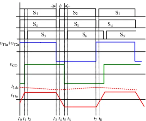
One complete switching cycle can be divided into ten intervals as shown in Fig. 3, and because of the similarity, only a half switching cycle in described in detail. The equivalent circuits are shown in Fig. 4.
1) Interval 1 (t
0-t
1): S
1, S
4and S
6are conducting. The voltage on L
lk, v
Llk, is v T 1 b + v T 2 b + V CO , so the i
Llkwill increase linearly. I
Ldcgoes though D
S1.
2) Interval 2 (t
1-t
2): at t
1, S
6is turned off. L
lk, C
S5and C
S6begin to resonate, C
S5is discharged and C
S6is charged. When voltage on C
S5reduces to zero, the anti-paralleled diode of S
5start to conduct, and the voltage v
COchanges the direction. So v
Llkequals to v T 1 b + v T 2 b − V CO .
3) Interval 3 (t
2-t
3): at t
2, S
5is turned on under ZVS. The current paths are same with these in Interval 2.
4) Interval 4 (t
3-t
4): at t
3, S
4is turned off. L
lk, C
S3and C
S4begin to resonate. When the voltage cross S
3reduces to zero, D
S3is therefore forward based. The voltage cross the primary winding of T
2is clamped to zero. So v
Llkequals to
CO b
T V
v 1 − .
5) Interval 5 (t
4-t
5): at t
4, S
1is turned off. L
lk, C
S1and C
S2begin to resonate. C
S2is discharged from 2V
FC. The rate of change depends on the magnitude i
T1a+i
T2a-I
Ldc. At t
5, v
CS2.Figure 2: Key waveforms in Boost mode with two voltage levels.
Figure 3: Key waveforms in Boost mode with three voltage levels.
Figure 5: Key waveforms in Buck mode with two voltage levels.
Figure 6: Key waveforms in Buck mode with three voltage levels.
attempts to overshoot the negative rail. D
S2is forward biased.
During this period, S
2can be turned on under ZVS.
After t
5, the second half cycle starts which is similar to the first half cycle.
B. Buck mode
The function of bidirectional power flow is necessary for charging the supercapacitors in Buck mode. Due to the reversed power-flow direction, the gate drive signal of S
5is leading to that of S
1, as shown in Fig. 5. During the charging process, the voltage on the supercapacitors is increased, so the phase-shift plus duty cycle control is utilized in Buck mode.
Because the half-bridge topology of the two sides is symmetrical, the operation principles in buck mode are similar to those in boost mode. But the fuel cells can not take the negative current, so there is no I
Ldcin Fig. 5 and Fig. 6. The Buck mode operation can also be divided into ten stages, and the description of each step can be analogously inferred and will not be discussed here.
C. Fuel cells warm-up stage
During the warm-up stage of the fuel cells, there is no output power from fuel cell yet, so there is no I
dcwaveform in Fig. 3. , but the operation principles are similar with that in Boost mode.
In this period, supercapacitors are discharged to deliver the energy stored to the load. The terminal voltage cross the SCs is reduced. To limit the peak current, extend the ZVS range and improve efficiency in this stage, the phase-shift with duty cycle control is used as analyzed above, so the converter is operated in three-level operation mode.
III. C HARACTERISTICS OF THE N OVEL C ONVERTER A. Output power
The phase shift angle δ ( − 0 . 5 π ≤ δ ≤ 0 . 5 π ), which is defined as shown in Fig. 2 and Fig. 3, is used to control the magnitude and direction of the transmitted power in two-level sub-modes. The output power is similar with what described in [10] and [13], shown as:
( π δ )
πω ⋅ δ −
= ⋅
lk H L
L V P 2 V
(1)
where V is the peak voltage value of the transformer L secondary side, v T 1 b + v T 2 b ; V is the peak voltage value of H
v CO ; ω is the switching angular frequency.
A S1
S2
B N
T2a T2b
T1a T1b
CSC1
CSC2
L
dcS3
S4
S5
S6
O
V
FCC3
C4
R Llk C
*
* DS1
CS1
DS2
CS2
DS3
CS3
DS4
CS4
DS5
CS5
DS6
CS6
A S1
S2
B N
T2a T2b
T1a
T1b
CSC1
CSC2
L
dcS3
S4
S5
S6
O
V
FCC3
C4
R Llk C
*
* DS1
CS1
DS2
CS2
DS3
CS3
DS4
CS4
DS5
CS5
DS6
CS6
A S1
S2
B N
T2a T2b
T1a
T1b
CSC1
CSC2
L
dcS3
S4
S5
S6
O
V
FCC3
C4
R Llk C
*
* DS1
CS1
DS2
CS2
DS3
CS3
DS4
CS4
DS5
CS5
DS6
CS6
A S1
S2
B N
T2a T2b
T1a T1b
CSC1
CSC2
L
dcS3
S4
S5
S6
O
V
FCC3
C4
R Llk C
*
* DS1
CS1
DS2
CS2
DS3
CS3
DS4
CS4
DS5
CS5
DS6
CS6
A S1
S2
B
N
T2a T2b
T1a
T1b
CSC1
CSC2
L
dcS3
S4
S5
S6
O
V
FCC3
C4
R Llk C
*
* DS1
CS1
DS2
CS2
DS3
CS3
DS4
CS4
DS5
CS5
DS6
CS6
Fig 4: Equivalent circuits in Boost mode for half switching period (a) Interval 1 (t
0-t
1) (b) Interval 2 (t
1-t
2) (c) Interval 3 (t
2-t
3) (d) Interval 4 (t
3-t
4) (f) Interval 5 (t
4-t
5)
(a)
(b) (b)
(c) (d)
(e)
From (1), the power that can be delivered by this converter with phase-shift control is double than that in [13].
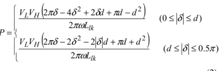
In multi-level modes, the output power is:
( )
( )
⎪ ⎪
⎩
⎪ ⎪
⎨
⎧
≤ + ≤
+
−
−
≤
− ≤ + +
−
=
) 5 . 0 2 (
2 2 2
) 0
2 ( 2 4 2
2 2
2 2
π πω δ
π δ δ πδ
πω δ π δ δ
πδ
L d
d d d V
V
L d
d d d V
V P
lk H
L
lk H
L
(2) When d = π in (2), the three-level operation mode shifts into two-level mode, and (2) is same with (1) as well.
When δ = 0 , the power can be controlled by:
( d )
L d V P V
lk H
L ⋅ −
= 2 πω π (3) From (3), it is clear that the delivered power can be controlled by duty cycle without phase-shift and that extend to another operation mode. However, this mode is out of range for this paper and will not be described here.
B. Circulating Current
Calculation on the waveforms in Figs. 3, yields the rms value of i T 1 a , or I
T1a:
( ) ( ( ) ( ) )
π
δ δ
π δ π
δ π
3
)
( 32 13 12 2
1 2 3
1 I2 dI d I I dI II dI
ITa − + − + − + + − − +
=
(3)
where
( )
( )
( )
⎪ ⎪
⎪ ⎪
⎩
⎪⎪ ⎪
⎪
⎨
⎧
+ +
= −
=
− +
−
= +
=
=
−
−
= +
=
lk
L a H
T
lk
L a H
T peak
lk L a H
T
L
V d t V
i I
L
V d V t d
i I I
L V d t V
i I
ω π
π δ
ω π
δ π
ω π
δ π
2 ) 2 ) ( (
2
) 3 ( 2
) 2 (
2 ) 4
(
4 1 3
3 1 2
1 1 1
And because of the difference between the turn ratio of T
1and that of T
2, the rms value of i
T2ais:
2 1 2 1
T T
a a T
T N
I I
−
= (4) where N
T1-T2equals to n
2/n
1.
C. ZVS ranges
From Fig. 2 and Fig. 5, the conditions of soft switching in boost mode and Buck mode depend on the magnitude of I
T1a, I
T1a+I
T1band I
Ldcat t
1, t
3, t
5and t
7, respectively. So we can get the similar equations with those described in [10].
(Boost mode)
⎪ ⎪
⎩
⎪ ⎪
⎨
⎧
>
+
<
>
+
>
).
( ) ( ) (
; 0 ) (
);
( ) ( ) (
; 0 ) (
7 7
2 7 1
5 1
3 3
2 3 1
1 1
t I t I t I
t I
t I t I t I
t I
Ldc a
T a T
a T
Ldc a
T a T
a T
(5)
(Buck mode)
⎪ ⎪
⎩
⎪ ⎪
⎨
⎧
<
+
>
>
+
<
. 0 ) ( ) (
; 0 ) (
; 0 ) ( ) (
; 0 ) (
7 2 7 1
5 1
3 2 3 1
1 1
t I t I
t I
t I t I
t I
a T a
T a T
a T a
T a T
(6)
From the section II, the soft switching conditions in multi- level mode are shown in (7) and (8).
(Boost mode)
⎪ ⎪
⎩
⎪ ⎪
⎨
⎧
<
>
>
− +
>
<
<
+ +
. 0 ) ( , 0 ) (
; 0 )
( ) (
; 0 ) ( , 0 ) (
; 0 )
( ) (
7 1 4
2
4 2 4 1
2 1 0
2
0 2 0 1
t i t i
I t i t i
t i t i
I t i t i
a T a
T
Ldc a
T a T
a T a
T
Ldc a
T a T
(7)
(Buck mode)
⎪ ⎪
⎩
⎪ ⎪
⎨
⎧
>
+
>
>
<
+
<
<
0 ) ( ) (
0 ) ( , 0 ) (
0 ) ( ) (
0 ) ( , 0 ) (
8 2 8 1
5 2 5
1
3 2 3 1
0 2 0
1
t i t i
t i t i
t i t i
t i t i
a T a T
a T a
T
a T a T
a T a
T
(8)
D. Input current ripple
The input current ripple is limited by the inductor, L
dc. The ripple current ΔI
Ldcof input current I
Ldccan be calculated as:
dc FC dc
Ldc FC L
V L
t I V
ω
= π Δ
= ⋅
Δ (9)
where Δt is the on-time of switch S
2during each switching cycle and L
dcis the input inductance.
IV. E XPERIMENTAL V ERIFICATIONS
In order to verify the operation principle of the proposed converter analyzed above, a prototype was built in lab. For the transformer turn ratio and leakage inductance design, it is necessary to satisfy the following criteria: 1) at heaviest load condition, to keep the DC bus voltage constant, φ is limited under the maximum phase shift angle; 2) Trade-off between the turns ratio and auxiliary inductance is to lower RMS current and extend ZVS operation range.
TABLE I. S
PECIFICATIONS, P
ARAMETERS ANDC
OMPONENTSInput voltage 30-60 VDC
Output voltage 400 VDC
Output power 1 kW
Switches S
1~S
4IRFP4568PBF (150 V/154 A) Switches Q
1, Q
2IRFP450LC (500V/14A) Transformer core Ferrite N87, EI 64 Transformer turns, T1
T2 4:16=n
14:8=n
2Input inductor L
dc80 uH
Auxiliary inductor 60 uH
Switching frequency 40 kHz
Digital controller TMS320F2808
Figure7: Waveforms in Boost mode with two-level. CH1: v
T1b+v
T2b(500 V/div);
CH2: v
CO(200 V/div); CH3: i
T1a(blue 10 A/div); CH4: i
Ldc(green 10 A/div).
Figure 8: ZVS waveforms of the primary side switch in Boost mode with two voltage levels. CH1: v
GSS2(20V/div); CH2: v
DSS2(100 V/div); CH3: i
T1a(blue 10 A/div); CH4: i
T1b(green 10 A/div).
Figure 9: ZVS waveforms of the secondary side switch in Boost mode with two voltage levels.CH1: v
GSS5(20V/div); CH2: v
DSS5(200 V/div); CH3: i
s(10 A/div).
Figure 10: Waveforms in Boost mode with three voltage levels. CH1: v
T1b+v
T2b(500 V/div); CH2: v
CO(200 V/div); CH3: i
T1a(blue 10 A/div); CH4: i
Ldc(green 10 A/div).
Figure 11: ZVS waveforms of the primary side switch in Boost mode with three voltage levels. CH1: v
GSS2(20V/div); CH2: v
DSS2(100 V/div); CH3: i
T1a(blue 10 A/div); CH4: i
T1b(green 10 A/div).
Figure 12: ZVS waveforms of the primary side switch in Boost mode with three voltage levels. CH1: v
GSS4(20V/div); CH2: v
DSS4(100 V/div); CH3: i
T1a(blue 10 A/div); CH4: i
T1b(green 10 A/div)
Figure 13: ZVS waveforms of the primary side switch in Boost mode with three voltage levels. CH1: v
GSS4(20V/div); CH2: v
DSS4(200 V/div); CH3: i
s(10 A/div).
To achieve high output power and low profile of the converter, two planar EI transformers were designed for the converter. In order to minimize the leakage inductance, a sandwiched winding structure was employed and the windings are arranged as: 2-turn (primary):8-turn (secondary):8-turn (secondary):2-turn (primary) for T1 and 2-turn (primary): 8- turn (secondary):2-turn (primary) for T2. The transformers were tested by HP impedance analyzer, and the measured leakage inductances are 109 nH and 103 nH for T1 and T2, respectively, at 40 kHz. The leakage inductance is too small to be as the energy interface element in this converter, as shown in (1) and (2), so one extra inductor of 60 uH was used at the secondary side of transformer for testing. The specifications of the converter are given in Table I.
The Figs. 7-13 show the experimental Boost mode waveforms at 550 W, respectively. Fig. 7 and Fig. 10 show the waveforms of the primary voltage v
T1b+v
T2b, secondary voltage v
CO, primary side current i
T1aand input current i
Ldcunder two- level mode at V
FC=30 V, and three-level mode at V
FC= 40 V, respectively. The experimental waveforms are in agreement with Fig. 2 and Fig. 3.
Fig. 8 and Fig. 9 show the gate drive signal, voltage cross the drain and source of S
2and S
5, the primary side current i
T1aand i
T2a, and the secondary side current i
s, respectively, at V
FC=30 V, under two-level mode. Fig. 11, Fig. 12 and Fig. 13 show the ZVS conditions of S
2, S
4and S
5, at V
FC=40 V under three-level mode. All the switches shown in the figures realize ZVS on, and the experimental results are in agreement with the theoretical analysis well.
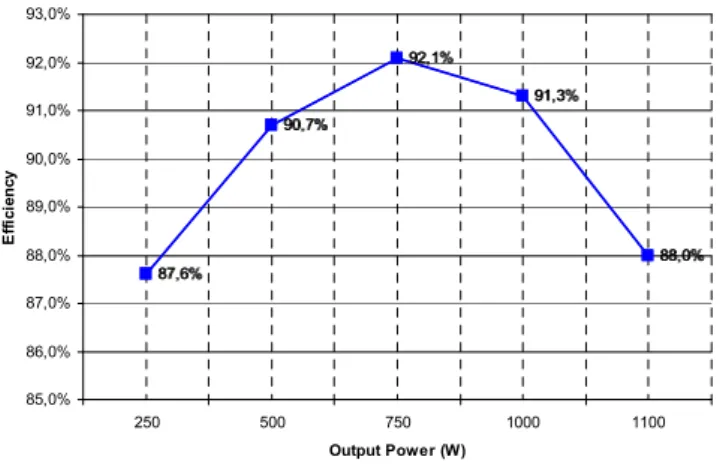
The efficiency in two-level mode at V
FC=30 V and V
O=400
V is measured and efficiency curve illustrating the efficiency in
different output power conditions is plotted in Fig. 14. At light
load condition, the efficiency is lower, due to the primary side
switches working under hard switching. Because the output
87,6%
90,7%
92,1%
91,3%
88,0%
87,6%
90,7%
92,1%
91,3%
88,0%
85,0%
86,0%
87,0%
88,0%
89,0%
90,0%
91,0%
92,0%
250 500 750 1000 1100
Output Power (W)
Efficiency