different interlayers for preparing Si-based nanoporous
alumina template
M.T. Wu, I.C. Leu,a)and M.H. Hon
Department of Materials Science and Engineering, National Cheng Kung University, 701 Tainan, Taiwan
(Received 14 July 2003; accepted 5 December 2003)
The fabrication and applications of porous anodic alumina (PAA) have been studied for decades. Recently, preparation of PAA template directly formed on Si has been developed to enhance the performance of the fabricated nanostructures. However, less attention is paid to the anodization mechanism of the Al film on the Si substrate. In the current study, the PAA template was fabricated on Si of which an interlayer was sandwiched between the Al film and the Si substrate. The anodization behavior of the Al film, especially at the alumina–substrate interface, was investigated through the observation of the variation of oxidation current and the structural change of alumina. Different degree of dissolution at the pore base of alumina was revealed when a different interlayer was introduced, leading to the formation of the arched pore bottom. At the same time, difference in the variation of current was also observed as the pore base reached the alumina–Si interface. These features were different from those observed in conventional anodization of Al foils. The findings in this study are of scientific and technological importance for the template-mediated growth of nanostructures, especially for those to be integrated into Si devices.
I. INTRODUCTION
In recent years, more attention has been paid to the fabrication of nanoscaled structures due to their unique properties for applications in many fields.1–3
For this purpose, many processes have been developed to produce nanostructures and nanodevices, such as electron-beam lithography, focused ion-beam etching, and scanning-probe-based nanolithography processes. However, these methods are relatively time-consuming and expensive and are not considered practical for large-area patterning. Therefore, other processes potentially desirable to reduce the cost and the duration of the fabrication were inten-sively studied. One way to circumvent these obstacles is to use the naturally occurring materials as the templates for the fabrication of nanostructures.
Porous anodic alumina (PAA) is composed of close-packed hexagonal cells, each with a nanopore in the cen-ter.4 The pore characteristics of PAA can be controlled by varying the anodization conditions, including electro-lyte type, electroelectro-lyte concentration, applied voltage, or temperature.5Moreover, PAA with highly ordered pore arrays could be obtained after a sufficient period of anodization if the condition of choice was appropriate.6 And most important, the process for the fabrication of PAA of large area is relatively facile and economical. Therefore, many researches have been focused on the
fabrication of nanostructures by using PAA as a mask or a template. For example, Almawlawi et al., who used PAA as a mask, have transferred a two-dimensional pore array to the substrates by ion milling.7
In the meanwhile, a large number of materials, such as carbon, metals (Ni, Fe, Co, and so forth), and semiconductors (CdS, ZnO, and so forth)8–10
have also been deposited into PAA to produce one-dimensional nanostructures applied to the field emission, magnetic, optical, and sensing devices. Nevertheless, one problem encountered in these pro-cesses is the poor adhesion between the deposit and the substrate. Conventionally, after depositing a conducting layer on the backside, the PAA obtained by anodizing an Al foil was usually directly placed on the substrate with-out other pretreatments, implying that some parts of the PAA may not closely attach to the substrate. In other words, parts of the deposit in the template may also not closely adhere to the substrate. This would lead to the separation of the deposit from the substrate after remov-ing the template. Therefore, a template closely attached to the substrate is needed to improve the adhesion be-tween the deposit and the substrate. One approach to fabricate such a template is to directly anodize an Al thin film deposited on substrate material.
Recently, several studies have been reported to de-scribe the applications of the PAA template obtained by directly anodizing an Al film deposited on the strate, including the pattern transfer to the silicon sub-strate and fabrication of micropillars and Ni nanowires
a)
Address all correspondence to this author. e-mail: [email protected]
on the silicon (or ITO) substrates.11–15 However, less attention has been paid to the growth behaviors of the PAA produced from the Al film,16,17 especially to the PAA/Si systems. To the best of our knowledge, only just a little information for the fabrication of PAA on Si has been revealed.11,14,15
Some anodization behaviors at the alumina–Si interface and alumina–interlayer (Ti, Pt, and SiO2 layer)–Si interface have been reported.
11,14,15 However, the correlation between the variation of current and the structural changes of alumina for the preparation of Si-based nanoporous template has not been clearly described, especially for those obtained during a prolonged anodization step (after the Al film is completely consumed). As far as nanodevice integration is concerned, it is important to reveal the characteristics of the anodization of the Al film on the Si substrate, because Si is the most important material in the ultra large scale integration (ULSI) processes. Moreover, the growth characteristics of alumina at the metal–substrate interface must also be emphasized due to its importance for the subsequent pat-tern transfer and fabrication of nanostructures on Si sub-strates. A better control of the experimental procedure would be beneficial to improve the adhesion between the template (and/or deposit) and the substrate. In some cases, a template with pores of high aspect ratio was desired, that is, a thicker Al film must be deposited on the substrate before anodization. A higher degree of intrinsic stress will be induced with the increase of the film thick-ness, leading to the poor adhesion between the Al film and the Si substrate if an appropriate adhesive layer is not introduced.15
For a multilayered Al film, some disconti-nuities formed between Al layers will be helpful to the release of stress, like the stress relaxation through the formation of dislocations in bulk materials. For this pur-pose, in the current study, one-step anodization was con-ducted on the multilayered Al film on the Si substrate. Besides, Ti and SiO2layers were introduced respectively between the Al films and the Si substrates to study the growth characteristics of alumina at the interface. Some results different from those of the conventional anodiza-tion of Al foils were revealed. First, the structural changes were observed at the pore base, which was dis-similar to the semispherical pore bottom for the oxide obtained on an Al foil. Second, unlike the monotonic decrease of the current in the conventional anodization process, a fluctuation in current was found for the anodi-zation of the multilayered Al film. These variations would be correlated in the current study through the ob-servation of changes in the oxidation current and the morphologies of the oxide.
II. EXPERIMENTAL
Before deposition of Al film, some n-type silicon wa-fers (Silicon Inc., (100), 1–10⍀-cm, Cartina, NY) were
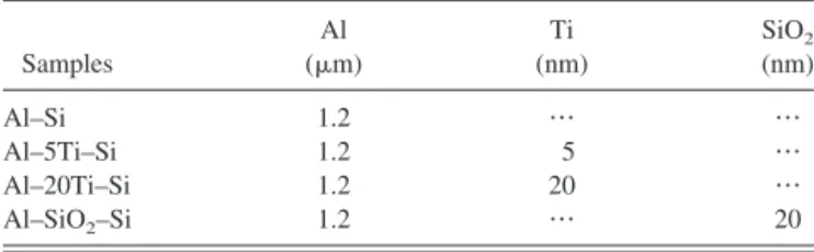
covered with a thin SiO2and a Ti layer, respectively. The SiO2layer of 20-nm thickness was prepared by thermal oxidation using high-temperature tube furnace, whereas the Ti layer of either 5- or 20-nm thickness was deposited by E-beam evaporation. Generally, the SiO2 layer was introduced as a barrier against the oxidation of Si when the Al film was consumed completely during anodization whereas the Ti layer served as an adhesive layer that prevents the separation of the Al film from the Si sub-strate. After the deposition of SiO2 or Ti layers, the Al film was then deposited on the substrate using the E-beam evaporation for three cycles. The thickness of Al film obtained in each cycle was 400 nm, so that the total thickness of this multilayered Al film was 1.2 m. An electric contact was placed to the backside of the Si substrate, which was protected by wax. The codes of different specimens are denoted in Table I.
Because a thin oxide layer would form on the surface of the Al film readily upon its exposure to air, the Al film was immersed into a mixture of 6 wt% H3PO4and 1.8 wt% H2Cr2O4 at 40 °C for 10 min to remove the native oxide layer before anodization. The anodization was conducted in 0.3 M oxalic acid solution in a cooling circulation bath at 13 °C. The fluctuation of the bath temperature was ±0.1 °C. To minimize the effect of the diffusion limitation of species and the heat transfer, the solution was vigorously stirred to improved the unifor-mity of the temperature distribution. During anodization, the variation of the oxidation current was recorded by a data acquisition equipment (Agilent, 34970A, Elgin, IL). To investigate the intrinsic characteristics of the oxide, the anodized specimens were treated without any pore-enlarging process. Finally, the morphology of the oxide was observed by a scanning electron microscope (Philips XL-40EFG, Eindhoven, Netherlands).
III. RESULTS AND DISCUSSION
Figure 1 shows the dependence of the current density on the anodization time for specimens with different in-terlayers anodized at 40 V. The curve 1 in Fig. 1(a) shows the current transient for the Al foil under conven-tional anodization condition. The current reached a steady state within a few minutes, indicating that the growth of the oxide was continuous and stable during the whole process. The curve 2 in Fig. 1(a) shows the TABLE I. Parameters of interlayers and multilayered Al films.
Samples Al (m) Ti (nm) SiO2 (nm) Al–Si 1.2 ⭈⭈⭈ ⭈⭈⭈ Al–5Ti–Si 1.2 5 ⭈⭈⭈ Al–20Ti–Si 1.2 20 ⭈⭈⭈ Al–SiO2–Si 1.2 ⭈⭈⭈ 20
variation of the oxidation current for the Al–Si substrate. Two main features different from those of the curve 1 could be observed. First, during the oxidation of the mul-tilayered Al film (stage I), a fluctuation of current could be found. Leaving the temporary fluctuation region aside, the curve could still be drawn as a continuous line, showing that a stable growth of the oxide would still proceed within each Al layer. Similar features are also found in Figs. 1(b) and 1(c). It is reasonable to argue that there may be some compositional discontinuities at the interface between any two Al layers due to a temporary exposure to the ambient during the deposition of Al. During the oxidation, the continuous growth of the oxide would be interrupted as the pore base extended to the interface, implying that some variations of the current should be observed. Besides, the current fluctuated for two times during the whole anodization process, coin-ciding with the number of the interfaces (two interfaces within three Al layers). Therefore, it is believed that the fluctuation of the current during the anodization of the multilayered Al film was caused by the variation of the electrochemical behavior at the interface between any two Al layers, which will be further discussed later. The lower oxidation current of Al film compared with that of the Al foil was attributed to the relatively higher resis-tance of the Si substrate. For the Al–SiO2–Si substrate, the average oxidation current of the Al film was even lower than that of the Al–Si and Al–20Ti–Si (designated for film structures with Ti interlayer of 20 nm) substrates because a thin insulating SiO2layer was sandwiched be-tween the multilayered Al film and the Si substrate. Sec-ond, after a rapid decrease, the oxidation current recov-ered and finally reached a low value (stage II). Such a feature could be observed for both the anodization of Al–Si and Al–20Ti–Si substrates [Figs. 1(a) and 1(b)]. For the Al–20Ti–Si substrate, the current still decreased monotonically for a period of time before it increased again, different from that for the Al–Si substrate. The inset in Fig. 1(b) shows the dependence of current on the anodization time of Al–5Ti–Si (designated for film struc-tures with Ti interlayer of 5 nm) and Al–20Ti–Si sub-strates in stage II. A period of 20 min was needed before the current increased again for the Al–20Ti–Si substrate whereas only 10 min were necessary for the Al–5Ti–Si substrate. It indicates that the monotonic decrease in cur-rent was related to the thickness of the Ti layer, more precisely, the duration of the anodic oxidation of the Ti layer. The recovery of current has also been observed for the anodization of Al film on the glass substrate and on the Si substrate covered with a thin gold layer, but without a monotonic decrease of current before the re-covery.16–18 For the Al–SiO2–Si substrate, the current almost went to zero after the rapid falling, as shown in Fig. 1(c). Though some features in the stage I (except the fluctuation of the current) have been reported,14
the FIG. 1. Dependence of current on the anodization time for the
differ-ent combination of interlayers of (a) Al–Si, (b) Al–Ti–Si, and (c) Al–SiO2–Si.
current variation in the prolonged anodization has not been fully revealed for the preparation of the Si-based nanoporous alumina template. These variations in current should be closely related to the structural changes of the oxide and the electrochemical reactions at the oxide– metal and the oxide–Si interfaces, as will be discussed in detail in the following.
To facilitate the observation of the transition of the anodic film at different time in the whole oxidation pro-cess, the anodization of different substrates was also con-ducted under a higher voltage (60 V). The variation of the current obtained at 60 V was similar to that obtained at 40 V, except a higher average value of the current. Figure 2 shows the structural changes of the oxide for different anodization time at 60 V on the Al–Si substrate. The inset in each picture shows a high magnification
image at the pore bottom for each condition. Generally, anodic films are formed at the oxide–metal interface in-volving the migration of Al3+ and O2−/OH−, according the following reactions19–21
: Al= Al3++ 3e− , (1) 2Al3++ 3H2O= Al2O3+ 6H + , (2) 2Al+ 3O2−= Al2O3+ 6e − . (3)
Most of the anodic current is attributed to reaction (1), and the growth of oxide and the generation of hydrogen ions are related to reactions (2) and (3). Reactions (1) to (3) dominated the anodization behavior of the multilay-ered Al film in stage I, as well as that of the Al foil. Because the Al layer was exposed to air before the next
FIG. 2. SEM images of structural changes at the interface on the Al–Si substrate. The images of (a), (b), (c), (d), and (e) correspond to the points of a, b, c, d, and e in the current curve, respectively.
deposition, a native oxide would be formed on the sur-face of each Al layer22for the multilayered Al films used in this study. Hence, there was a thin oxide sandwiched between any two Al layers. As the pore base reached the interface of Al layers, the growth of the channel would be delayed temporarily due to the relatively high resistance of the native oxide. This process would lead to the decrease of current. As the pore base ran through the native oxide, a new balance of the pore diameter was established and the current increase again, like the phenomenon of “overshooting” of current for the con-ventional anodization of Al foils.21Some defects might be formed in this period; however, they would be re-paired through the subsequent oxidation of the underly-ing Al film. Figures 2(a) and 2(b) show the cross-sectional morphologies of the oxide corresponding to points a and b in the current curve, respectively. The pore base remained hemispherical even though the oxidation had ever been interrupted at points a and b. As the pore base reached the Si substrate, the continuous Al film transformed into the Al pyramids between the pores [Fig. 2(c)]. Therefore, the effective area of the Al film decreased, leading to the dramatic falling of the oxidation current. The Al pyramids would vanish when the oxida-tion proceeded to point d; in the meanwhile, a void was formed beneath each pore, as shown in Fig. 2(d). In a previously reported study, the formation of the voids at the alumina–Si interface is attributed to the stress created by volume expansion as the Al pyramids are anodized, causing the pore bottom to be squeezed inward.15
This indicates that the distance between the pore bottom and the alumina–Si interface should increase after the Al pyramids are completely consumed. However, according to the results in the current study, two important features at the alumina–Si interface should be noticed. First, the distance between the pore bottom and the alumina–Si interface did not increase in the whole anodization proc-ess. For example, as the pore base reached the alumina– interface, the distance between the pore bottom and the interface was about 60 nm, as shown in Fig. 2(c). The distance did not exceed 60 nm in the prolonged anodi-zation process, as shown in Figs. 2(d) and 2(e). Second, the thickness of the barrier layer decreased from 60 nm to 40 nm. Therefore, it is suggested that the formation of the void beneath the pore is predominantly caused by the excessive dissolution occurred at the alumina–Si inter-face. This might be caused by the hydrogen ion-assisted dissolution for which the generation of the hydrogen ions is attributed to the oxidation of the underlying Si substrate23
Si+ 2H2O= SiO2+ 4H++ 4e− . (4) After passing point d, the current immediately recov-ered for a while, and finally went to zero. The recovery of the current is also a feature of the current variation for
the formation of SiO2-barrier-type-oxide under potentio-static conditions.24 It is worthy to note that when the oxidation proceeded to point e, the pore base became arched. Some oblique pores beside the pore wall could be observed, which would be formed during the oxidation of the Al pyramids. The formation of the voids and arched pore bases indicated that the excessive dissolution also occurred at the oxide–Si interface in the time interval between regions d and e. Nevertheless, the stress induced by the anodization of Al pyramids may play a role in the formation of voids.
Figures 3(a) and 3(b) show the scanning electron microscopy (SEM) images of the multilayered Al film before and after anodization, respectively. The insets show higher magnification images near the interfacial regions of the multilayered Al film [in Fig. 3(a)] and of the porous alumina [in Fig. 3(b)], respectively. No obvi-ous interface was observed between the Al layers, indi-cating that almost no defects formed during the deposi-tion of the Al film. Therefore, the fluctuadeposi-tion in current during the anodization of the Al film should be caused by the compositional discontinuities (formation of the native oxide) between Al layers, as mentioned previously. Because the thickness of the native oxide is commonly reported to be very thin (about 2 nm),22a new balance in the pore characteristics will soon be established as the pore bottom runs through the interface. Straight channels across the whole template without obvious defects could be obtained, indicating that the self-organization process
FIG. 3. SEM images of (a) the multilayered Al film before anodiza-tion and (b) an alumina template after anodizaanodiza-tion.
of pores would not be disturbed for the anodization of a multilayered Al film, as shown in Fig. 3(b).
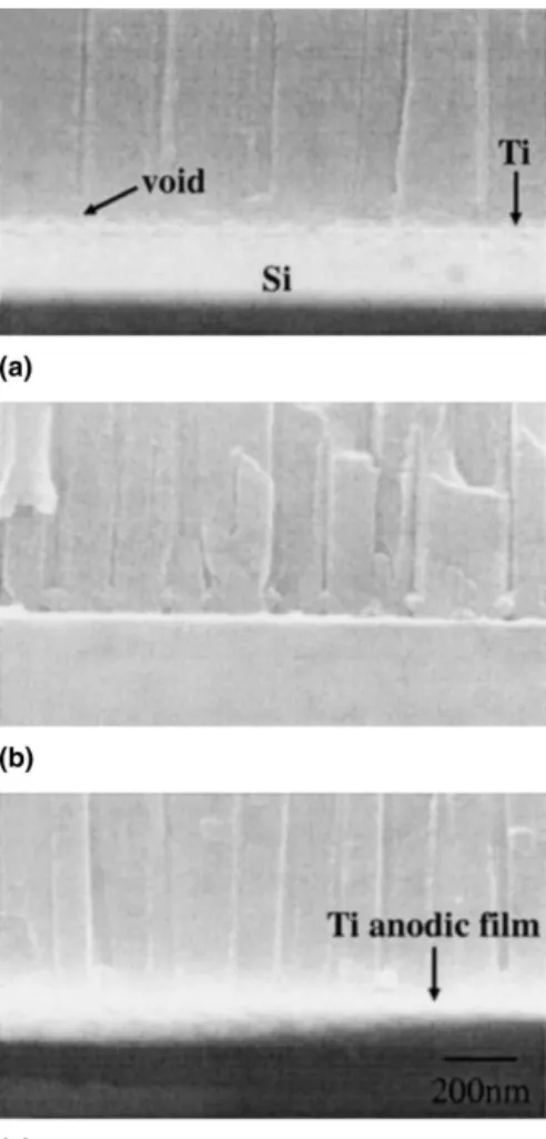
Though a Ti layer has been used as an adhesion layer, only the morphologies of the pore bottom after the pore opening were revealed for the anodization of an Al film on the Ti-coated Si substrate.15
It is very important to realize the structural changes at the alumina–Si interface on the Al–Ti–Si substrate because an isolated pore is desired after the barrier layer is removed. Figure 4 shows the SEM images of the structural changes at the alumina– Si interface on the Al–20Ti–Si substrate anodized at 60 V. After the complete consumption of the Al pyra-mids, some tiny voids directly beneath the pores were observed, and some pore bases also became somewhat arched, as shown in Fig. 4(a). Such structural variation indicates that the excessive dissolution at the pore base also occurs at the alumina–Ti interface. Under such a high voltage, the anodic oxidation of the sandwiched Ti interlayer was possible. Some hydrogen ions would be generated during the anodization of Ti,25–27 leading to the acidification at the pore base of alumina and the enhancement of the dissolution at the alumina–Ti inter-face. Following the rapid falling, a plateau of current
could be observed [shown in Fig. 1(b)], relating to the stable oxidation of the Ti interlayer. During this period, all the pore bases became arched, as shown in Fig 4(b). The recovery of current occurred after the Ti layer was completely oxidized, similar to that observed on the Al–Si substrate. At the same time, the arched pore bases became looser than those obtained on the Al–Si substrate for the same anodization duration, implying the higher degree of excessive dissolution at the alumina–Si inter-face on the Al–20Ti–Si substrate, as shown in Fig. 4(c). Figure 5 shows the SEM images of the alumina–Si interface on the Al–SiO2–Si substrate anodized at 60 V. The pore base remained as an integral part without the formation of the void after the Al pyramids were com-pletely oxidized, different from those observed on the Al–Si and Al–20Ti–Si substrates. Some oblique pores were still formed beside the pore base due to the anodi-zation of the Al pyramids. Only few voids directly under some pores could be found after the prolonged anodiza-tion, indicating a lesser degree of excessive dissolution than that on Al–Si and Al–20Ti–Si substrates. No obvi-ous recovery of current was observed during the whole anodization of Al film on the Al–SiO2–Si substrate [Fig. 1(c)] because a 20-nm-thick SiO2layer existed and the anodization rate of the underlying Si was then re-duced. The formation of voids might be mainly caused by the hydrogen ion-assisted dissolution, of which the generation of the hydrogen ions was attributed to reac-tion (4). The occurrence of anodic oxidareac-tion of Si was reasonable for the Al–SiO2–Si substrate under such a high voltage (60 V) because the electrolyte would penetrate the cracks of the sandwiched SiO2interlayer; no matter the cracks were stress-induced or dielectric
FIG. 4. SEM images for the alumina–substrate interface on the Al– 20Ti–Si substrate.
FIG. 5. SEM images for the alumina–substrate interface on the Al–SiO2–Si substrate.
breakdown-induced.28 The results obtained on the Al– SiO2–Si substrate could be considered as some more evi-dence that the formation of voids on the Al–Si and Al–20Ti–Si substrates is predominantly caused by the hydrogen ion-assisted dissolution.
According to what mentioned above, a schematic diagram of the structural changes at the alumina–Si interface was presented for the Al–Si and Al–20Ti–Si substrates in Fig. 6. As extending to the alumina– substrate interface, the pore base maintains hemispheric and the Al pyramids are formed between the pore bot-toms, as shown in Fig. 6(a). Such characteristics could be
observed for all types of the substrates in the current study, indicating that this feature is dominated by the anodization behavior of the Al film. When the pore bases reach the Si substrate (or the Ti interlayer), the Al pyra-mids keep on being converted into alumina with the progress of the oxidation process. Assuming that the di-rection of the current is perpendicular to the metal sur-face,29
additional dissolution will occur beside the pore bottom, leading to the gradual formation of rectangular pore base, as shown in Fig. 6(b). At the same time, when the pore base reaches the Si substrate (or the Ti inter-layer), other anodic processes such as oxidation of the Si or Ti are likely to occur under such a high voltage. The anodic oxidation of Si or Ti will accompany the genera-tion of the hydrogen ions, leading to the acidificagenera-tion of the electrolyte and an excessive dissolution of oxide at the pore base. Therefore, voids directly beneath the pores are formed. When the Al pyramids are completely oxi-dized, some oblique pores will be formed beside the pore wall. The formation of the oblique pore has also been described for the anodization of the Al film on ITO glass.16 Finally, an arched pore base is formed through the combined action of the oblique pores and the en-larged void due to excessive dissolution under the pore bottom, as shown in Fig. 6(c). For the Al–SiO2–Si sub-strate, no void was formed beneath the pore when the Al pyramids were completely oxidized. After a prolonged anodization, few arched pore bases could be observed, but most of the pore bottoms remained as an integral part. This might be caused by the slow oxidation of the un-derlying Si because an insulating SiO2 layer was pre-sandwiched between the Al film and the Si substrate.
IV. CONCLUSIONS
In this study, the relationship between the oxidation behavior and the current variation for the anodization of Al film on the Si substrates was presented, especially the structural changes at the alumina–substrate interface. Different from the conventional anodization of the Al foil, fluctuation of the current was observed for the oxi-dation of the multilayered Al film. It is believed that the fluctuation in current was caused by the discontinuities between the Al layers. When the Al film was completely consumed, an immediate recovery of current occurred on the Al–Si substrate. Such a feature could also be ob-served on the Al–20Ti–Si substrate after the complete oxidation of the Ti interlayer. The recovery of the current was caused by formation of SiO2 barrier-layer-type-oxide through the anodization of the underlying Si substrate.
Moreover, some structural changes at the pore base were found when the Al film was completely oxidized. First, voids directly beneath the pores were formed, in-dicating that an excessive dissolution should occur at the alumina–substrate interface. The additional dissolution FIG. 6. Schematic diagram of the structural changes at the alumina–Si
interface for the Al–Si and Al–20Ti–Si substrates. The arrows show the direction of the current flow at the pore bottom during anodization. Theoretically, the current flow should be perpendicular to the surface of the pore bottom.
would be caused by the hydrogen ion-assisted dissolu-tion, for which the generation of the hydrogen ions was attributed to the oxidation of the Si substrate or the Ti interlayer. This only occurred on the Al–Si and Al–20Ti– Si substrates because the oxidation could easily proceed at the alumina–substrate interface under such a high volt-age. Second, through the oxidation of the Al pyramids, some oblique pores beside the pore wall were also formed. Therefore, the arched pore bases were finally formed at the alumina–substrate interface when the an-odization was finished. The issues discussed in the cur-rent study are important for the template-mediated proc-esses. One can understand the features of the alumina template by monitoring the current variation during the anodization, which is beneficial to the subsequent fabri-cation of the nanostructures on the Si substrate.
ACKNOWLEDGMENT
The authors acknowledge financial support from the National Science Council of Taiwan, Republic of China, under Contract No. NSC 91-2216-E-006-028.
REFERENCES
1. S. Khizroev, J.A. Bain, and D. Litvinov, Nanotechnology 13, 619 (2002).
2. O.K. Varghese, D. Gong, M. Paulose, K.G. Ong, C.A. Grimes, and E.C. Dickey, J. Mater. Res. 17, 1162 (2002).
3. G. Rosenman, P. Urenski, A. Agronin, Y. Rosenwaks, and M. Molotskii, Appl. Phys. Lett. 82, 103 (2003).
4. F. Keller, M.S. Hunter, and D.L. Robinson, J. Electrochem. Soc.
100,411 (1953).
5. J.P. O’Sullivan and G.C. Wood, Proc. R. Soc. (London) A 317, 511 (1970).
6. A.P. Li, F. Müller, A. Birner, K. Nielsch, and U. Gösele, J. Appl. Phys. 84, 6023 (1998).
7. D. Almawlawi, K.A. Bosnick, A. Osika, and M. Moskovits, Adv. Mater. 12, 1252 (2000).
8. P.M. Paulus, F. Luis, M. Kröll, G. Schmid, and L.J. Jongh, J. Magn. Magn. Mater. 224, 180 (2001).
9. Y. Yang, H. Chen, Y. Mei, J. Chen, X. Wu, and X. Bao, Acta Materia. 50, 5085 (2002).
10. Y.C. Wang, I.C. Leu, and M.H. Hon, J. Mater. Chem. 12, 2439 (2002).
11. D. Crouse, Y.H. Lo, A.E. Miller, and M. Crouse, Appl. Phys. Lett.
76,49 (2000).
12. A.I. Vorobyova, V.A. Sokol, and E.A. Outkina, Appl. Phys. A 67, 487 (1998).
13. S.Z. Chu, K. Wada, S. Inoue, S. Todoroki, Y.K. Takahashi, and K. Hono, Chem. Mater. 14, 4595 (2002).
14. M.S. Sander and L-S. Tan, Adv. Funct. Mater. 13, 393 (2003). 15. O. Rabin, P.R. Herz, Y-M. Lin, A.I. Akinwande, S.B. Cronin, and
M.S. Dresselhaus, Adv. Funct. Mater. 13, 631 (2003).
16. S.Z. Chu, K. Wada, S. Inoue, and S. Todoroki, J. Electrochem. Soc. 149, B321 (2002).
17. A. Mozalev, A. Poznyak, I. Mozaleva, and A.W. Hassel, Electro-chem. Comm. 3, 299 (2001).
18. Y. Yang, H. Chen, Y. Mei, J. Chen, X. Wu, and X. Bao, Solid State Commun. 123, 279 (2002).
19. G.E. Thompson, Y. Xu, P. Skeldon, K. Shimizu, S.H. Han, and G.C. Wood, Philos. Mag. A 55, 651 (1987).
20. G. Patermarakis and K. Moussoutzanis, Electrochim. Acta 40, 699 (1995).
21. F. Li, L. Zhang, and R.M. Metzger, Chem. Mater. 10, 2470 (1998).
22. K. Shimizu, K. Kobayashi, P. Skeldon, G.E. Thompson, and G.C. Wood, Corros. Sci. 3, 701 (1997).
23. X.G. Zhang, Electrochemistry of Silicon and Its Oxide (Kluwer Academic/Plenum Publishers, New York, 2001), p. 48. 24. V. Lehmann, Electrochemistry of Silicon (Wiley-VCH Verlag
GmbH, Morlenbach, Germany, 2002), p. 79.
25. D.J. Blackwood, L.M. Peter, and D.E. Williams, Electrochim. Acta 33, 1143 (1988).
26. G.P. De Pauli, M.C. Giordano, and J.O. Zerbino, Electrochim. Acta 28, 1781 (1983).
27. M. Pourbaix, Atlas of Electrochemical Equilibria in Aqueous
So-lutions (NACE, Houston, 1974).
28. V. Lehmann, J. Electrochem. Soc. 143, 1313 (1996).
29. V.P. Parkhutik and V.I. Shershulsky, Phys. D: Appl. Phys. 25, 1258 (1992).